Note: Descriptions are shown in the official language in which they were submitted.
CA 02234878 1998-04-1
DESCRIPTION
METHOD AND DEVICE FOR CONTROLLING TRACKING OF OPTICAL MEMORY CARD
TECHNICAL FIELD
The present invention relates to a method and device for
controlling the tracking of an optical memory card. In particular
it relates to a method and device for controlling the tracking
of an optical memory card, which is capable of not only spPP~; ng
up the operations of recording and reproducing in an optlcal
memory card, but also capable of ensuring prevention of
overwriting and similar operational errors resulting from
mistakes in track holding.
BACKGROUND ART
Generally speaking, optical memory cards are plastic cards
of a stipulated size configured in such a ~nne~ that their
recording area may be recorded on to and reproduced with the aid
of a laser beam.
Fig. 10 shows the recording area 102 of a conventional
optical memory card 101. As may be seen from the enlarged
drawing, the recording area 102 has data recording tracks 1 and
guide tracks 2 arranged alternately on it. The data recording
tracks 1 are the parts which serve to record data, while the
guide tracks 2 are formed at a specified interval, which is
required for the purpose of tracking control whereby the
irradiation position of the laser beam used for recording and
reproducing is stabilized.
CA 02234878 1998-04-1~
Here, the reflection factors of the data recording tracks
1 and the guide tracks 2 differ, and a comparison between the two
shows that of the data recording tracks 1 is high, while that of
the guide tracks 2 is low.
The recording pits 3 are sections with low reflection
factors which are formed by a laser beam within the recording
tracks 1 at the time of recording. The presence or absence of
these recording pits 3 corresponds to the digital codes 0 and 1.
Fig. 11 is a diagram illustrating the configuration of the
optical system which records and reproduces in~ormation for the
optical memory card 101.
In Fig. 11, a laser beam emitted from a laser diode 103 is
rendered into a parallel beam by a collimator lens 104, is
incident upon a diffraction grating 105, and is split into
~nnll~~~able light rays.
The light rays which have been split with the aid of the
diffraction grating 105 are directed on to a beam splitter 106,
the zero-order beam being used as the main beam for recording and
reproducing data, while the +-order beam is used as a sub-beam
for tracking control.
Part of the rays which are incident upon the beam splitter
106 are reflected in a 90~ direction and directed on to a power
monitor 114 which monitors the strength of the light source. The
r~m~n~ng rays pass through the beam splitter 106 and proceed
straight ahead by way of a reflecting mirror 107 and ob~ective
lens 108 to converge as three spots on the recording area 102 of
the optical memory card 101.
Reflected off the recording area 102, the rays are rendered
- CA 02234878 1998-04-1~
into a parallel beam once more by the ob~ective lens 108, pass
through the reflecting mirror 107, and are reflected in a 90~
direction by the beam splitter 106. They then proceed by way of
a collimator lens 109 and concave lens 110 to assume a long focal
length and be directed on to an edge mirror 111.
This edge mirror 111 is a reflecting mirror which is located
so as to screen half the rays, so that they are divided into half
the main beam along with the +-order light of the sub-beam on the
one hand, and the r~m~;n;ng half of the main beam along with the
--order light of the sub-beam on the other.
Having been divided by means of the edge mirror 111, the
half of the main beam and the +-order light of the sub-beam
proceed straight ahead to form an image on an photosensor 112,
while the ro -;n;ng half of the main beam and the --order light
of the sub-beam are reflected in a 90~ direction to form an image
on an photosensor 113.
The rays which form images on the photosensors 112 and 113
are here converted into electric signals.
It should be noted that the main beam (0-order light) 7 and the
sub-beams (+-order light) 8a, 8b, having passed through the
objective lens 108, are directed on to the recording area 102 as
illustrated in Fig. 10. The recording pits 3 are formed by this
main beam 7 in the center of the data recording track, which is
to say equidistantly from the two adjoining guide tracks 2.
For this reason, the main beam 7 must always be directed on to
the center of the data recording track 1. Consequently, tracking
control is implemented with the aid of the sub-beam 8 (or the
sub-beams 8a and 8b) and the guide tracks 2.
CA 02234878 1998-04-1~
The main beam 7 and the sub-beams 8a and 8b are always
incident on the recording area 102 at a prescribed interval. When
the main beam 7 is incident in the correct position, half of each
of the sub-beams 8a and 8b is incident upon the data recording
track 1, and the rem~in~er upon the guide track 2.
Inasmuch as the edge mirror 111 causes the reflected light
of the two sub-beams 8a and 8b to form images on separate
photosensors (eg the sub-beam 8a on the photosensor 112, and the
sub-beam 8b on the photosensor 113), it is possible to calculate
the reflection factor of the positions upon which the respective
sub-beams are incident.
If each of the beams 8a and 8b are incident in the correct
position, the reflection factors of the positions in which they
are incident are e~ual, as therefore are the respective strengths
of the reflected light.
However, if the irradiation position of a beam is displaced
to the left or to the right, the difference between the
respective strengths of the reflected light of the sub-beams 8a
and 8b appears as a positive or negative value. This difference
is converted into an electric signal and fed back as a tracking
error signal. This drives the ob~ective lens 108 in a horizontal
direction, controlling it so that it assumes a state where this
tracking error signal is 0, namely where the main beam 7 is
incident in the correct position.
Fig. 12 illustrates the logical data configuration of the
recording area 102. In the recording area 102 are recorded, apart
from a sector 120 which is the part where data is recorded, a
lead-in 121 which allows the device for recording and reproducing
~' CA 02234878 1998-04-1~
the optical memory card (not shown in the drawing) to achieve bit
synchronization during recording and reproduction, a SYNC mark
122 which facilitates ~rame synchronization, a sOS 123 which is
necessary in order to detect the position at which the sector 120
begins, and other information.
In the lead-in 121, not only is the SYNC mark 122 recorded,
but the recording pit 3 is formed for each recording interval
(synonymous with the digital code 1 1 1 1 . . . ).
The device for recording and reproducing the optical memory
card (not shown in the drawing) has a device for generating a
synchronizing signal (not shown in the drawing). The memory card
101 is scAnn~ at a scanning rate such that the synchronizing
signal output from the device for generating a synchronizing
signal matches the initialization signal of each bit which is
detected by sCAnn~ng the lead-in 121, and bit synchronization is
achieved by maint~; n; ng this s~Annl ng rate.
A modulation system wherein a synchronizing signal is
included in the recorded data is sometimes employed in order to
ensure that the achieved bit synchronization is maintained, and
the synchronizing signal is extracted from the signal detected
during reproduction.
Here, the SYNC mark 122 is formed by arranging recording
pits 3 in a pattern which is not generated by modulation, and
this is used so that the device for recording and reproducing the
optical memory card (not shown in the drawing) can acquire the
frame signal.
The frames are sequences of bits when the signal processing
circuit within the device for recording and reproducing the
CA 02234878 1998-04-1~
optical memory card (not shown in the drawing) is processing
signals. The device for recording and reproducing the optical
memory card (not shown in the drawing) has a counter tnot shown
in the drawing) for achieving frame synchronization. When it has
counted up to the number of bits which constitute a frame, it
outputs a frame synchronizing signal and clears the counter
value.
Here, the SYNC mark 122 is recorded at the beginning (or
end) of the frame. The device for recording and reproducing the
optical memory card (not shown in the drawing) scans the optical
memory card 101. When it detects the SYNC mark 122, it clears the
counter (not shown in the drawing) for achieving frame
synchronization, ensuring that frame synchronization is achieved.
When a track holding mistake occurs in the conventional
method for controlling the tracking of an optical memory card as
described above, and vibration of the actuator or an external
shock of some kind causes the main beam while scanning a data
recording track 1 to migrate to a different data recording track
1, control is implemented in such a r-nne~ that the main beam
tracks the center of the recording track 1 to which it has
migrated.
In such a case, a problem occurs in that if the track to
which the main beam has migrated is a data recording track 1 on
which data has already been recorded, the data is overwritten and
lost.
In order to prevent the overwriting of data, it is vital to
distinguish between a data recording track 1 which has already
been recorded and one which has not. It has been suggested that
CA 02234878 1998-04-1~
a modulation system might be adopted whereby recording pits 3 are
formed within a specified interval even if the data recorded is
a succession of O signals (not forming recording pits), but
efficiency is poor. Moreover, even if this system is adopted, it
is difficult to prevent overwriting altogether because it occurs
before there is time to detect that the track to which the main
beam has migrated is a data recording track 1 on which data has
already been recorded.
Meanwhile, conventional devices for recording and
reproducing optical memory cards have a circuit for generating
a synchronizing signal in order to achieve bit synchronization.
They also have an actuator and control circuit whereby it is
possible to maintain a constant sc~nning rate in order to ensure
that the bit synchronization achieved by sc~nn;ng the lead-in 121
is maint~in~. This means that if the action of recording and
reproduction is to be speeded up, it is necessary to improve the
accuracy of the sc~nn~ng rate, including the accuracy of the
actuator.
Moreover, not only are the lead-in 121 and SYNC mark 122,
which are vital so that the device for recording and reproducing
the optical memory card to achieve bit and frame synchronization,
recorded on the conventional optical memory card, but a
modulation system is adopted whereby a synchronizing signal is
included in the data which is recorded for the purpose of
ensuring that bit synchronization is maintained. Thus, the
adoption of a modulation system such as allows data recording
tracks 1 which have already been recorded to be distinguished
from those which have not results in problems of lower recording
CA 02234878 1998-04-1~
efficiency and a reduction in the amount of data which can be
recorded on one optical memory card.
SUMMARY OF THE INVENTION
It is an object of the present invention to provide a method
and device for controlling the tracking of an optical memory card
which not only make it possible to ensure that overwriting and
similar problems arising from track holding mistakes are avoided,
but also serve to speed up the actions of recording and
reproduction.
With a view to the att~inm~nt of the abovementioned object,
the present invention provides a method for controlling tracking
o~ an optical memory card having in a recording area alternately
data recording tracks for recording data, and guide tracks for
guiding a position of a laser beam used for recording and
reproduction, the tracking of the optical memory card being
implemented on the basis of a detection output of photosensors
located in correspo~en~-~- with the guide tracks, characterized
int that the method comprises the steps of: forming on the guide
tracks patterns comprised of a combination of at least two types
of guide track segment of a prescribed length synchronized with
a recording interval in relation to the data recording tracks;
and extracting a synchronizing signal for recording and
reproduction in relation to the data recording tracks by r~1 ng
the patterns with the aid of the photosensors.
It may be configured in such a ~-nner that the patterns
comprised of the combination of guide track segments of the
prescribed length differ in correspondence with each of the data
CA 02234878 1998-04-1~
recording tracks, and a track holding error in the data recording
tracks is detected on the basis of a read output of the patterns
with the aid of the photosensors.
It may also configured in such a manner that the patterns
comprised of the combination of guide track segments of the
prescribed length differ in correspondence with each of the data
recording tracks, and identification of the data recording tracks
is carried out on the basis of a read output of the patterns with
the aid of the photosensors.
Here, the guide track segments of the prescribed length may
comprise first guide track segments which are slightly shorter
than n times the recording interval, and second guide segments
which are slightly shorter than 2n times the recording interval.
Moreover, the tracking of the optical memory card may be
implemented on the basis of a low-frequency component of the
photosensor, and extraction of the synchronizing signal and
identification of the tracks of the optical memory card are
carried out on the basis of a high-frequency component of the
photosensor.
Here, the patterns formed on the guide tracks may comprise
patterns which are repeated in a cycle below that of the number
of bits for which errors can be corrected in relation to the data
recording tracks, identification of the data recording tracks is
carried out on the basis of combinations of patterns formed on
two guide tracks between which the data recording track is
interposed.
Also, the invention provides a device for controlling the
tracking of an optical memory card having in a recording area
' CA 02234878 1998-04-1~
alternately data recording tracks for recording data, and guide
tracks for guiding a position of a laser beam used for recording
and reproduction, wherein patterns are formed on the guide
tracks, said patterns being comprised of a combination of at
least two types of guide track segment of a prescribed length
synchronized with a recording interval in relation to the data
recording tracks, and the tracking of the optical memory card is
implemented on the basis of detection outputs of a first
photosensor and a second photosensor located in correspondence
with two guide tracks between which the data recording track is
interposed, characterized in that the device comprises:
a first low-band pass filter which serves to extract a low-
band frequency component from a detection output of the first
photosensor;
a first high-band pass filter which serves to extract a
high-band frequency component from the detection output of the
first photosensor;
a second low-band pass filter which serves to extract a
low-band frequency component from a detection output of the
second photosensor;
a second high-band pass filter which serves to extract a
high-band frequency component from the detection output of the
second photosensor;
tracking control means for carrying out the tracking of the
optical memory card on the basis of a difference between the
detection output of the first low-band pass filter and that of
the second low-band pass filter;
an AND-circuit for extracting a synchronizing signal for
' CA 02234878 1998-04-1~
recording and reproduction in relation to the data recording
track on the basis of a logical product of the detection output
of the first high-band pass filter and that of the second high-
band pass filter;
a first comparative circuit for comparing the detection
output of the first high-band pass filter with a prescribed first
reference pattern;
a second comparative circuit for comparing the detection
output of the second high-band pass filter with a prescribed
second reference pattern; and
identification means for identifying the data recording
track on the basis of comparative outputs of the first and second
comparative circuits.
Here, the configùration may be such that the patterns formed
on the guide tracks comprise a combination of first guide track
segments being slightly shorter than n times the recording
interval and second guide track segments being slightly shorter
than 2n times the recording interval, and a combination of the
pattern formed in the two guide tracks between which the data
recording track is interposed differs at least among adjoining
data recording tracks.
Moreover, the configuration may be such that the patterns
formed on the guide tracks comprise patterns which are repeated
in a cycle below that of the number of bits for which errors can
be corrected in relation to the data recording tracks.
Also, the invention is characterized by having in a
recording area alternately data recording tracks for recording
data and guide tracks for guiding a po~ition of a la~er beam
11
CA 02234878 1998-04-1~
used for recording and reproduction, and having on the guide
tracks patterns comprised of a combination of at least two types
of guide track segment of a prescribed length synchronized with
a recording interval in relation to the data recording tracks.
Here, the configuration may be such that the patterns formed
on the guide tracks comprise a combination of first guide track
segments being slightly shorter than n times the recording
interval and second guide track segments being slightly shorter
than 2n times the recording interval.
Moreover, the configuration may be such that the combination
of patterns formed on the two guide tracks between which the data
recording track is interposed differs at least among adjoining
data recording tracks.
Furthermore, the configuration may be such that the patterns
formed on the guide tracks comprise patterns which are repeated
in a cycle below that of the number of bits for which errors can
be corrected in relation to the data recording tracks.
BRIEF DESCRIPTION OF THE DRAWINGS
Fig. 1 is a diagram which serves to illustrate an embodiment
of the track configuration of an optical memory card used in a
method and device for controlling the tracking of an optical
memory card to which the present invention pertains;
Fig. 2 is a schematic drawing depicting an embodiment of a
circuit whereby a tracking error signal, track holding signal
and bit synchronizing signal are extracted if the track
configuration illustrated in Fig. 1 is adopted;
Fig. 3 is a schematic drawing depicting another embodiment
12
-
'' CA 02234878 1998-04-1~
of the circuit whereby the tracking error signal, track holding
signal and bit synchronizing signal are extracted if the track
configuration illustrated in Fig. 1 is adopted;
Fig. 4 is a timing chart of a part that extracts the
synchronizing signal and track holding signal of the circuit
illustrated in Fig. 3 which corresponds to a part of the track
configuration shown in Fig. l;
Fig. 5 is a timing chart of a part that extracts the
synchronizing signal and track holding signal of the circuit
illustrated in Fig. 3 which corresponds to another part of the
track configura~ion shown in Fig. 1;
Fig. 6 is a drawing which illustrates the method of signal
processing within a computing unit in the circuit configuration
depicted in Fig. 3;
Fig. 7 is a diagram which serves to illustrate another
embodiment of the track configuration of an optical memory card
used in the method and device for controlling the tracking of an
optical memory card to which the present invention pertains;
Fig. 8 is a diagram which serves to illustrate another
embodiment of the track configuration of an optical memory card
used in the method for controlling the tracking of an optical
memory card and device for that purpose to which the present
invention pertains;
Fig. 9 is a diagram which serves to illustrate another
embodiment of the track configuration of an optical memory card
used in the method and device for controlling the tracking of an
optical memory card to which the present invention pertains;
Fig. 10 is a diagram illustrating a track configuration in
13
'' CA 02234878 1998-04-1~
the recording area of a conventional optical memory card;
Fig. 11 is a diagram illustrating the configuration of an
optical system which records and reproduces information for an
optical memory card; and
Fig. 12 is a diagram which illustrates a logical
configuration of the conventional memory card.
BEST MODE FOR CARRYING OUT THE INVENTION
There follows an embodiment whereby the optical memory card
and device for that purpose to which the present invention
pertains will be described in greater detail with the aid of the
attached drawings.
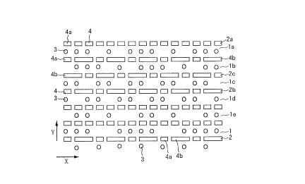
Fig. l is a diagram which serves to illustrate an embodiment
of the track configuration of an optical memory card used in the
method for controlling the tracking of an optical memory card and
device for that purpose to which the present invention pertains.
The track configuration of the optical memory card
illustrated in Fig. l is such that data recording tracks 1, which
form recording pits 3, and guide tracks 2 are arranged
alternately. The guide tracks 2 are not continuous as in the
conventional device illustrated in Fig. 10, but are made up of
rows each comprising a plurality of guide track segments 4.
Two types of guide track segment 4 are used, viz. a guide
track segment 4a which is slightly shorter than the recording
interval of the data recording track 1, and a guide track segment
4b which is slightly shorter than twice the recording interval
of the data recording track 1. Repeated patterns formed by virtue
of the arrangement of these guide track segments 4 consist of
14
CA 02234878 1998-04-1~
cycles of three recording interval lengths wherein three bits of
data are recorded.
It will therefore be clear from the method of detecting
track holding mistake~ described below that provided the error
correction capacity of the recording and reproduction device for
the optical memory card is not less than three bits, it will be
possible to correct track holding mistakes without any
interruption to the process of sCAnn i ng the recording area of
the optical memory card.
There are three possible permutations of cycle of three
recording interval lengths, namely guide track 2a, guide track
2b and guide track 2c, which with an interposed data recording
track 1 yield nine combinations.
However, as will be evident from the method of detecting
track holding mistakes which is described below, a data recording
track 1 with guide tracks 2b on either side or with guide tracks
2c on either side does not allow a synchronizing signal to be
extracted, so that it is impossible to use these configurations.
It will also be evident that where a data recording track
is bordered on one side by a guide track 2a (eg as at the top of
the drawing) and on the opposite side (center of the drawing) by
a guide track 2b or 2c, the method of detecting track holding
mistakes described below detects both as the same pattern, with
the result that only one of them can be used.
This means that the maximum number of permutations of data
recording track 1 interposed between guide tracks 2 which can be
used is represented by the five data recording tracks la-le
illustrated in Fig. 1.
CA 02234878 1998-04-1~
Guide tracks 2 composed of guide track segments 4 in this
Tnz~nn~.~ are irradiated with sub-beam a~ depicted in Fig. lO, and
the reflected beams detected with the aid of photosensors 112 and
113, thus allowing a tracking error signal, track holding signal
and synchronizing signal to be extracted from the detection
output.
Fig. 2 is a schematic drawing depicting an embodiment of the
circuit whereby the tracking error signal, track holding signal
and synchronizing signal are extracted.
In Fig. 2, an photosensor 11 corresponds to the photosensor
112 illustrated in Fig. 10, while an photosensor 12 corresponds
to the photosensor 113 illustrated in that drawing.
The output of the photosensor 11 is input to a low-band pass
filter 13 and a high-band pass filter 15, allowing respectively
the low-band frequency component and high-band frequency
component of the photosensor 11 to be extracted.
Similarly, the output of the photosensor 12 is input to a
low-band pass filter 14 and a high-band pass filter 16, allowing
respectively the low-band frequency component and high-band
frequency component of the photosensor 12 to be extracted.
The low-band frequency component of the output of the
photosensor 11 extracted in the low-band pass filter 13 and the
low-band frequency component of the output of the photosensor 12
extracted in the low-band pass filter 14 are input to a computing
unit 19.
The computing unit 19 deducts the low-band fre~uency
component of the output of the photosensor 12 extracted in the
low-band pass filter 14 from the low-band frequency component of
16
CA 02234878 1998-04-1~
the output of the photosensor 11 extracted in the low-band pass
filter 13, and outputs the result as a tracking error signal.
In other words, the fact that during scanning of the
recording area of the optical memory card the optical head moves
at high speed in the X direction means that by extracting the
low-band frequency component of the output of the photosensor 11
in the low-band pass filter 13, and the low-band frequency
component of the output of the photosensor 12 in the low-band
pass filter 14, it is possible to extract signals independently
of breaks between the guide track segments 4 of the guide tracks
2. This enables tracking control by means of a tracking error
signal as in the conventional method.
Meanwhile, the high-band frequency component of the output
of the photosensor 11 extracted in the high-band pass filter 15
and the high-band frequency component of the output of the
photosensor 12 extracted in the high-band pass filter 16 each
become signals wherein breaks between the guide track segments
4 of the guide tracks 2 have been detected.
The high-band frequency component of the output of the
photosensor 11 extracted in the high-band pass filter 15 and the
high-band frequency component of the output of the photosensor
12 extracted in the high-band pass filter 16 are shaped into
square-wave signals in a waveform shaper 17 and waveform shaper
18 respectively before being input to an AND-gate 20.
Here, the arrangement of the guide track segments 4 of the
guide tracks 2 is configured in such a m~n~er that for each
recording interval length of the data recording track 1 there is
a break in at least one of the guide tracks 2 between which the
CA 02234878 1998-04-1~
data recording track 1 is interposed. Thus, it is possible to
extract an initializing bit synchronizing signal from the AND-
gate 20 for each such recording interval. Inasmuch as these bit
synchronizing signals are independent of the scanning rate, it
is possible to achieve correct bit synchronization during
recording and reproduction in relation to the recording area of
the optical memory card without improving the accuracy of the
sc~nn~ng rate.
The output of the waveform shapers 17 and 18 is input to
serial-parallel converters 21 and 22.
The serial-parallel converters 21 and 22 convert the signals
input from the waveform shapers 17 and 18 to parallel data with
the aid of the synchronizing signals output from the AND-gate 20,
and input them to comparators 25 and 26.
Meanwhile, for instance, a first standard pattern
corresponding to the upper of the two guide tracks between which
the scanned data recording track 1 is interposed is set in a
st~n~rd pattern generator 23. The st~n~rd pattern generator 23
generates this first st~n~rd pattern as parallel data, and
inputs it to the comparator 25.
Similarly, for instance, a second st~n~rd pattern
corresps~lng to the lower of the two guide tracks between which
the s~nn~ data recording track 1 is interposed is set in a
standard pattern generator 24. The standard pattern generator 24
generates this second st~n~rd pattern as parallel data, and
inputs it to the comparator 26.
The comparator 25 compares the parallel data which has been
converted in the serial-parallel converter 21 and the first
18
CA 02234878 1998-04-1~
standard pattern which has been generated by the standard pattern
generator 23. If they match, it outputs a high-level signal. The
output of the comparator 25 is input to an AND-gate 27.
Meanwhile, the comparator 26 compares the parallel data
which has been converted in the serial-parallel converter 22 and
the second st~n~rd pattern which has been generated by the
st~n~d pattern generator 24. If they match, it outputs a high-
level signal. The output of the comparator 26 is input to the
AND-gate 27.
The AND-gate 27 takes the logical product of the input
signals and outputs it as a track holding signal.
In other words, if the input signals are both high-level,
which is to say if the two guide tracks between which the scanned
data recording track 1 is interposed match the first and second
standard patterns respectively, a high-level track holding signal
is output from the AND-gate 27 as indicating that the data
recording track 1 is being sc~nne~ correctly.
If a track holding mistake occurs, a low-level signal is
output from the AND-gate 27. If the track configuration of the
card is like the one illustrated in Fig. 1, the arrangement of
the guide track segments 4 is such that one cycle is equal to
three recording interval lengths, and the pattern formed by the
arrangement of the guide track segments 4 of the guide tracks 2
between which the data recording track 1 is interposed is
repeated with five data recording tracks 1 as one cycle. This
means that if the track holding mistake is within the range of
five tracks, it can be detected during the time it takes to scan
three recording intervals.
19
CA 02234878 1998-04-1~
Fig. 3 is schematic drawing depicting another embodiment of
the circuit whereby the tracking error signal, track holding
signal and bit synchronizing signal are extracted.
The circuit illustrated in Fig. 3 is configured in such a
manner as to output a track holding signal which shows not only
whether or not the data recording track 1 is being scanned
correctly, but also how many tracks the beam has slipped if it
has migrated from the correct data recording track 1. In the
configuration illustrated in Fig. 3, the tracking error signal
and the synchronizing signal are extracted in the same m~nn~ as
in Fig. 2.
The configuration illustrated in Fig. 3 differs from that
of Fig. 2 in that it detects in addition which of five data
recording tracks 1 is being sC~nne~ and outputs on the basis of
the relationship between the parallelly sc~nn~ data recording
tracks 1 and the correct data recording track 1 a track holding
signal which shows how many tracks the beam has slipped if it has
migrated from the correct data recording track 1.
In Fig. 3, the output of the serial-parallel converter (S/P)
21, wherein the synchronizing signal output from the AND-gate 20
is used to convert the output of the waveform shaper 17 to
parallel data, is input to comparators (CMP) 250, 251, 252, 253
and 254.
Similarly, the output of the serial-parallel converter (S/P)
22, wherein the synchronizing signal output from the AND-gate 20
is used to convert the output of the waveform shaper 18 to
parallel data, is input to comparators (CMP) 260, 261, 262, 263
and 264.
' CA 02234878 1998-04-1~
Meanwhile, a digital code 000 representing a first pattern
which corresponds to the guide track 2a of the guide tracks 2
illustrated in Fig. 1 is set in a standard pattern generator
(000) 230, and the digital code 000 generated by this standard
pattern generator 230 is input to the comparators 250, 254, 263
and 264.
Similarly, a digital code 010 representing a second
pattern which corresponds to the guide track 2b of the guide
tracks 2 illustrated in Fig. 1 is set in a st~n~d pattern
generator (010) 231, and the digital code 010 generated by this
stAn~d pattern generator 231 is input to the comparators 251,
253, 260 and 262.
In the same ~nner, a digital code lO0 representing a
third pattern which corresponds to the guide track 2c of the
guide tracks 2 illustrated in Fig. 1 is set in a standard pattern
generator (100) 232, and the digital code 100 generated by this
st~ ~d pattern generator 232 is input to the comparators 252
and 261.
As has been explained above, there are five combinations of
pattern of the guide tracks 2 between which the data recording
track 1 is interposed, each with interposition of data recording
tracks from la to le as illustrated in Fig. 1. In the circuit
illustrated in Fig. 3, the comparators 250 and 260 together
detect the combination of patterns corresponding to the data
recording track la, while the comparators 251 and 261 together
detect the combination of patterns correspon~1ng to the data
recording track lb, the comparators 252 and 262 together detect
the combination of patterns corresponding to the data recording
CA 02234878 1998-04-1~
track lc, the comparators 253 and 263 together detect the
combination of patterns corresponding to the data recording track
ld, and the comparators 254 and 264 together detect the
combination of pattern~ corresponding to the data recording track
le.
The pattern signals output from the serial-parallel
converters 21 and 22, and corresponding to the pattern of the
guide track 2a illustrated in Fig. 1 are always 000 . If the
signal generated by the standard pattern generator 230
corresponding to the guide track 2a is 000 , and as a result the
pattern detected by the comparators 250, 254, 263 and 264 is that
of the guide track 2a, a high-level signal is always output.
Meanwhile, the pattern signals output from the
serial-parallel converters 21 and 22, and corresponding to the
pattern of the guide track 2b illustrated in Fig. 1 changes in
the order 010 , 100 , 001 in synchronization with the
synchronizing signal. If the signal generated by the st~n~A~d
pattern generator 231 corresponding to the guide track 2b is
010 , and as a result the pattern detected by the comparators
251, 253, 260 and 262 is that of the guide track 2b, a high-
level signal showing that the result of the comparison is the
same is output for only one of three cycles of the synchronizing
signal. Similarly, if the signal generated by the standard
pattern generator 232 corresponding to the guide track 2c is
100 , and as a result the pattern detected by the comparators
252 and 261 is that of the guide track 2c, a high-level signal
showing that the result of the comparison is the same is output
for only one of three cycles of the synchronizing signal.
22
; CA 02234878 1998-04-1~
In the same ~nne~, the pattern signals output from the
serial-parallel converters 21 and 22, and corresponding to the
pattern of the guide track 2c illustrated in Fig. 1 changes in
the order 100 , 001 , 010 in synchronization with the
synchronizing signal. If the signal generated by the standard
pattern generator 232 corresponding to the guide track 2c is
100 , and as a result the pattern detected by the comparators
252 and 261 is that of the guide track 2c, a high-level signal
showing that the result of the comparison is the same is output
for only one of three cycles of the synchronizing signal.
Similarly, if the signal generated by the st~n~d pattern
generator 231 corresponding to the guide track 2b is 010 , and
as a result the pattern detected by the comparators 251, 253, 260
and 262 is that of the guide track 2c, a high-level signal
showing that the result of the comparison is the same is output
for only one of three cycles of the synchronizing signal.
Consequently, if the photosensor 11 detects the pattern of
the guide track 2a, a high-level signal is output from the
comparators 250 and 254. If the photosensor 11 detects the
pattern of the guide track 2b, a high-level signal is output from
the comparators 251 and 253 for only one of three cycles of the
synchronizing signal, while a similar signal to that output from
the comparators 251 and 253 but with its phase staggered by one
cycle of the synchronizing signal is output from the comparator
252. If the photosensor 11 detects the pattern of the guide track
2c, a high-level signal is output from the comparator 252 for
only one of three cycles of the synchronizing signal, while a
similar signal to that output from the comparator 252 but with
CA 02234878 1998-04-1~
its phase staggered by one cycle of the synchronizing signal is
output from the comparators 251 and 253.
In the same manner, if the photosensor 12 detects the
pattern of the guide track 2a, a high-level signal is output from
the comparators 263 and 264. If the photosensor 12 detects the
pattern of the guide track 2b, a high-level signal is output from
the comparators 260 and 262 for only one of three cycles of the
synchronizing signal, while a similar signal to that output from
the comparators 260 and 262 but with its phase staggered by one
cycle of the synchronizing signal is output from the comparator
261. If the photosensor 12 detects the pattern of the guide track
2c, a high-level signal is output from the comparator 261 for
only one of three cycles of the synchronizing signal, while a
similar signal to that output from the comparator 261 but with
its phase staggered by one cycle of the synchronizing signal is
output from the comparators 260 and 262.
Thus, when the data recording track la is scanned, a high-
level signal is output for only one of three cycles of the
synchronizing signal from an AND-gate 270, which outputs the
logical product of the output of the comparator 250 and that of
the comparator 260. Meanwhile, so long as the data recording
track la is being scanned, a high-level signal is always output
from an OR-gate 300, which outputs the logical sum of the output
signal from the AND-gate 270, a signal wherein this output signal
from the AND-gate 270 is delayed by one cycle of the
synchronizing signal by virtue of a D flip-flop 280, and a signal
wherein the output signal from the D flip-flop 280 is delayed by
one cycle of the synchronizing signal by virtue of a D flip-
24
CA 02234878 1998-04-1
flop 290.
Moreover, when the data recording track lb is scanned, a
high-level signal is output for only one of three cycles of the
synchronizing signal from an AND-gate 271, which outputs the
logical product of the output of the comparator 251 and that of
the comparator 261. Meanwhile, so long as the data recording
track lb is being s~nne~, a high-level signal is always output
from an OR-gate 301, which outputs the logical sum of the output
signal from the AND-gate 271, a signal wherein this output signal
from the AND-gate 271 is delayed by one cycle of the
synchronizing signal by virtue of a D flip-flop 281, and a signal
wherein the output signal from the D flip-flop 281 is delayed by
one cycle of the synchronizing signal by virtue of a D flip-
flop 291. However, the output of the comparator 252 and that of
the comparator 262 are signals of a differing phase, and
therefore so long as the data recording track lb is being
scanned, the output of an AND-gate 272, which outputs the logical
sum of the two, is a low-level signal.
Similarly, when the data recording track lc is scanned, a
high-level signal is output for only one of three cycles of the
synchronizing signal from the AND-gate 272, which outputs the
logical product of the output of the comparator 252 and that of
the comparator 262. Meanwhile, so long as the data recording
track lc is being s~.~nn~, a high-level slgnal is always output
from an OR-gate 302, which outputs the logical sum of the output
signal from the AND-gate 272, a signal wherein this output signal
from the AND-gate 272 is delayed by one cycle of the
synchronizing signal by virtue of a D flip-flop 282, and a signal
CA 02234878 1998-04-1~
wherein the output signal from the D flip-flop 282 is delayed by
one cycIe of the synchronizing signal by virtue of a D flip-
~lop 292. However, the output of the comparator 251 and that of
the comparat~r 261 are signals of a differing phase, and
therefore so long as the data recording track lc is being
sCAnne~, the output of the AND-gate 271, which output~ the
logical sum of the two, is a low-level signal.
In the same ~nn~, when the data recording track ld is
scanned, a high-level signal is output for only one of three
cycles of the synchronizing signal from an AND-gate 273, which
outputs the logical product of the output of the comparator 253
and that of the comparator 263. Meanwhile, so long as the data
recording track ld is being scanned, a high-level signal is
always output from an OR-gate 303, which outputs the logical sum
of the output signal from the AND-gate 273, a signal wherein this
output signal from the AND-gate 273 is delayed by one cycle of
the synchronizing signal by virtue of a D flip-flop 283, and a
signal wherein the output signal from the D flip-flop 283 is
delayed by one cycle of the synchronizing signal by virtue of a
D flip-flop 293.
Furthermore, when the data recording track le is scanned,
a high-level signal is output, so long as the data recording
track le is being scanned, from an AND-gate 274 which outputs the
logical product of the output of the comparator 254 and that of
the comparator 264.
Figs. 4 and 5 are t1 ~ng charts illustrating the detection
of the synchronizing signal and guide track patterns.
Fig. 4 is a t~ ~ng chart where the data recording track la
26
CA 02234878 1998-04-1~
is scanned. Fig. 4 (a) shows the patterns of arrangement of the
guide track segments 4 which comprise the guide track 2a, while
Fig. 4 (b) shows the patterns of arrangement of the guide track
segments 4 which comprise the guide track 2b.
Figs. 4 (c) and 4 (d) illustrate pattern signals
corresponding to the guide tracks shown in Figs. 4 (a) and (b)
respectively after shaping in the waveform shapers 17 and 18.
Since the breaks in the guide tracks 2 have a higher
reflection factor than the guide track segments 4, the output of
the photosensors 11 and 12 is greater for the breaks. This is
reversed during shaping in the waveform shapers 17 and 18, and
therefore the pattern signals in Figs. 4 (c) and 4 (d) are
initializing square waveforms corresponding to the guide track
segments 4.
Fig. 4 (e) illustrates the output of the AND-gate 20 into
which the pattern signals illustrated in Figs. 4 (c) and 4 (d)
have been input.
The AND-gate 20 outputs a high-level signal only when both
inputs are high level, and so outputs a square waveform signal,
which becomes a bit synchronizing signal with the recording
interval of the data recording track 1 as its cycle.
Fig. 4 (f) shows the output of the lower bits of the
serial-parallel converter 21, Fig. 4 (g) that of the central
bits, and Fig. 4 (h) that of the upper bits, from which it will
be seen that the detection pattern of the guide track 2a is
always 000 .
Fig. 4 (i) shows the output of the lower bits of the
serial-parallel converter 22, Fig. 4 (~) that of the central
27
CA 02234878 1998-04-1~
bits, and Fig. 4 (k) that of the upper bits, from which it will
be seen that the detection pattern of the guide track 2b changes
from 010 to 100 and 001 with each cycle of the
synchronizing signal.
Fig. 4 (1) is the output of the AND-gate 270. It will be
seen that a high-level signal is output when the output of the
serial-parallel converter 21 is 000 (Figs. 4 (f), 4 (g) and 4
(h) are all low level), and when the output of the
serial-parallel converter 22 is 010 (Fig. 4 (i) is low level,
Fig. 4 (;) high level, and Fig. 4 (k) low level). Fig. 4 (m) is
Fig. 4 (1) delayed by one cycle of the synchronizing signal by
virtue of the D flip-flop 280, while Fig. 4 (n) is Fig. 4 (m)
delayed by one cycle of the synchronizing signal by virtue of the
D flip-flop 290. It will be seen that taking the logical sum of
Figs. 4 (1), 4 (m) and 4 (n) always produces a high-level signal.
Fig. 5 is a t~ 1 ng chart where the data récording track lb
is s~nn~. Fig. 5 (a) shows the patterns of arrangement of the
guide track segments 4 which comprise the guide track 2b, while
Fig. 5 (b) shows the patterns of arrangement of the guide track
segments 4 which comprise the guide track 2c.
Figs. 5 (c) and 5 (d) illustrate pattern signals
corresponding to the guide tracks shown in Figs. 5 (a) and (b)
respectively after shaping in the waveform shapers 17 and 18.
Since the breaks in the guide tracks 2 have a higher
reflection factor than the guide track segments 4, the output of
the photosensors 11 and 12 is greater for the breaks. This is
reversed during shaping in the waveform shapers 17 and 18, and
therefore the pattern signals in Figs. 5 (c) and 5 (d) are
28
CA 02234878 1998-04-1~
initializing square waveforms corresponding to the guide track
segments 4.
Fig. 5 (e) illustrates the output of the AND-gate 20 into
which the pattern signals illustrated in Figs. 5 (c) and 4 (d)
have been input.
The AND-gate 20 outputs a high-level signal only when both
inputs are high level, and so outputs a square waveform signal,
which becomes a bit synchronizing signal with the recording
interval of the data recording track 1 as its cycle.
Fig. 5 (f) shows the output of the lower bits of the
serial-parallel converter 21, Fig. 5 (g) that of the central
bits, and Fig. 5 (h) that of the upper bits, from which it will
be seen that the detection pattern of the guide track 2b changes
from 010 to 100 and 001 with each cycle of the
synchronizing signal.
Fig. 5 (i) shows the output of the lower bits of the
serial-parallel converter 22, Fig. 5 (~) that of the central
bits, and Fig. 5 (k) that of the upper bits, from which it will
be seen that the detection pattern of the guide track 2c changes
from 100 to 001 and 010 with each cycle of the
synchronizing signal, and the waveform is similar to the
detection pattern of the guide track 2b with its phase staggered
by one cycle of the synchronizing signal.
Fig. 5 (l) is the output of the AND-gate 271. It will be
seen that a high-level signal is output when the output of the
serial-parallel converter 21 is 010 (Fig. 5 (f) is low level,
Fig. 5 (g) high level, and Fig. 5 (h) low level), and when the
output of the serial-parallel converter 22 is 100 (Fig. 5 (i)
29
CA 02234878 1998-04-1~
is low level, Fig. 5 (;) low level, and Fig. 5 (k) high level).
Fig. 5 (m) is Fig. 5 (1) delayed by one cycle of the
synchronizing signal by virtue of the D flip-flop 280, while Fig.
5 (n) is Fig. 5 (m) delayed by one cycle o~ the synchronizing
signal by virtue of the D flip-flop 290. It will be seen that
taking the logical sum of Figs. 5 (1), 5 (m) and 5 (n) always
produces a high-level signal.
In other words, when the data recording track 1 is scanned,
a high-level signal is output from one of the OR-gates 300, 301,
302 and 303, or the AND-gate 274 in accordance with the pattern
~ormed by the arrangement of the guide track segments 4 of the
guide tracks 2 between which the data recording track 1 is
interposed, thus making it possible to check the data recording
track which is being sC~nne~
The output of the OR-gates 300, 301, 302 and 303, and the
AND-gate 274 is input to the computing unit 400.
A scan track signal denoting the data recording track 1
which it is desired to scan is input to the computing unit 400,
and a track holding signal showing how many tracks the beam has
migrated from the correct data recording track 1 is output on the
basis of the output of the OR-gates 300, 301, 302 and 303, and
the AND-gate 274, together with the scan track signal.
To be precise, the computing unit 400 may consist of a ROM
in which a table as illustrated in Fig. 6 has been stored.
In the table illustrated in Fig. 6, the horizontal rows A-E
represent the output of the OR-gates 300, 301, 302 and 303, and
the AND-gate 274, while the vertical columns A-E represent the
desired data recording tracks 1 which the scan track signal
t . CA 02234878 1998-04-1~
denotes. O , ~ 1 , +2 and -2 denote the difference
between the data recording track 1 which it is desired to scan
and the data recording track 1 which is actually being scanned.
Assuming, for example, that the data recording track 1 which
it i~ desired to scan is the data recording track la, and this
track is being scanned, the OR-gate 300 which corresponds to the
data recording track la outputs a high-level signal, while the
OR-gates 301, 302 and 303, and the AND-gate 274 which correspond
to the data recording tracks lb-le output a low-level signal. The
computing unit 400 outputs a track holding signal O , which
shows that it is the correct data recording track 1.
Suppose that a track holding mistake occurs in this state,
and the data recording track 1 jumps from the data recording
track la to the data recording track lc. During the time which
it takes for three bits of data to be reproduced (three recording
intervals to be scanned), the output signal of the OR-gate 300
which corresponds to the data recording track la reverses to low
level, while the output signal of the OR-gate 302 which
corresponds to the data recording track lc reverses to high
level. As a result, a track holding signal -2 is output from
the computing unit 400, showing that the beam has migrated two
tracks downwards (in the negative direction on the Y axis in Fig.
1) from the correct data recording track.
In the device for recording and reproducing optical memory
cards (not shown in the drawing), the beam is returned from the
data recording track lc to the correct data recording track la
on the basis of this track holding signal -2 .
Here, provided that the number of bits by which the device
31
CA 02234878 1998-04-1~
for recording and reproducing optical memory cards (not shown in
the drawing) allows errors to be corrected is three or more, it
is possible to correct three bits of error which have occurred
as a result of a track holding mistake, thus allowing the device
for recording and reproducing optical memory cards to continue
sc~nn;ng the data recording track la without interruption.
Assuming again, for example, that the data recording track
1 which it is desired to scan is the data recording track ld, and
this track is being sCAnn~ the OR-gate 303 which corresponds
to the data recording track ld outputs a high-level signal, while
the OR-gates 300, 301 and 302 which correspond to the data
recording tracks la-lc, and the AND-gate 274 which corresponds
to the data recording tracks le output a low-level signal. The
computing unit 400 outputs a track holding signal 0 , which
shows that it is the correct data recording track 1.
Suppose that a track holding mistake occurs in this state,
and the data recording track 1 jumps from the data recording
track ld to the data recording track lb. During the time which
it takes for three bits of data to be reproduced (three recording
intervals to be sc~nn~ ), the output signal of the OR-gate 303
which corresponds to the data recording track ld reverses to low
level, while the output signal of the OR-gate 301 which
corresponds to the data recording track lb reverses to high
level. As a result, a track holding signal +2 is output from
the computing unit 400, showing that the beam has migrated two
tracks upwards (in the positive direction on the Y axis in Fig.
1) from the correct data recording track.
In the device for recording and reproducing optical memory
CA 02234878 1998-04-1~
cards (not shown in the drawing), the beam is returned from the
data recording track lb to the correct data recording track ld
on the basi~ of this track holding signal +2 .
Here, provided that the number of bits by which the device
for recording and reproducing optical memory cards (not shown in
the drawing) allows errors to be corrected is three or more, it
is possible to correct three bits of error which have occurred
as a result of a track holding mistake, thus allowing the device
for recording and reproducing optical memory cards to continue
sc~nn; ng the data recording track ld without interruption.
Figs. 7-9 illustrate other examples of the track
configuration shown in Fig. 1.
In Fig. 7, n = 1, which is to say that it illustrates an
example where the length of the guide tracks 4 is configured in
such a manner that the guide track segments 4a are slightly
shorter than the recording interval of the data recording track
1, while the guide track segments 4b are slightly shorter than
twice the recording interval, the cycle of arrangement of the
guide track segments 4 being the length of four recording
intervals. In this example, the number of usable combinations of
patterns formed by the arrangement of the guide track segments
4 of the guide tracks 2 between which the data recording track
1 is interposed is eleven, and the range within which it is
possible to correct tracking hold mistakes is a m~x;mum of eleven
ad;oining tracks.
In this case, the time required to detect the track holding
mistake is within the time which the device for recording and
reproducing optical memory cards (not shown in the drawing) takes
CA 02234878 1998-04-1~
to scan four recording intervals of the data recording track 1.
Four bits are made to correspond to the serial-parallel
converters 21 and 22 and the comparators 25 and 26, and it
requires four or more bits which are capable of error correction.
In Fig. 8, n = 1, which is to say that it illustrates an
example where the length of the guide tracks 4 is configured in
such a ~nn~r that the guide track segments 4a are slightly
shorter than the recording interval of the data recording track
1, while the guide track segments 4b are slightly shorter than
twice the recording interval, the cycle of arrangement of the
guide track segments 4 being the length of five recording
intervals. In this example, the number of usable combinations of
patterns formed by the arrangement of the guide track segments
4 of the guide tracks 2 between which the data recording track
1 is interposed is seventeen, and the range within which it is
possible to correct tracking hold mistakes is a m;:~X; mum of
seventeen ad;oining tracks.
In this case, the time required to detect the track holding
mistake is within the time which the device for recording and
reproducing optical memory cards (not shown in the drawing) takes
to scan five recording intervals of the data recording track 1.
Five bits are made to correspond to the serial-parallel
converters Zl and 22 and the comparators 25 and 26, and it
requires five or more bits which are capable of error correction.
In Fig. 9, n = 2, which is to say that it illustrates an
example where the length of the guide tracks 4 is configured in
such a ~nn~ that the guide track segments 4c are slightly
shorter than twice the recording interval of the data recording
34
CA 02234878 1998-04-1~
track 1, while the guide track segments 4d are slightly shorter
than ~uadruple the recording interval, the cycle of arrangement
of the guide track segments 4 being the length of six recording
intervals. In this example, the number of usable combinations of
patterns formed by the arrangement of the guide track segments
4 of the guide tracks 2 between which the data recording track
1 is interposed is five, and the range within which it is
possible to correct tracking hold mistakes is a mAx;mum of five
ad~oining tracks.
In this case, the time required to detect the track holding
mistake is within the time which the device for recording and
reproducing optical memory cards (not shown in the drawing) takes
to scan six recording intervals of the data recording track 1.
Since the bit synchronizing signal which is obtained has a cycle
of two bits, it is necessary to have a circuit which converts
this signal into a bit synchronizing signal with a one-bit cycle.
INDUSTRIAL APPLICABILITY
In the present invention, data recording tracks for
recording data, and guide tracks whereof the function is to guide
the position of the laser beam used for recording and
reproduction, are located alternately, and patterns are formed
by the guide tracks, said patterns consisting of a combination
of at least two types of guide track segment of a prescribed
length synchronized with the recording interval in relation to
the data recording tracks. This means that it is possible to
extract a tracking error signal, track holding signal and bit
synchronizing signal from the patterns which are detected by
CA 02234878 1998-04-1~
photosensors corresponding to the guide tracks. The tracking
error sinal is used to control tracking and inhibit track holding
mistakes, and the track holding signal to detect and correct
track holding mistakes, thus preventing overwriting of data
recording tracks which have already been recorded on, and
inhibiting interruption of scanning resulting from track holding
mistakes.
Moreover, inasmuch as the bit synchronizing signal is
independent of the scAnn i ng rate of the device, the device can
easily achieve bit synchronization, allowing the operation of
recording and reproduction to be speeded up without improving the
accuracy of the s~.~nn ~ ng rate.
Furthermore, inasmuch as the tracking error signal, track
holding signal and bit synchronizing signal are independent of
the modulation system, it is possible to adopt an efficient
modulation system, while the fact that it is not necessary to
record data on to the data recording track to achieve
synchronization means that it is possible to contribute to the
realization of a highly efficient optical memory card capable of
high-speed operation.