Note: Descriptions are shown in the official language in which they were submitted.
CA 022349~0 1998-04-16
W O 97/16922 PCTAJS96/17505
IM[AGING SYSTEM
Field of the Invention
This invention relates generally to the field of im~gin~; systems used in
e S fluorescence microscopy and more particularly to an electro-optical im~gin~
device adapted to be used in combination with an optical system such as a
conventional microscope that displays a diffraction-limited, video image which
can be used in tr~n~mi~sion, reflection, and fluorescence microscopy.
Back~round of the Invention
Fluorescence microscopes evolved from ordinary transmitted light
microscopes with the addition of an excitation filter in the illllmin~tion path and an
emission filter in the viewing path. Low contrast and low fluorescence intensitywere problems. For these reasons, transmitted light fluorescence has generally
been abandoned. Significant improvements came from using reflected light
methods to view the fluorescence from the same side as the illllmin~tion. Calledincident light, reflected light, or epi-illllmin~tion~ the fluorescent emission does not
have to pass through the sample to be detected, which attenuates and diffuses the
already weak radiation. The objective lens is also the condenser, elimin~ting
centering and alignment problems. Difficulties remain, however, in using low
power objectives because the low mlmerical ~l Lu.e is an inefficient collector of
the emitte-l fluorescence radiation and it is difficult to obtain a ~ti~f~ctory image.
It is known to apply video technology to the im~ging of microscope
samples. Video cameras, laser scanners, and flying spot scanners have all been
applied to microscopy.
Applying video im~ging techniques to fluorescence microscopy has been
difficult. The weak emission from fluorescent samples is difficult to detect with
ordinary video cameras. Expensive, cooled SIT and CCD cameras have been used
with some success. However, most systems produce only monochromatic images,
and require either high power light sources that can potentially damage delicatesamples, or long exposure times to gain sufficient signal for analysis. Typically,
camera systems cannot run in real time at full resolution. The m~ximum
resolution is limited by the camera image sensor, which is usually less than the diffraction limit of the optics.
CA 022349~0 1998-04-16
W O 97/16922 PCT~US96/1750S
Better video im~ing has been achieved with laser sc~nning confocal
microscopes, which may cost up to $300,000. Laser sc~nning microscopes use a
laser to create a spot of light that scans across the sample in a raster pattern. The
fluorescent emission is detected in the reflection mode by a photomultiplier tube
5 (PMT) whose sensitivity is much higher than video cameras. The deflection of the
laser beam is accomplished by mechanical servo-galvanometers that oscillate x-
and y-axis steering mirrors. The mechanical scan size can be varied to allow
ch~n~in~s the image ~leld of view, thus ch~nginP the m~gnific~tion of the image.Because the ~c~nning is mechanical, the maximum frame rate is limite-l to about
10 4Hz, and a usable image is achieved in 2-10 seconds. The disadvantages of laser
sc~nning microscopes include high expense, slow image scan rate, monochromatic
light source, and others.
This invention relates to the improvement of a tr~n~mitte-l light full color
microscope described in US Patent # 5,430,807.
It is accordingly an object of the present invention to provide an advanced
sc~nnin~ fluorescence im~gin~ system that produces an output for display on a
high resolution video display terminal and provides an electronic digital
representation of the image.
Another object of the present invention is to provide a flurorescence
20 sc~nning im~ing system that operates at the diffraction limit of the optics to
which it is connected and is therefore an im~ging system operating at the
uppermost limits of resolution.
Another object of the present invention is to provide a sc~nning
fluorescence im~ing system that operates at a variety of m~nification powers in
25 both tr~n~mitte~l light and reflected light modes.
Yet Another object of the present invention is to provide a flurorescence
sc~nning im~ing system that provides simultaneous reflected and transmitted
light images.
Still another obJect of the present invention is to provide a SCilnning
30 fluorescence im~ing system that includes the ability to enhance or suppress
portions of the field of view.
A still further object of the present invention is to provide a sc~nning
fluorescence im~ging system that includes an instantaneous m~gnification zoom
feature.
. ,
CA 022349~0 1998-04-16
W O 97/16922 PCT~US96/17505
A still further object of the present invention is to provide a sczlnning
im~ging system that includes full color reflected and transmitted light images in
addition to fluorescent images using a common illnmin~tion source.
A still further object of the present invention is to provide a sc~nnin
fluorescence im~gin~ system that is reliable and inexpensive.
Summarv of the Invention
The benefits and advantages of the present invention are achieved in an
im~ging system characterized by its ability to produce a diffraction limited output
10 signal representative of a sample positioned on a sample plane. The im~in~
system comprises a cathode ray tube, an optical lens system and a means for
sensing. The cathode ray tube comprises a spot scanner means for generating an
min~te-1 spot that scans in a raster pattern. The raster pattern is composed of a
predetermined number of horizontal lines that are spaced vertically from each
15 other a predetermined and equal distance. An illllmin~ted spot scans
correspondingly in the raster pattern and wherein the spot is positioned in an object
plane. The system images in a diffraction limitl~-1 manner the object plane on to
the sample plane, such that the image of the spot is the smallest diffraction limited
size as limite~l by the optical lens system. Filters inserted before the sample allow
only the excitation band of wavelengths to impinge upon the sample, and filters
inserted in the sensor path allow only the fluorescence emission wavelengths to
impinge upon the sensors.
Brief Description of the Drawin~s
Some of the features and advantages of the present invention having been
briefly stated, others will appear from the detailed description which follows, when
taken in connection with the accompanying drawings -
Figure la illustrates schematically a conventional transmitted white light
and fluorescence optical im~gin~ system, such as a compound microscope.
Figure 1 b illustrates schematically a transmitted white light and
fluorescence im~ging system according to the present invention.
Figure 2a illustrates schematically a conventional reflected white light and
fluorescence optical im~ging system, such as a compound microscope.
CA 022349~0 1998-04-16
W O 97/16922 PCTAUS96/17505
Figure 2b illustrates schematically a reflected white light and fluorescence
optical im~ging system according to the present invention.
Figure 3a illustrates schematically a conventional combination tr~n.cmitt~d
and reflected white light and reflected fluorescence im~ging system, such as a
S compound microscope.
Figure 3b illustrates schematically a combination transmitted and reflected
light white light and fluorescence im~ging system according to the present
invenhon.
Figure 4 illustrates schem~tic~lly a cathode ray tube (CRT) according to the
10 present invention.
Figure 5 illustrates a norm~ d phosphor decay curve showing brightness
versus time.
Figure 6 illustrates the m~ximnm and minimnm signal states of a diffraction
limited spot according to the present invention.
Detailed Description of the Illustrated Embodiments
While the present invention will be described more fully hereinafter with
reference to the accompanying drawings in which particular embodiments are
shown, it is to be understood at the outset that persons skilled in the art may
20 modify the invention herein described while still achieving the favorable results of
this invention. Accordingly, the description which follows is to be understood as a
broad teaching disclosure directed to persons of skill in the a~l.)pliate arts and not
as limiting upon the present invention.
In order for the reader to more fully understand the present invention it will
25 be instructive to define certain terms with reference to the optical diagram of a
conventional compound transmitted light microscope as shown in figure la and a
conventional reflected light microscope as shown in figure 2a. Whenever possible,
like reference numerals will be employed when referring to a conventional
microscope and the im~ging system according to the present invention which may
30 employ such a microscope as part of the system. In the combined drawing, figure
3, the letter T appended to a numeral refers to the tr~n~mittef~ light path and the
letter ~ appended to a numeral refers to the reflected light path.
CA 022349~0 1998-04-16
W O 97/16922 PCTAUS96/17505
Transmitted light imaging system
In a conventional transmitted light microscope shown in figure 1 a,
generally indicated at 10, the lamp or bulb 12 illllmin~tes the sample S lying in a
sample plane 17 through relay and condenser lenses 14 and 16, respectively. An
5 objective lens 18 creates an image ~ of the sample S in the intermediate imageplane 20. The diameter of the field stop 22, located in this plane, defines the field
of view (FOV) surrounding the sample image S . Lens 24 creates a projected
image S of the intermediate image S either in the eye, or directly onto a
projection image plane 26, typically 25 cm from the projection lens 24.
According to the reciprocity rules of optical systems, an object placed in the
projection image plane 26 will be imaged backwards through the optics onto the
slide plane 17 with the lens m~gnification factors reversed.
For fluorescence operation, excitation filter 27 is inserted in the
ill~lmin~tion path, generally before the condenser lens 16, and an emission filter 28
is inserted into the viewing path, generally after the objective lens 18. The
excitation filter 27 defines the bandwidths of radiation falling on the sample to
excite fluorescence, and the emission filter defines the bandwidths of fluorescent
emission allowed to be passed to the viewing path. Single or multiple excitationand emisssion bandwidths may be used as determinP~l by the availability of filters
from m~nllf~rturers in the field.
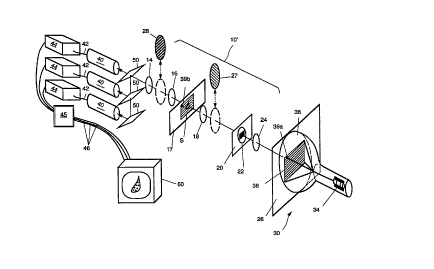
Referring now to figure lb, the transmitted light fluorescence im~ging
system according to the present invention is there illustrated and comprises
generally a means such as an optical system 10, a spot scanner means generally
indicated at 30 and means for sensing 40. In a further embodiment of the
invention the electrical output signal is tr~n~mittP~l to a video display device 60. A
digital processing device 45 may be used for computation and additional control
for display.
Referring now to figure 4, the spot scanner means takes the form of a
conventional cathode ray tube (CRT) 30. The CRT includes a glass envelope 32
~, 30 with a means for generating an electron beam or electron gun 34 positioned at one
end and a sub~t~nti~lly flat screen 36 that is coated with phosphor 38 which is
,- positioned at the opposite end. Individual phosphor spots 39 are excited as an
electron beam 35 sweeps in a raster pattern across the screen 36. The deflectionsystem 31 is adapted to scan in a raster pattern which comprises a predeterminPr1
CA 022349~0 1998-04-16
W O 97/16922 PCTAUS96/1750S
number of horizontal lines spaced vertically from each other a predetermined andequal distance. The electron beam 35 is adapted to sequentially excite the
phosphor 38 on the screen 36 in order to produce an illl~min~te-l spot 39 in theobject plane 26 of figures lb, 2b, and 3b that scans correspondingly in the raster
5 pattern. The phosphor 38 is chosen from among commercially available types
emitting the desired wavelengths. Standard phosphor emission spectra are
presented in various reference materials, including the Phosphor Resource Manualfor Industrial and Military Cathode Ray Tubes published by the Tm~ging and
Sensing Technology Corporation of New York.
For a detailed description of the operation of a CRT 30 the reader is
referred to any one of the numerous texts on the topic. Furthermore, the means for
generating the spot 30 may also comprise an electron beam such as is found in
electron microscopes, or a laser beam such as found in laser sc~nnin~ rnicroscopes.
The transmitted light im~ging system 10 of fig. lb also includes an optical
15 lens means or optical lens system 18, 24 for im~ging in a diffraction limite-l
m~nner, the object plane 26 on to the intermediate image plane 20, where a fieldstop 22 defines the field of view, and then im~ging the interrnediate image plane
20 onto the sample plane 17 such that the image 39b of tne spot 39a is the ~m~lle.st
diffraction limited size that can be created by the optical lens system 10. In its
20 simplest form, the optical lens system 10 substantially resembles the conventional
tr~n~mittetl light optical microscope 10 of figure la without the lamp 12.
Also included in the im~gin.~; system of the present invention is a means 40
for sensing the interaction of the spot 39b with a corresponding location on thesample S and for producing a modulated output signal proportional thereto. The
25 means 40 generally comprises one or more photomultiplier tubes (PMTs),
depending on the number of signal channels to be output.
Referring again to figure lb, according to the im~ging system of the present
invention if a CRT screen 36 is placed in the projection image plane 26, the image
of the sc~nning spot 39a is dem~gnified through the projection lens 24 and the
30 objective lens 18 and is focused onto the sample plane 17 so as to trace over the
sample S. The light transmitted through the sample S is collected by lens 16 and is
directed through the color filters 50 and the filtered light is input to the respective
photomultiplier tubes (PMTs) 40. The PMTs output electrical signals on lines 42
that are then input to signal amplifiers 44. The amplifier signals are tr~n~mitterl by
- 6-
CA 022349~0 1998-04-16
W O 97/16922 PCT~US96/17505
lines 46 to each of the red, green and blue inputs of a color display monitor 60thereby recreating the image of the scanned portion of sample S on the display
monitor 60. A digital processing device 45 may be used for computation and
additional control for display. In addition, the number of color detector channels
5 may be any reasonable value and the im~ging system may also be operated as a
black and white model using one PMT 40 and without the color filters 50 if a
particular application so requires
For fluorescence operation, excitation filter 27 is inserted into the
min~tion path before the objective lens 18, and emission filter 28 is inserted in
10 the sensing path generally after the condenser lens 16. The excitation filter 27
defines the bandwidths of radiation falling on the sample to excite fluorescence,
and the emission filter 28 defines the bandwidths of fluorescent emission allowed
to be passed to the sensing path. Single or multiple excitation and emisssion
bandwidths may be used as rletermined by commercially available filters.
The color filters 50 can be chosen for several different reasons: l) to divide
the received radiation into color wavelength bands suitable for full color display of
white light non-fluorescent images with filters 27 and 28 removed, 2) to define
distinct fluorescent emission wavelength bands to be used in conjunction with, or
in place of, emission filter 28, and 3) to define color wavelength bands that are
20 compatible with both fluorescent discrimin~tion in conjunction with filter 28 and
for white light separation for full-color display of non-fluorescent white lightilllln~in~tion with filters 27 and 28 removed. The last option is preferred for rapid
interchange of white light color im~ging and fluorescent im~ging.
25 Reflected light imaging system
In a conventional reflected light microscope shown in figure 2a, generally
indicated at 10, the lamp or bulb 12 ill~lmin~tes the sample S lying in a slide plane
17 through a relay lens 25, a partially tr~n~mittin~ and reflecting surface 29, and
an objective lens 18. From the reflected light leaving the sample, objective lens 18
30 creates an image S of the sample S in the intermediate image plane 20. The
diameter of the field stop 22, located in this plane, defines the field of view (FOV)
surrounding the sample image S . Lens 24 creates a projected image S of the
intermediate image S either in the eye, or directly onto a projection image plane
26, typically 25 cm from the projection lens 24. For white light viewing, the
-- 7 -
CA 022349~0 1998-04-16
W O 97/16922 PCT~US96/17505
partially tr~n~mittin~ and reflecting surface can be a simple beam splitter with the
same spectral b~n-lp~ in both optical channels.
For fluorescence operation, excitation filter 27 is inserted in the
illnmin~tion path, generally before the partially tr~n~mitting and reflecting surface
5 29f, and an emission filter 28 is inserted into the viewing path, generally between
the partially transmitting and reflecting surface 29f and the intermediate imageplane 20. The excitation filter 27 defines the wavelengths of radiation falling on
the sample to excite fluorescence, and the emission filter 28 defines the
wavelengths of fluorescent emission passed to the sensing path. Single or multiple
10 excitation and emisssion bandwidth filters may be used according to commercial
availability. The partially transmifflng and reflecting surface 29f is generally a
dichroic mirror, fabricated to reflect the excitation wavelengths and to tr~n~mit the
emission wavelengths. Operating in this m~nner, surface 29f aids the excitation
filter 27 and emission filter 28 in separating wavelengths and minimi7.ing cross15 taL~ between the excitation and emission bands.
According to the reciprocity rules of optical systems, an object placed in the
projection image plane 26 will be imaged backwards through the optics onto the
slide plane 17 with the lens m~gnification factors reversed.
Referring now to figure 2b, the reflected light fluorescence im~ging system
20 according to the present invention is there illustrated and comprises generally a
means such as an optical system 10, a spot scanner means generally indicated at
30 and means for sensing 40. In a further embodiment of the invention the
electrical signal from the sensing means 40 is tr~n~mitte-l to a video display device
60. A digital processing device 45 may be used to convert the signal to digital
25 form for computation and additional control for display.
The reflected light im~ging system 10 of figure 2b also includes an optical
lens means or optical lens system 18, 24 for focusing in a diffraction limite-l
m~nner, the object plane 26 on to a sample plane 17 such that the image 39b of the
spot 39a is the smallest diffraction limited size that can be created by the optical
30 lens system 10'. In its simplest form, the optical lens system 10' subst~nti~lly
resembles the conventional reflected light optical microscope 10 of figure 2a
without the lamp 12. However, the filters 27 and 28 are exchanged because the
min~tion and sensing paths are exhanged.
CA 022349~0 1998-04-16
W O 97/16922 PCTAUS96/17505
Also included in the im~ging system of the present invention is a means 40
for sensing the interaction of the spot 39b with a corresponding location on thesample S and for producing a modulated output signal proportional thereto. The
means 40 generally comprises one or more photomultiplier tubes, depending on
the number of color signals to be output.
Referring again to figure 2b, according to the im:~ging system of the present
invention if a CRT screen 36 is placed in the projection image plane 26, the image
of the sc~nning spot 39a is dem~gnified through the projection lens 24 and the
objective lens 18 and is focused onto the sample plane 17 so as to trace over the
10 sarnple S. The light reflected or emitted from the sample S is collected by lens 18
and is reflected by surface 29 through relay lens 25 to the color filters 50 and the
filtered light is input to the respective photomultiplier tubes (PMTs) 40. The
PMTs output electrical signals are transmitted through lines 42 and then input to
signal amplifiers 44. The amplifier signals are tr~n~mitt~fl by lines 46 to each of
15 the red, green and blue inputs of a color display monitor 60 thereby recreating the
image of the scanned portion of sample S on the display monitor 60. In addition,the number of color detector channels may be any reasonable value and the
im~ging system may also be operated as a black and white model using one PMT
40 and without the color filters 50 if a particular application so requires.
For fluorescence operation, excitation filter 27 is inserted into the
min~tion path before the partially tr~n~mitfin~ and reflecting surface 29f, and
emission filter 28 is inserted in the sensing path generally after the partiallytransmitting and reflecting surface 29f, The excitation filter 27 defines the
wavelengths of radiation falling on the sample to excite fluorescence, and the
25 emission filter 28 defines the wavelengths of fluorescent emission passed to the
sensing path. Single or multiple excitation and emisssion bandwidths may be usedaccording to the commercial availability of filters.
The color filters 50 can be chosen for several different conditions: 1) to
divide the incident radiation into color wavelength bands suitable for full color
30 display of white light non-fluorescent images with filters 27 and 28 removed, 2) to
define distinct fluorescent emission wavelengths to be used in conjunction with or
in place of emission filter 28, and 3) to define spectral wavelengths that are
compatible with both fluorescent discrimin~tion in conjunction with filter 28 and
for white light separation for full-color display of non-fluorescent white light
CA 022349~0 1998-04-16
W O 97/16922 PCT~US96/17505
illllmin~tion with filters 27 and 28 removed. The last option is preferred for rapid
interchange of white light color im~ging and fluorescent im~ging.
Combination Transmitted and Reflected light imaging system
S Some conventional microscopes can be operated in either a reflected or
tr~n~mitted light mode shown in figure 3a by combining the elements of figures la
and 2a. The system requires two lamps, one for the tr~n~mitte-l light path 12T and
one for the reflected light path 12R and a removable holder for the filters 27 and
28 and the partially tr~n~mitting and reflecting surfaces 29 and 29f. There is only
10 one image sensing path through projection lens 24 to the eye or a projection
screen.
For tr~n~mitte.d light operation, the reflecting and tr~n~mitting surfaces 29
and 29f and the emission filter 28 are removed from the optical path. Lamp 12T is
used for illnmin~tion and lamp 12R is off. Figure 3a does not show transmitted
15 light fluorescence components since this technique has been abandoned by
equipment m~nllf~rtllrers.
For reflected light operation, lamp 12R is used for illnmin~tion and lamp
12T is off. The partially reflecting and tr~n.~mitting surface 29 is inserted into the
optical path. For fluorescence operation, the excitation filter 27 and the emission
20 filter 28 are inserted into the optical path in addition to the partially reflecting and
tr~n~mitting surface 29f.
Referring now to figure 3b, the combination tr~n~mitte~l and reflected white
light and fluorescence im~ging system according to the present invention is there
illustrated and comprises generally a means such as an optical system 10, a spot25 scanner means generally indicated at 30 and means for sensing transmitted light
40T and a means for sensing reflected light 40R. In a further embodiment of the
invention the electrical output signal is transmitted to a video display device 60. A
digital proces~in~ device 45 may be used to combine the reflected and transmitted
path signals and convert the signals to digital form for computation and additional
30 control for display
Transmitted light operation
The tr~n~mitt~-~l light im~gin~ portion of figure 3b also includes an optical
lens means or optical lens system 18, 24 for im~in~ in a diffraction limited
- 10-
CA 022349~0 1998-04-16
-
W O 97/16922 PCTrUS96/1750~
m~nner, the object plane 26 on to the intermediate image plane 20, where a fieldstop 22 clefinPs the field of view, and then im~ging the interm~diate image plane
20 onto the sample plane 17 such that the image 39b of the spot 39a is the smallest
diffraction limite-l size that can be created by the optical lens system 10 .
Also included in the im~ging system of the present invention is a means
40T for sensing the interaction of the spot 39b with a corresponding location onthe sample S and for producing a mo-llllAtPd output signal proportional thereto.The means 40T generally comprises one or more photomultiplier tubes, depending
on the number of signal channels to be output.
Referring again to figure 3b, according to the imaging system of the present
invention if a CRT screen 36 is placed in the projection image plane 26, the image
of the sc~nning spot 39a is dem~gnified through the projection lens 24 and the
objective lens 18 and is focused onto the sample plane 17 so as to trace over the
sample S. The light transmitted through the sample S is collected by lens 16 and is
1~ directed through the color filters 50T and the filtered light is input to the respective
photomultiplier tubes (PMTs) 40T. The PMTs output electrical signals on lines
42T that are then input to signal amplifiers 44T. The amplifier signals are
tr~n~mittP-l by lines 46T to each of the red, green and blue inputs of a color display
monitor 60 thereby recreating the image of the scanned portion of sample S on the
display monitor 60. A digital processing device 45 may be used for computation
and additional control for display. In addition, the number of color detector
channels may be any reasonable value and the im~ging system may also be
operated as a black and white model using one PMT 40T and without the color
filters 50T if a particular application so requires.
For fluorescence operation, excitation filter 27 is inserted into the
min~tion path before the objective lens 18, and emission filter 28T is inserted
in the sensing path generally after the condenser lens 16. The excitation filter 27
defines the bandwidths of radiation falling on the sarnple to excite fluorescence,
and the emission filter 28T ~lefines the bandwidths of fluorescent emission allowed
to be passed to the sensing path. Single or multiple excitation and emisssion
bandwidths may be used as determined by commercially available filters.
The color filters 50T can be chosen for several different reasons: 1) to
divide the received radiation into color wavelength bands suitable for full color
display of white light non-fluorescent images with filters 27 and 28T removed, 2)
CA 022349~0 1998-04-16
W O 97/169~2 PCTAJS9G/17505
to define distinct fluorescent emission wavelength bands to be used in conjunction
with, or in place of, emission filter 28T, and 3) to define color wavelength bands
that are compatible with both fluorescent discrimin~tion in conjunction with filter
28T and for white light separation for full-color display of non-fluorescent white
S light illllmin~tion with filters 27 and 28T removed. The last option is preferred for
rapid interchange of white light color im~ging and fluorescent im~gin~.
Reflected light operation
The reflected light portion of the im~ging system 10 of figure 3b also
10 includes the optical lens means or optical lens system 18, 24 for focusing in a
diffraction limit~1 manner, the object plane 26 on to a sample plane 17 such that
the image 39b of the spot 39a is the smallest diffraction limited size that can be
created by the optical lens system 10 .
Also included in the im~gin~ system of the present invention is a means
lS 40R for sensing the interaction of the spot 39b with a corresponding location on
the sample S and for producing a mo~ t~ output signal proportional thereto.
The means 40R generally comprises one or more photomultiplier tubes, depending
on the number of color signals to be output.
Referring again to figure 3b, according to the im~ing system of the present
20 invention if a CRT screen 36 is placed in the projection image plane 26, the image
of the sc~nning spot 39a is dem~gnified through the projection lens 24 and the
objective lens 18 and is focused onto the sample plane 17 so as to trace over the
sample S. The light reflected or emitted from the sarnple S is collected by lens 18
and is reflected by surface 29 through relay lens 25 to the color filters SOR and the
25 filtered light is input to the respective photomultiplier tubes (PMTs) 40R. The
PMTs output electrical signals are tr~n~mitted through lines 42R and then input to
signal amplifiers 44R. The amplifier signals are transmitted by lines 46R to each
of the red, green and blue inputs of a color display monitor 60 thereby recreating
the image of the scanned portion of sample S on the display monitor 60. In
30 addition, the number of color detector channels may be any reasonable value and
the im~ging system may also be operated as a black and white model using one
PMT 40R and without the color filters 50R if a particular application so requires.
For fluorescence operation, excitation filter 27 is inserted into the
min~tion path before the partially transmitting and reflecting surface 29f, and
- 12-
CA 022349~0 1998-04-16
W O 97/16922 PCTAUS96/17505
emission filter 28R is inserted in the sensing path generally after the partially
transmitting and reflecting surface 29f, The excitation filter 27 defines the
wavelengths of radiation falling on the sample to excite fluorescence, and the
emission filter 28R defines the wavelengths of fluorescent emission passed to the
sensing path. Single or multiple excitation and emisssion bandwidths may be usedaccording to the commercial availability of filters.
The color filters 50R can be chosen for several different conditions: 1) to
divide the incident radiation into color wavelength bands suitable for full color
display of white light non-fluorescent images with filters 27 and 28R removed, 2)
10 to define distinct fluorescent emission wavelengths to be used in conjunction with
or in place of emission filter 28R, and 3) to define spectral wavelengths that are
compatible with both fluorescent discrimin~tion in conjunction with filter 28R and
for white light separation for full-color display of non-fluorescent white lightill-lmin~tion with filters 27 and 28R removed. The last option is preferred for
15 rapid interchange of white light color im~gin~ and fluorescent im~gin~.
It has been emphasized herein that the im~ging system according to the
present invention operates at the diffraction limit of the optics (or more
particularly the microscope) to which it is attached. It is believed by the applicant
that heretofore no such im~ging system has been devised. By operating at the
20 diffraction limit advantages occur, namely resolution is signific~ntly enhanced. In
addition, the im~ging system of the present invention has the ability to zoom in on
the sample and to enhance or suppress the output signal in order to modify the
detectability of a portion of the sample. In addition, by combining the
transmission and reflection modes by the insertion or removal of combinations of25 the partially transmitting and reflecting surfaces 29 and 29F, and the filters 27,
28T and 28R, the im~gin~ system of the present invention can operate as:
1) a white light tr~n~mi~ion or reflection system,
2) a white light tr~n~mi~ion and reflection system,
3) a fluorescence tr~n~mi~ion or reflection system,
4) a fluorescence tr~n~mi~ion and reflection system
S) a nonfluorescence tr~n~mitte~l and fluorescence reflection system,
6) a tr~n~mitte~l fluorescence and nonflourescence reflection system.
CA 022349~0 1998-04-16
W O 97/16922 PCT~US96/17505
With the foregoing in mind, in the discussion which follows the reader will
come to understand the physical parameters of the present im~ging system.
Relationship between the CRT spot and raster size,
and microscope optical components 7
In order to achieve diffraction-limited resolution of spot 39 (fig. lb), the
CRT spot radius is ~letermine~l by the diffraction limit of the optics. The scanned
field size is determined by the diameter of the field stop 22 in the intermediate
image plane 20. Table 1 shows the diffraction-limitP~l spot sizes in the three image
10 planes of a conventional microscope for a typical selection of objective powers 18.
Column (8) is the number of diffraction-limite~i picture elements across the field of
view.
Table 1. The Optical Specifications of a Conventional Microscope
(1) (2) (3) (4) (5) (6) (7) (8)
FOV Eyep. Obj. Obj. Ro R 1 R2 Elem
(mrn) Ma~. Ma~. NA (lUm) (Llm) (~Im) FOV
0.30 1.12 1 1.18 1 1 1.8 1785
0.75 0.45 17.89 178.9 1 1 18
100 1.30 0.26 25.81 258.1 775
Ro is the radius of the smallest resolvable element in the slide plane 17 (~lg.
lb) calculated from the Rayleigh resolution criterion.
(1) Ro=0.61 ~/NA,
where ~ = 550 nm is the chosen wavelength representing the center of the visible
spectrum, and NA is the nllmeric~l aperture of the objective lens 18.
The radius of the image of Ro in the intPrmediate image plane 20 between
the objective 18 and the eyepiece lens 24 is
(2) R1 = Ro x Mag obj
- 14-
CA 022349~0 1998-04-16
W O 97/16922 PCTAJS96/17505
In the intermP.~ te image plane 20, the field stop 22 defines the diameter of
the field of view for the whole system, Fl = FOV = 20 mm in this example. The
radius of the image of R 1 in the projection image plane 26 is
(3) R2 = Rl xMageye -
At the location of the projection image plane 26, a real image can be shown
on a screen. The diameter of the field of view in the projected image plane is
(4) F2 = Fl xMageye,
and the diameter of the field of view in the slide plane 17 is
Fl
(S) Fo = Mag eye
While this discussion refers specifically to a microscope having a fixed
eyelens power and a fixed intermediate image plane field stop size, such
conventions are artificial, and not meant to be limiting on the present invention.
The number of resolved elements across the field of view for each objective
20 lens 18, shown in column (8) is
Fo FOV F2
(6) N = R0 = R 1 R2
N is therefore a function of the numerical a~elLule of the objective lens 18 and the
25 diameter of the field stop in the int~rmediate image plane 20.
From the table, the maximum number of resolved elements is 1785, which
occurs for the lowest m~gnification option. The smallest point radius in the
projected image plane is R2 = 111.8 mm from column (7), which also occurs for
the lowest m~gnification option. The projected image field diameter is F2 = 20 cm
30 from equation (4), and is constant for all objective m~gnification options.
In order to insure diffraction-limited resolution for all optical powers, the
scanner CRT 30 must produce a spot radius less than or equal to the smallest value
-- 15 -
CA 022349~0 1998-04-16
W O 97/16922 PCT~US96/17505
of R2 in the table. In order to match the field of view of the microscope, the scan
area on the CRT 30 must be comparable to F2. Since video sc~nning patterns 12
have a rectangular shape (raster scan) and a typical microscope field of view iscircular, the diagonal of the scanned pattern should match the circle diameter, F2.
5 The eyepiece field stop 22 could also be fabricated in a rectangular shape to match
the CRT scanned pattern. A random sc~nning pattern could also be employed for
tracing edges of samples and other specialized functions, but the basic
geometrical-optical relationships for diffraction-limited resolution and full field
display remain the same. It will therefore be noted that the aspect ratios of the
10 scan p~ttPnl~ on the CRT 30 and the display monitor 60 must be the same, whether
4:5, 3:4, 1: l, or any other desired value.
Relationship between phosphor decay time and raster scan rates
A common manner of determining the contrast of an optical system such as
15 system 10' is to use a sample consisting of a field of parallel black and white bars
of the same width. Theoretically, the black bars have 0% transmission, and white(or clear) bars have 100% tr~n~mi~ion. As the spot is traced perpendicular to the
bars, the modulation of the transmitted light signal may be determined from the
formula~0
max signal - min signal
(8) Modulation = max signal + min signal
which is also referred to as the image contrast. The reader is referred to classical
texts, such as Chapter 11 of Modern Optical Engineering, McGraw Hill, 1966, by
25 Warren Smith. The signal modulation is measured for decreasing bar widths and a
graph of the modulation vs. bar width, or resolution, can be drawn. For this
example, the modulation for a diffraction-limite~l spot tracing a diffraction-limite~l
bar width is desired. The modulation for these conditions is a function of the scan
speed and the phosphor decay characteristics. The relationship will now be
30 derived.
All CRT phosphors exhibit a decrease in intensity after excitation by the
electron beam 35. The decay period is normally defined as the time interval in
which the phosphor intensity decreases to 10% of the initial intensity.
- 16-
CA 022349~0 1998-04-16
W O 97/16922 PCTAJS96/17505
Occasionally, a 1% phosphor intensity is used to define decay time. Decay times
and decay curve shapes vary widely between phosphor types and operating
conditions. Mathematical representations of decay curves include exponential andpower law formulas, but are generally not known. Usually, measured curves are
5 the only representations available.
A specific relationship exists between the scan rate of the flying spot 39 and
the contrast of the image. The scan rate determines the pixel dwell time, or theresidence time of the optical spot over a single resolution element. The word pixel
usually means a "picture element", but as used here means a "diffraction-limited10 picture element", whose dimension is defined in eqn. (1). If the spot 39a scans
rapidly across the screen 36 so that the pixel dwell time is much shorter than the
phosphor decay time, then previous resolution elements will continue emitting
light after the electron beam 35 has passed. The result is a reduction in contrast of
the signal.
The effects can be illustrated by figures S and 6. Figure 5 represents a
norm~li7~.-1 phosphor decay curve showing brightness versus time. Let us choose
the pixel dwell time as 1/4 of the total decay time and divide the curve into four
equal time zones. The area in each zone is shown in the table at right and
represents the total light flux emitted during that time interval. Figure 6, case a
shows successive positions of the light spot during the four time zones as it scans
over a set of parallel black and white bars whose width is the diffraction limit of
the optics. Each spot position represents one pixel dwell time. Figure 4, case bshows case a one pixel dwell time later. Case a and case b represent the m~ximllm
and minimllm signal states of the position of a sc~nning spot tracing over the bars
for the given pixel dwell time. The ill-lmin~tion of pixels 1, 2, 3, and 4 will be
fractions of the decay curve as shown. The total light transmitted through the
sample will be the sum of the light flux illllmin~ting each pixel times the
tr:-n~mi~ivity of each pixel, which was defined as either black (0% tr~n~mi~ion),
or white (100% tr~n~mi~ion).
For this example, the image modulation, or contrast, that follows from the
two states is 0.5195, or 51.95%. Any pixel dwell time could be used in the
example, and the procedure repeated to determine the resulting contrast. It is
common practice in the design of optical im~ging systems to specify that the
image modulation shall be greater than 50% at the specified resolution. Design
- 17-
CA 022349~0 1998-04-16
WO 97/169Z2 PCT/US96/17505
values down to 30% may be adequate. The limit of visual detection occurs at
image modulation values in the range of 2-3.5%.
The direct interaction between the sG~nnin~ spot 39b and the sample S is
the only interaction that relates the phosphor decay time to the pixel dwell time.
S More sophisticated calculation methods may be employed, but adequate values can
be achieved with this simple method. The contrast is also affected by scattering or
other effects away from the sample S.
The horizontal and vertical scan times of the raster on the CRT 30 are
detPrmined from the pixel dwell time. The horizontal scan period is
(7) Th = txNh+th,
where t = pixel dwell time,
Nh = number of horizontal pixels,
and th = h~ ri7o~t~1 bl~nkin~ time.
The horizontal scan frequency is then
(8) Wh = Th-l .
The vertical scan period is
(9) Tv = ThXNv+tv,
where Th = horizontal scan period from eqn. (7),
Nv = number of verticalpixels,
tv = vertical bl~nkin~ time.
The vertical scan frequency is then
(10) Wv = TV-1 .
At this point, the following parameters have been defined: the phosphor
spot size that will yield the smallest diffraction-limited spot 39b on the sample
- 18-
CA 022349~0 1998-04-16
W O 97/16922 PCTAUS96/17505
plane 17 for all objective powers; the scan rates that will yield a predetermined
contrast for a diffraction-lirnited pixel; and a scan raster size that will illllmin~te a
full field of view.
- 5 Frequency response of the detector circuits
The next component of the im~ging system requires the conversion of
optical information into electronic information. The procedures above insure that
the pixel data is being generated at maximum resolution with good contrast.
The light that is transmitted, reflected, or emitted from the sample that falls
on the photomultiplier tubes is characterized by a rapidly varying intensity level
resulting from the varying absorptivity, reflectivity, or emissivity at each point on
the sample. In order to preserve the resolution, the means for sensing or PMTs 40
and associated amplifiers, must be able to create an electrical signal that faithfully
reproduces the amplitude and frequency of the rapid fluctuations in intensity of the
light from the sample. The minim~lm frequency response must match or exceed
the inverse pixel dwell time. Electronic circuit frequency response is usually
stated in terms of a graph of frequency vs. modulation amplitude in a manner very
similar to the optical modulation/contrast definition given above. Typical
specifications give the frequency response at 3 dB roll-off, or 50% modulation. If
the optical modulation at the slide is 50~o, and the electrical amplifier modulation
is 50%, the resultant signal has a modulation of 25%, which would approach a
design minimum. The frequency response could be specified at 1 dB (79%), or 0
dB roll-off for better modulation and higher fidelity to the incoming signal. The
reader will note that PMTs are well known in the art and therefore it is not
necessary to describe specific PMTs or amplifier circuits, but rather to describe the
conditions for the proper operation thereof in the particular image system of the
present invention. Frequency bandwidths of 20 MHz and up are typical,
exceeding the 3.75 MHz bandwidth of ordinary television standards by a
significant amount. According to the conditions outlined above, standard
television scan rates and amplifier bandwidths cannot approach the diffraction-
limite~l requirements of an conventional microscope image.
- 19-
CA 022349~0 1998-04-16
W O 97/16922 PCTAUS96/17505
Resolution and contrast of the display monitor
The signals from the PMT amplifiers 44 on lines 46 contain all the
information available from the im~ging system. The arnplified output signals canbe displayed directly on a video display 60, or digitized and output to a digital
5 processing device or other permanent storage media for display, analysis, or
telecommunication. The specifications of the display monitor 60 determine the
final visual quality of the image. If the monitor 60 can display the number of color
pixels contained in the signal from the video amplifiers 44, then the resolution and
the field of view of the ordinary microscope image can be reproduced. The
10 monitor's video amplifier bandwidth and phosphor characteristics will determine
the monitor's resolution and contrast, and hence its ability to faithfully represent
the original electronic output signals from the microscope video ampli~lers 44. For
monitors with fewer pixels than contained in the video signal from the im~ging
system, a trade-off between field of view and resolution can be made, resulting in
15 full resolution in a ~m~ller field of view.
Zoom mode
The display screen of the monitor 60 represents a constant size window
showing the contents of the scanned area on the slide. If the scanned area on the
20 slide is made ~m~ller, it is still displayed full size on the monitor 60, giving a
m~nification zoom effect. In other words, varying the size of the raster pattern on
the spot sc~nning device causes the raster on the sample to be correspondingly
changed thereby c~ inf; a larger or .cm~ller portion of the sample to be contained
within the output signal providing a variable m~gnific~tion to the display device or
25 other signal proces~ing device. When used with lower power objectives 18 thathave a large number of pixels in the field of view, any area can be zoomed in
m~gnification so that the display resolution matches the diffraction limit of the
optics. For example, if there are 1700 pixels across the microscope image, and
only 1200 pixels across the monitor screen, then the zoom feature can be used to30 shrink the raster down to cover only 1200 pixels on the sample so the resolution of
the display 60 matches or exceeds the image resolution at the reduced field of
view.
- 20-
CA 022349~0 1998-04-16
W O 97/16922 PCTrUS96/17505
Another characteristic of the zoom feature is constant brightness in the
image for any zoom m:~gnification setting. The brightness of the raster on the
scanner CRT 30 is given by the relation
(12) Bp = kx A
-
where I is the electron beam current, A is the area of the scanned raster, and k is a
constant factor. The subscript p refers to the phosphor 38. Equation (12) is linear
over a wide range of beam current settings. When the sc~nn~-l area is re~ ce-l for
10 constant beam current, the brightness increases in inverse proportion to the area
change.
If the m~gnification of an optical system is changed, such as ch~ngin~
objective lenses 18 in a microscope, then the light passing through the lens system,
and hence the brightness of the image is changed in direct proportion to the area
15 change of the image. The brightn~ss change can be represented by the relation
(13) Bl = Bo x A,
where Bo is the initial image brightness. If Bo comes from a phosphor satisfying20 eqn. (12), then eqn. (13) becomes
(14) B = [k x A] x A = k x I
Equation (14) shows that a change in m~gnification due to changing the
25 raster size has no effect on the brightness of the image. The variation in phosphor
brightness exactly compensates for the variation in area. Since the mechanical
system is not altered, the focus does not change. The zoom feature therefore
produces a change in m~gnification with no change in brightness or focus.
Contrast enhancement or suppression by spot modulation
In all current sc~nning type microscopes, the spot brightness is constant as
it travels over the sample S. Mo~ ting the spot brightness as a function of image
content can be a powerful tool for image clet~iling Spot modulation requires that
- 21 -
CA 022349~0 1998-04-16
W O 97/16922 PCTAJS96/17S05
the scanner CRT 30 circuits include a video amplifier and driver capable of
mo~ tin~ the electron beam at a frequency bandwidth no less than the PMT
amplifier circuits 44.
If the spot brightness is decreased as it traces over a dark object, the
S resultant signal will show an enhanced dark swing. The feature may elimin~te in
many applications the need for conventional microscope contrast enhancement
accessories (such as "differential interference contrast", darkfield illllmin~tion,
and other phase contrast components) while m~int~ining full image resolution.
This mode is called contrast enhancement, or positive feedback, or normal signal10 mode.
Conversely, if the spot bri~htn~.s~ is increased as it traces over a dark object,
the signal will show a reduced dark swing, or possibly no dark swing at all. This
mode is called the contrast suppression, or negative feedback, or inverted signal
mode. In the contrast suppression mode, portions of images can be made to
15 disappear, or become much less prominent.
The signal used to modulate the scanner CRT 30 brightness is derived from
the actual sample image signal from one or more of the PMT channels. The signal
from a single channel may be used in either the normal or inverted mode, or
several channels may be mixed and used in normal or inverted mode. In this
20 manner, colored objects in the image may be selectively enhanced or suppressed.
For example, in the ex~minAtion of a blood smear, the combination of
colors for red blood cells could be fed into the scanner CRT video amplifier in a
negative feedback mode to suppress or ~limin~t~ red blood cells from appearing in
the image. This is not a data processing feature that works on the output image
25 data, but a feature that is operative during creation of the image. Any colorchannel, or combination of color channels could be combined and used as positiveor negative feedback to the scanner CRT.
The foregoing spot intensity modulation can also be applied to laser and
eiectron beam im~gin~ systems.
CA 022349~0 1998-04-16
W O 97/16922 PCTAUS96/17505
An Example
To illustrate the previous description of the invention, a specific example will now
be described.
- 5 a) CRT spot size and raster size. The information in Table 1 andsurrounding equations describe a conventional microscope optical system. The
information in that section defines the following:
Smallest CRT spot size radius = 111.8~m,
CRT raster size = 20 cm diagonal.
The CRT envelope, gun structure, and high voltage are specified in combination to
meet the specification. Many combinations are available to one skilled in the art.
This example assumes a 3:4 raster aspect ratio.
b) Phosphor decay time and raster scan rate. The faster the phosphor
decay time, the faster the scan rate. In general, a very fast phosphor is required for
a scan rate fast enough to allow direct viewing on a video monitor. Phosphors inthe P46 family have 1% decay times of approximately lOOns. Assume the pixel
dwell time is chosen to be 1/3 the phosphor decay time, or 33ns. for a 1024 x 768
pixel monitor, the horizontal period from equation (7) is
Th = t x Nh + t h = 33 ns x 1024 + 6 ~IS
= 39.8,us,
where the bl~nking time was chosen to be 6 ~s. The horizontal frequency is 25
25 kHz. The vertical period from equation (9) is
Tv= ThxNv+t~,=39.8nsx768+10ms
= 38.6 ms,
30 where the vertical bl~nking time is chosen as 10 ms. The vertical frequency is
25.9 Hz. In order to avoid objectionable flicker in a directly viewed image, a
display monitor with long persistence phosphors may be required.
CA 022349~0 1998-04-16
W O 97/16922 PCTAJS96/17505
c) Video amplifier bandwidth. For a pixel dwell time of 33 ns, a minimllm
amplifier bandwidth of 30.3 MHz+ 1 dB is required. The video amplifiers in the
display monitor must have at least the same bandwidth to m~int~in the resolutionof the signal.
From table 1 it can be seen that the field of view and resolution of the
display monitor match direct viewing in the conventional microscope above about
40x objective power. For the lOx objective, the image must be zoomed to
approximately 1024/1785 = 57% of full field for the monitor to display the full
resolution of the optical system. At lOOx objective power, the monitor can display
10 more pixels than the optical system can resolve.
d) Fluorescence. P46 phosphor contains blue and green spectral bandwiths
suitable for excitation of common fluorescent bands useful in biomedical
applications. This example refers to the popular fluorochrome systems using
15 excitation in the 515 - 560nm range, with fluorescent emission above 590nm. This
excitation region is used for TRITC (tetramethlyrho~l~mineisothiocyanate), Evansblue, Rhorl~min~ B 200, Pararos~nilin~, Thi~7.in~- red R, Xylene orange, and Acid
fuchsine. The samples were existing laboratory slides of rhizomes and a mouse
embryo section approximately lO,um thick. The slides and had no special
20 treatment for fluorescence, so autofluorescent emission was observed. In the
transmitted light mode, the excitation filter was placed above the objective lens
and the emission filter below the condenser. The red channel of the three color
sensing path was used. The three full color filters ~iO were left in place. The
radiative power from the CRT screen in the excitation band entering the projection
25 lens was 45.59 ~lW. Fluorescent Images of the 10 ,um thick mouse embryo slidecould be achieved at 12Hz, suitable for focusing and scSlnning. Averaging 12
frames yielded a usable image.
The foregoing embodiments and examples are to be considered illustrative,
rather than restrictive of the present invention, and those modifications which
30 come within the me~ning and range of equivalence of the claims are to be included
therein.
- 24-