Note: Descriptions are shown in the official language in which they were submitted.
CA 02235355 1998-04-20
"SUPPLY CIRCUIT FOR DISCHARGE LAMPS WITH OVERVOLTAGE
PROTECTION"
F~P~d of the invention
The present invention relates to a supply
circuit with inverter for discharge lamps. More
particularly the present invention relates to a supply
circuit for discharge lamps with heated electrodes, in
which an inverter comprising controlled breakers,
turned on and off alternately, supply a load circuit
having at least one lamp and an LC resonant circuit in
series with the lamp.
State of the art
Systems for controlling the voltage on the
electrodes of the lamp and which have the objective of
modifying the behaviour of the load circuit or of
turning off the supply thereto in case of defective
operation of the lamp, are often used in supply
circuits of the type mentioned above, with the
objective of preventing excessively high voltages from
arising between the electrodes.
From EP-A-0 610 642 there is known a supply
circuit with inverter for discharge lamps, in which
associated with the load circuit is a control circuit
comprising a voltage-dependent resistor (VDR) in series
with a dissipative element. When the voltage at one
terminal of the VDR exceeds a threshold value (which
occurs for example in the case of failure of the lamp
to light following a defect therein), the VDR becomes
conducting with the consequence that the resonant
circuit in series with the lamp receives an additional
dissipative element. This modifies the quality factor
of the circuit and hence reduces the voltage at the
terminals of the lamp. Provision is further made for a
timer circuit which turns off the supply to the load
circuit should the overvoltage condition last for a
time greater than a preset threshold value.
CA 02235355 1998-04-20
T
From EP-A-0 113 451 there is known a different
overvoltage control system, in which a voltage-
dependent resistor (VDR) in series with a capacitor are
inserted in parallel with a branch of the load circuit.
In this case when a voltage difference greater than a
specified threshold value is generated between the
terminals of the VDR, it becomes conducting and inserts
an auxiliary capacitor into the load circuit, modifying
the frequency of resonance of the resonant circuit in
series with the lamp.
Traditional circuits for protection from
overvoltages come into operation when the voltage
between the electrodes of the lamp exceeds a threshold
value. In the case of a defective lamp, and hence of
the failure of this lamp to light, the voltage between
the electrodes of the lamp reaches values of the order
of 1000 V. Conversely, when the lamp is removed from
the load circuit the potential difference between the
electrodes is of the order of 700 V. The circuits
currently available are unable to discriminate between
these two voltage values; which may moreover vary from
one instance to another of the circuit. Consequently
they cut in anyway, turning off the supply, a
prespecified time (of the order of 300 ms) having
elapsed from the onset of the establishment of a
situation of overvoltage between the electrodes of the
lamp and are unable to distinguish between the two
conditions of fault and lamp absent.
It would, on the other hand, be appropriate to
make provision for a circuit which is able to
discriminate between a .,situation of actual defective
operation and a situation of lamp absent in the load
circuit, in such a way that the substitution of the
lamp does not entail the disabling of the supply
inverter of the load circuit. Thus, in currently known
circuits the disabling of the supply inverter is
permanent and hence requires the intervention of the
operator in order to reactivate the supply for the
lamp, even when the disabling has occurred through
CA 02235355 1998-04-20
r
simple substitution of the lamp rather than through a
defect in operation thereof. On the other hand, in case
of overvoltage due to a defect in the operation of the
lamp in the load circuit there flows a high current,
which passes through the capacitor in parallel with the
lamp. This anomalous condition may lead to the
overstressing of the inverter and hence to damage
thereto. Protection from overvoltage has the objective
of preventing this consequence. When,.conversely, the
voltage in the load circuit increases on account of the
lamp being absent, the current which flows in the
circuit is practically zero and hence the inverter does
not experience the dangerous stresses which occur under
conditions of faulty lamp. Disabling of the inverter is
therefore superfluous.
Summary of the invention
The objective of the present invention is the
construction of a supply circuit for discharge lamps,
with an overvoltage protection system, not exhibiting
the drawbacks of the traditional circuits briefly
described above.
More particularly the objective of the present
invention is the construction of a supply circuit for
discharge lamps with an overvoltage protection circuit
which is able to discriminate between the conditions of
failure to light on account of defective lamp and the
conditions of lamp absent, and which cut off the supply
only when necessary, i.e. iri the case of defective
lamp.
Essentially, starting from a supply circuit of
the type defined above, the objectives indicated above,
and other objectives and advantages which will become
clear to those skilled in the art by reading the text
which follows, are achieved by making provision for the
overvoltage control circuit to comprise a band-pass
filter centred on the switching frequency of the
inverter, the input signal of which is dependent on the
voltage at a specified point of the load circuit and
the output signal from which is sent to control means
CA 02235355 1998-04-20
r
- 4 -
associated with the inverter so as to turn off the
supply for the load circuit in the case of defective
operation.
The invention is based on the observation that,
although the amplitude of the voltage between the
electrodes of the lamp is of the same order of
magnitude both-in the case of defective operation and
in the case of lamp absent, the waveform of the voltage
signal is, conversely, qualitatively different in the
two cases. In case of failure to light through a defect
in the lamp, the voltage between its electrodes has a
substantially sinusoidal profile with a frequency
corresponding to the switching frequency of the
inverter. In case of lamp absent, conversely, the
waveform of the voltage signal at the terminals of the
lamp exhibits, as well as a relatively limited
component at the switching frequency, a strong -signal
content at the higher harmonics:
By detecting this voltage signal and filtering
it through a band-pass filter centred on the switching
frequency, a signal, which will be a high signal when
the overvoltage established between the electrodes is
due to defective operation of the lamp inserted into
the load circuit, is therefore obtained at the output
of the band-pass filter. This signal will, conversely,
be low when the overvoltage established between the
electrodes is due to lamp absent. In this last case, in
fact, the signal component at~ the switching frequency
is of modest strength with respect to the components at
the higher harmonics, which are blocked by the band-
pass filter.
The control circuit thereby becomes capable of
discriminating between the conditions of defective
operation and the conditions of lamp absent and will be
able, with suitable logic, to intervene on the supply
inverter, selectively disabling the operation thereof.
Further and advantageous characteristics and
embodiments of the circuit according to the invention
CA 02235355 2004-02-16
2033:3-423
are indicated in the appended claims and will be described
in greater detail below.
In particular, a voltage divider, to which the
band-pass filter is linked, can be arranged in parallel with
5 a branch containing at least one component of the load
circuit (for example the inductive component). More
particularly the voltage divider can be placed in parallel
with a branch comprising one of the controlled breakers of
the inverter and the inductive component of the resonant
circuit in series with the electrodes of the lamp.
The band-pass filter can consist, in a
particularly simple embodiment, of an LC cell in parallel,
with a resonant frequency corresponding to the switching
frequency of the inverter.
According to one broad aspect the invention
provides a supply circuit for discharge lamps comprising: an
inverter for supplying the lamps with a supply voltage; a
load circuit connected to the inverter for receiving the
supply voltage; a filter connected to the inverter for
receiving the supply voltage and creating a filtered signal
representing only a portion of the supply voltage; a control
circuit connected to the filter for receiving and monitoring
the filtered signal and causing the inverter to turn off the
supply voltage provided to the load circuit in the case of a
defective lamp.
According to another broad aspect the invention
provides a method for disabling an electronic ballast from
providing a voltage to a defective lamp, the method
comprising: a. supplying a voltage from an inverter to a
load circuit; b. providing a voltage from the load circuit
CA 02235355 2004-02-16
2033<3-423
5a
to a control circuit; c. filtering the voltage provided to
the control circuit through a band-pass filter centered on
the switching frequency of the ballast to generate a
filtered signal at the output of said band-pass filter;
d. comparing the filtered signal with a predetermined
voltage; and e. disabling the inverter from providing a
supply voltage when the voltage received from the load
circuit is greater than the predetermined voltage.
According to yet another broad aspect the
invention provides a method for disabling an electronic
ballast from providing a voltage to a defective lamp, the
method comprising: a, filtering the voltage through a band-
pass filter centered on the switching frequency of the
ballast to generate a filtered signal at the output of said
band-pass filter; b. comparing the filtered signal with a
predetermined voltage; and c. disabling an inverter of the
electronic ballast from providing a supply voltage when the
filtered signal is greater than the predetermined voltage.
According to still another broad aspect the
invention provides a control circuit for a ballast supplying
a supply signal to a discharge lamp connectable to a pair of
lamp terminals comprising: a, an input circuit electrically
connected to at least one of the lamp terminals; b. a
sensing circuit electrically connected to the input circuit,
the sensing circuit producing a sensing output responsive to
a magnitude of a frequency component of the supply signal
that varies in accordance with whether the discharge lamp is
connected to the lamp terminals; and c. an output circuit
electrically connected to the sensing output and having an
output signal connected to the ballast that varies in
accordance with whether the discharge lamp is connected to
the lamp terminals.
CA 02235355 2004-02-16
, ~ 2033.3-423
5b
Brief description of the drawings
The invention will be better understood by
following the description and attached drawing, which shows
a practical and non-limiting embodiment of the invention.
More particularly in the drawing:
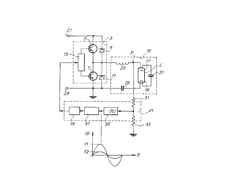
Fig. 1 shows a functional diagram of a circuit
according to the invention,
Figs. 2 and 3 show the waveform of the voltage
signal between the electrodes of the lamp, in case of
defective lamp and in case of lamp absent respectively,
Figs. 4 and 5 show graphs representing the
frequency spectrum of the two signals of Figs. 2 and 3, and
Fig. 6 shows a more detailed constructional
diagram of the circuit diagrammatically indicated in Fig. 1.
Detailed description of the preferred embodiment of the
-, z >o r, t ; ."-,
Represented in Fig. 1, diagrammatically and
limited to the elements relevant in the present description,
is a supply circuit for the discharge lamp L with a supply
inverter. The label 3 generically indicates the supply
inverter, which has two controlled breakers 5 and 7 in a
half-bridge configuration. Diodes
CA 02235355 1998-04-20
_ 6 _
9 and 11 are placed respectively in parallel with the
controlled breakers 5 and 7. The label 13 generically
and diagrammatically indicates the system for
controlling the opening and closing of the breakers 5
and 7, of a type known per se.
Arranged in parallel with the breaker 7 is a
load circuit 15 which comprises, as well as the lamp L
with its electrodes 17 and 19, a capacitor 21 in
parallel with the lamp L and a resonant circuit in
series with the electrodes 17 and 19, which in the
example illustrated is shown diagrammatically with an
inductive component 23 and a capacitive component 25.
The circuit now described is linked via two
contacts 27 and 29 to a rectifier bridge (not
illustrated) which supplies the inverter 3 with a
rectified voltage at a frequency of double the
frequency of the supply network. Via the inverter 3 the
load circuit comprising the discharge lamp L is
supplied with a voltage typically of the order of
10,000-100,000 Hz.
With the ignition of the lamp L, a high voltage
of the order of 1000 V is established between its two
electrodes 17 and 19. This voltage should persist for
an extremely limited interval of time, of the order of
tens of or a few hundred milliseconds, necessary for
the lamp to fire. In case of defective operation of the
lamp, ignition is delayed and the voltage between the
electrodes 17 and 19 persists at the high value of
around 1000 V in the presence of a flow of high current
through a capacitor 21 in parallel with the lamp L.
This entails heavy stressing of the inverter 3 and
hence it is necessary to provide a control circuit
which, depending on the voltage at the point P of the
load circuit, makes provision for disabling the supply
circuit in the case in which the overvoltage condition
persists beyond a preset time threshold.
When the .lamp L is absent from the load
circuit, a high voltage, of the order of 700 V, is
again established at the point P. However, under these
CA 02235355 1998-04-20
_ 7 _
conditions the current through the load circuit is
minimal and corresponds merely to the current through
the stray capacitances of the circuit. Hence, in this
case the supply circuit for the inverter 3 need not be
disabled. The control circuit according to the
invention, which will be described below, makes it
possible to discriminate between these two conditions
of overvoltage on the electrodes of the lamp and hence
makes it possible to turn off the supply in the case of
defective operation only and not in the case of lamp
absent.
Represented in Figs. 2 and 3 is the waveform of
the voltage signal at the point P of the load circuit .
Represented in Fig. 2 is a substantially sinusoidal
waveform with a frequency corresponding to the
frequency f~ of switching of the inverter 3. This is the
waveform of the voltage signal detectable at the point
P in the case of a defect in the operation of the lamp
L. The amplitude of the signal is around 1000 V.
Conversely, in the case of lamp absent, the voltage
signal at the point P takes the profile of Fig. 3 with
an amplitude of around the same order of magnitude as
the previous case (in the example around 700 V), but
with a more complex harmonic content. Figs. 4 and 5
show the frequency spectrum of the two signals . As may
be seen in Fig. 4, the waveform of Fig. 2 is
practically a sinusoidal wave with a frequency f~,
whereas the waveform of Fig. 3, to which the spectrum
of Fig. 5 refers, has a modest harmonic content at the
switching frequency f~ and a large harmonic content at
the higher harmonics.
The control circuit according to the invention
exploits this differing harmonic content of the voltage
signals at the point P under the two conditions of
defective lamp and absent lamp so as to discriminate
the two cases of overvoltage and turn off the supply in
the first case only. With this objective, a voltage
divider 31, 33, at the intermediate point of which is
linked a band-pass filter 35 centred on. the switching
CA 02235355 1998-04-20
_ g _
frequency f~ of the inverter 3, is connected to the
point P of the load circuit.
On account of the different harmonic content of
the voltage signal in the case of defective lamp and of
absent lamp, the output from the filter 35 centred on
the frequency f~ will be a sinusoidal signal of
frequency f~ with a large amplitude in the case of
defective lamp and a very small amplitude in the case
of lamp absent. This is represented qualitatively in
the graph at the bottom of Fig. 1, where time is
plotted along the abcsissa and the output voltage from
the filter 35 along the ordinate and in which the
labels V1 and VZ indicate the amplitudes of the signal
output by the filter respectively in the case of
defective lamp and in the case of absent lamp.
The signal output by the filter 35 is sent to a
level discriminator 37, which dispatches a high signal
to a logic unit 39 when the amplitude of the signal
output by the filter 35 is equal to V1 and a low signal
when the amplitude of the signal output by the filter
35 is equal to V2. The logic unit 39 is therefore able
to discriminate between the two situations of absent
lamp or of defective lamp and depending thereon will
make provision to maintain the inverter 3 under supply
conditions, when the lamp L is absent from the load
circuit, whereas it will make provision to disable the
inverter 3 when the overvoltage at the point P is due
to a defect in the lamp.
Shown in Fig. 6 is a practical embodiment of
the control circuit represented at a functional level
in Fig. 1 and generically labelled 41 therein..
In Fig. 6 elements which are identical to or
correspond to those of Fig. 1 are indicated with .the
same reference numerals and will not be described
again. In this embodiment the band-pass filter 35
consists of an LC cell comprising a capacitor 51 and an
inductor 53 in parallel which form a resonant circuit
at the switching frequency f.~ of the inverter 3. The
filter 35 is linked via a diode 55 to a capacitor 57,
CA 02235355 1998-04-20
_ g _
the latter being charged at the voltage corresponding
to the peak voltage of the signal output by the filter
35. The capacitor 57 is linked to the logic unit 39 via
a Zener diode 59, at the output of which will be
present a low signal when the input voltage is less
than the conduction voltage of the Zener diode and,a
high signal when the input voltage is greater than the
conduction voltage. The conduction voltage of the Zener
diode 59 lies between the values V1 and V2 indicated in
the graph at the bottom of Fig. 1.
In short, the signal at the output of the Zener
diode 59 will be high only in the case of defective
lamp and will remain low in the case of lamp absent or
of normal operation of the load circuit. This signal is
sent to the logic unit 39. which consists of a latch
circuit with two inverting gates 61 and 63 in series
with positive feedback. With this arrangement the
output from the inverting gate 63 will remain at low
level in the case of normal operation or of lamp absent
whereas it will rise to high level and remain steady at
this level, until the operator intervenes on the
circuit, in the case of defective operation of the
lamp. The signal output by the latch circuit is used to
disable the inverter 3.
With the objective of avoiding the intervention
of the protection circuit with each attempted ignition
of the lamp (even under conditions of lamp intact),
there is provided a delay circuit 71 with a delay time
of the order of 100-200 ms. In this way the voltage
peak which occurs for very brief instants at the moment
of ignition of the lamp.,L even when the latter is not
damaged, does not prompt any disabling of the supply
circuit.
To achieve the disabling of the supply inverter
of the lamp L via the signal output by the logic unit
39, this signal can be employed for example to short
circuit the base. of a transistor. This can be the
typical solution for a supply circuit of the self
oscillating type. When the supply to the lamp L is
CA 02235355 1998-04-20
- 10 -
achieved via an integrated control circuit, the signal
generated by the logic unit 39 can be applied to an
enabling/disabling pin of the integrated circuit.
It should be understood that the drawing shows
merely one example given solely as a practical
illustration of the invention, it being possible for
this invention to vary in its forms and arrangements
without however departing from the scope of the concept
underlying the invention. The possible presence of
reference numerals in the enclosed claims has the
objective of facilitating the reading of the claims
with reference to the description and drawing, and does
not limit the scope of the protection represented by
the claims.