Note: Descriptions are shown in the official language in which they were submitted.
CA 02236145 1998-04-29
ARTICLE HAVING A COATING THEREON
Meld of the Invention
This invention relates to multi-layer protective coatings for
articles, particularly brass articles.
Background of the Invent;nr,
It, is currently the practice with various brass articles such
as lamps, trivets, candlesticks, door knobs and handles and the I
like to first buff and polish the surface of the article to a high
gloss and to then apply a protective organic coating, such as one
comprised of acrylics, urethanes, epoxies, and the like, onto this
polished surface. While this system is generally quite
satisfactory it has the drawback that the buffing and polishing
operation, particularly if the article is of a complex shape, is
labor intensive. Also, the known organic coatings are not always
as durable as desired, particularly in outdoor applications where
the articles are exposed to the elements and ultraviolet radiation.
It would, therefore, be quite advantageous if brass articles, or
indeed other metallic articles, could be provided with a coating
which gave the article the appearance of highly polished brass and
also provided wear resistance and corrosion protection. The
present invention provides such a coating.
Summary of the Inven inn
The present invention is directed to a metallic substrate
having a multi-layer coating disposed or deposited on its surface.
More particularly, it is directed to a metallic substrate,
particularly brass, having deposited on its surface multiple
superposed metallic layers of certain specific types of metals or
metal compounds. The coating is decorative and also provides
corrosion and wear resistance. The coating provides the appearance
of highly polished brass, i.e., has a brass color tone. Thus, an
article surface having the coating thereon simulates a highly
polished brass surface.
CA 02236145 1998-04-29
This invention relates to an article comprising a
substrate having disposed on at least a portion of its surface a
multi-layer coating comprising: layer comprised of semi-bright
nickel; layer comprised of bright nickel; layer comprised of
palladium; layer comprised of palladium-nickelalloy; layer
comprised of zirconium or titanium; sandwich layer comprised of
a plurality of alternating layers comprised of zirconium or
titanium and of zirconium compound or titanium compound; and layer
comprised of zirconium or titanium compound.
1 a.
68432-319
CA 02236145 1998-04-29
A first layer deposited directly on the surface of the
substrate is comprised of nickel. The first layer may be
monolithic or it may consist of two different nickel layers such as
a semi-bright nickel layer deposited directly on the surface of the
substrate and a bright nickel layer superimposed over the semi-
bright nickel layer. Disposed over the nickel layer is a layer
comprised of palladium. This palladium layer is thinner than the
nickel layer. Over the palladium layer is a layer comprised of a
palladium alloy, preferably palladium/nickel alloy. Over the
palladium alloy layer is a layer comprised of a non-precious
refractory metal such as zirconium, titanium, hafnium o.r tantalum,
preferably zirconium or titanium. Over the refractory metal layer
is a sandwich layer comprised of a plurality of alternating layers
of non-precious refractory metal, preferably zirconium or titanium,
and non-precious refractory metal compound, preferably a zirconium
compound or titanium compound. A layer comprised of a zirconium
compound, titanium compound, hafnium compound or tantalum compound,
preferably a titanium compound or a zirconium compound such as
zirconium nitride, is disposed over the sandwich layer. A top
layer comprised of the reaction products of a non-precious
refractory metal, preferably zirconium or titanium, oxygen
containing gas, and nitrogen is disposed over the refractory metal
compound layer.
The nickel, palladium and palladium alloy layers are applied
by electroplating. The non-precious refractory metal such as
zirconium, refractory metal compound such as zirconium compound,
and reaction products of non-precious refractory metal, oxygen
containing gas, and nitrogen layers are applied by vapor deposition
processes such as sputter ion deposition.
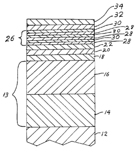
~_r,'-Pf Description of the Drawings
FIG. 1 is a cross-sectional view of a portion of the substrate
having the multi-layer coating deposited on its surface.
2
CA 02236145 2001-O1-22
68432-319
Description of the Preff=:rred Embodiment
The substrate 12 can be any platable metal or
metallic alloy substratf~ such as copper, steel, brass,
tungsten, nickel alloys, and the like. In a preferred
embodiment the substrate is brass.
The nickel layer 13 is deposited on the surface of
the substrate 12 by conventional and well known electroplating
processes. These proce:~ses include using a conventional
electroplating bath sucks as, for example, a Watts bath as the
plating solution. Typically such baths contain nickel sulfate,
nickel chloride, and boric acid dissolved in water. All
chloride, sulfamate and fluoroborate plating solutions can also
be used. These baths can optionally include a number of well
known and conventionally used compounds such as leveling
agents, brighteners, and the like. To produce specularly
bright nickel layer at 7_east one brightener from class I and at
least one brightener from class II is added to the plating
solution. Class I brighteners are organic compounds which
contain sulfur. Class 7..C brighteners are organic compounds
which do not contain su7_fur. Class II brighteners can also
cause leveling and, when added to the plating bath without the
sulfur-containing class I brighteners, result in semi-bright
deposits. These class 7. brighteners include alkyl naphthalene
and benzene sulfonic acids, the benzene and naphthalene di- and
trisulfonic acids, benzene and naphthalene sulfonamides, and
sulfonamides such as saccharin, vinyl and allyl sulfonamides
and sulfonic acids. The class II brighteners generally are
unsaturated organic materials such as, for example, acetylenic
or ethylenic alcohols, ethoxylated and propoxylated acetylenic
alcohols, coumarins and aldehydes. These class I and class II
3
CA 02236145 2001-O1-22
68432-319
brighteners are well known to those skilled in the art and are
readily commercially available. They are described, inter
alia, in U.S. Patent No. 4,421,611.
3a
CA 02236145 1998-04-29
The nickel layer can be a monolithic layer comprised, for
example, of semi-bright nickel or bright nickel, or it can be a
duplex layer containing one layer comprised of semi-bright nickel
and one layer comprised of bright nickel. The thickness of the
nickel layer is generally in the range of from about 100 millionths
(0.000100) of an inch, preferably about 150 millionths (0.000150)
of an inch to about 3,500 millionths (0.0035) of an inch.
As~is well known in the art before the nickel layer is ,
deposited on the substrate the substrate is subjected to said
activation by being placed in a conventional and well known acid
bath.
In a preferred embodiment as illustrated in the Figure, the
nickel layer 13 is actually comprised of two different nickel
layers 14 and 16. Layer 14 is comprised of semi-bright nickel
while layer 16 is comprised of bright nickel. This duplex nickel
deposit provides improved corrosion protection to the underlying
substrate. The semi-bright, sulfur-free plate 14 is deposited by
conventional electroplating processes directly on the surface of
substrate 12. The substrate 12 containing the semi-bright nickel
layer 14 is then placed in a bright nickel plating bath and the
bright nickel layer 16 is deposited on the semi-bright nickel layer
14.
The thickness of the semi-bright nickel layer and the bright
nickel layer is a thickness effective to provide improved corrosion
protection. Generally, the thickness of the semi-bright nickel
layer is at least about 50 millionths (0.00005) of an inch,
preferably at least about 100 millionths (0.000100) of an inch, and
more preferably at least about 150 millionths (0.00015) of an inch.
The upper thickness limit is generally not critical and is governed
by secondary considerations such as cost. Generally, however, a
thickness of about 1,500 millionths (0.0015) of an inch, preferably
about 1,000 millionths (0.001) of an inch, and more preferably
4
CA 02236145 2001-O1-22
68432-319
about 750 millionth (0.00075) of an inch should not be
exceeded. The bright n_~ckel layer 16 generally has a thickness
of at least about 50 mi7_lionths (0.00005) of an inch,
preferably at least about 125 millionths (0.000125) of an inch,
and more preferably at 7_east about 250 millionths (0.000250) of
an inch. The upper thickness range of the bright nickel layer
is not critical and is generally controlled by considerations
such as cost. Generally,. however, a thickness of about 2,500
millionths (0.0025) of an inch, preferably about 2,000
millionths (0.002) of an inch, and more preferably about 1,500
millionths (0.0015) of an inch should not be exceeded. The
bright nickel layer 16 also functions as a leveling layer which
tends to cover or fill in imperfections in the substrate.
Disposed on the bright nickel layer 16 is a
relatively thin layer comprised of palladium. The palladium
strike layer 18 may be deposited on layer 16 by conventional
and well known palladium electroplating techniques. Thus for
example, the anode can be an inert platinized titanium while
the cathode is the substrate 12 having nickel layers 14 and 16
thereon. The palladium is present in the bath as a palladium
salt or complex ion. Some of the complexing agents include
polyamines such as described in U.S. patent No. 4,486,274
incorporated herein by reference. Some other palladium
complexes such as palladium tetra-amine complex used as the
source of palladium in a. number of palladium electroplating
processes are described in U.S. patent Nos. 4,622,110;
4,552,628; and 4,628,165, all of which are incorporated herein
by reference. Some palladium electroplating processes are
described in U.S. patent Nos. 4,487,665; 4,491,507 and
4,545,869.
The palladium strike layer 18 functions, inter alia,
as a primer layer to improve the adhesion of the palladium
alloy, preferably pallad.i.um/nickel alloy layer 20 to the nickel
5
CA 02236145 2001-O1-22
68432-319
layer, such as the bright nickel layer 16 in the embodiment
illustrated in the Figure. This palladium strike layer 18 has
a thickness which is at least effective to improve the adhesion
of the palladium alloy 7_ayer 20 to the nickel layer. The
palladium strike layer generally has a thickness of at least
about 0.25 millionths (0.00000025) of an inch, preferably at
least about 0.5 millionths (0.0000005) of an inch, and more
preferably at least about one millionths (0.000001) of an inch.
Generally, the upper range of thickness is not critical and is
determined by secondary considerations such as cost. However,
the thickness of the palladium strike layer should generally
not exceed about 50 millionths (0.00005) of an inch, preferably
millionths (0.000015) of an inch, and more preferably 10
millionths (0.000010) of: an inch.
15 The palladium alloy, preferably palladium/nickel
alloy layer 20 function;, inter alia, to reduce the galvanic
couple between the refra.c:tory metal such as zirconium,
titanium, hafnium or tantalum containing layers 22 and 24 and
the nickel layer.
The palladium/nickel alloy layer 20 has a weight
ratio of palladium to nickel of from about 50:50 to about 95:5,
preferably from about 60:40 to about 90:10, and more preferably
from about 70:30 to about 85:15.
The palladium/nickel alloy layer may be deposited on
the palladium strike layer 18 by any of the well known and
conventional coating deposition processes including
electroplating. The palladium electroplating processes are
well known to those skilled in the art. Generally, they
include the use of palladium salts or complexes such as
palladious amine chloride salts, nickel salt such as nickel
amine sulfate, organic brighteners, and the like. Some
6
CA 02236145 2001-O1-22
68432-319
illustrative examples of palladium/nickel electroplating
processes and baths are described in U.S. patent Nos.
4,849,303; 4,463,660; 4,416,748; 4,428,820; and 4,699,697.
6a
CA 02236145 1998-04-29
The weight ratio of palladium to nickel in the
palladium/nickel alloy is dependent, inter alia, on the
concentration of palladium (in the form of its salt) and nickel (in
the form of its salt) in the plating bath. The higher the
palladium salt concentration or ratio relative to the nickel salt
concentration in the bath the higher the palladium ratio in the
palladium/nickel alloy.
The thickness of the palladium/nickel alloy layer 20 is a
thickness which is at least effective to reduce the galvanic
coupling between the hafnium, tantalum, zirconium or titanium,
preferably zirconium or titanium, and more preferably zirconium
containing layers and nickel layer 16. Generally, this thickness
is at least about 2 millionths (0.000002) of an inch, preferably at
least about 5 millionths (0.000005) of an inch, and more preferably
at least about 10 millionths (0.00001) of an inch. The upper
thickness range is not critical and is generally dependent on
economic considerations. Generally, a thickness of about 100
millionths (0.0001) of an inch, preferably about 70 millionths
(0.00007), and more preferably about 60 millionths (0.00006) of an
inch should not be exceeded.
Disposed over the palladium alloy, preferably palladium/nickel
alloy layer 20 is a layer 22 comprised of a non-precious refractory
metal such as hafnium, tantalum, zirconium or titanium, preferably
zirconium or titanium, and more preferably zirconium.
Layer 22 is deposited on layer 20 by conventional and well
known techniques such as vacuum coating, physical vapor deposition
such as ion sputtering, and the like. Ion sputtering techniques
and equipment are disclosed, inter alia, in T. Van Vorous, "Planar
Magnetron Sputtering; A New Industrial Coating Technique", Solid
State Technology, Dec. 1976, pp 62-66; U. Kapacz and S. Schulz,
"Industrial Application of Decorative Coatings - Principle and
Advantages of the Sputter Ion Plating Process", Soc. Vac. Coat.,
CA 02236145 2001-O1-22
68432-319
Proc. 34th Arn. Tech. Co:nf., Philadelphia, U.S.A., 1991, 48-61;
and U.S. patent Nos. 4,7_62,954 and 4,591,418.
Briefly, in the sputter ion deposition process the
refractory metal such a:~ titanium or zirconium target, which is
the cathode, and the substrate are placed in a vacuum chamber.
The air in the chamber i_~~ evacuated to produce vacuum
conditions in the chamber. An inert gas, such as Argon, is
introduced into the chamber. The gas particles are ionized and
are accelerated to the target to dislodge titanium or zirconium
atoms. The dislodged target material is then typically
deposited as a coating film on the substrate.
Layer 22 generally has a thickness of at least about
0.25 millionths (0.00000025) of an inch, preferably at least
about 0.5 millionths (0.0000005) of an inch, and more
preferably at least about one millionth (0.000001) of an inch.
The upper thickness range is not critical and is generally
dependent upon considera.t:ions such as cost. Generally,
however, layer 22 should not be thicker than about 50
millionths (0.00005) of an inch, preferably about 15 millionths
(0.000015) of an inch, a.nd more preferably about 10 millionths
(0.000010) of an inch.
In a preferrea. embodiment of the present invention
layer 22 is comprised of titanium or zirconium, preferably
zirconium, and is deposited by sputter ion plating.
Disposed over layer 22 is a sandwich layer 26
comprised of alternating layers 28 and 30 of a non-precious
refractory metal compound and a non-precious refractory metal.
Layer 26 generally has a thickness of from about 50
millionths (0.00005) of_ an inch to about one millionth
8
CA 02236145 2001-O1-22
68432-319
(0.000001) of an inch, preferably from about 40 millionths
(0.00004) of an inch to about two millionths (0.000002) of an
inch, and more preferably from
8a
CA 02236145 1998-04-29
about 30 millionths (0.00003) of an inch to about three millionths
(0.000003) of an inch.
The non-precious refractory metal compounds comprising layers
28 include a hafnium compound, a tantalum compound, a titanium
compound or a zirconium compound, preferably a titanium compound or
a zirconium compound, and more preferably a zirconium compound.
These compounds are selected from nitrides, carbides and
carbonitrides, with the nitrides being preferred. Thus, the .
titanium compound is selected from titanium nitride, titanium
carbide and titanium carbonitride, with titanium nitride being
preferred. The zirconium compound is selected from zirconium
nitride, zirconium carbide and zirconium carbonitride, with
zirconium nitride being preferred.
The nitride compounds are deposited by any of the conventional
and well known reactive vacuum deposition processes including
reactive ion sputtering. Reactive ion sputtering is generally
similar to ion sputtering except that a gaseous material which
reacts with the dislodged target material is introduced into the
chamber. Thus, in the case where zirconium nitride comprises
layers 28, the target is comprised of zirconium and nitrogen gas is
the gaseous material introduced into the chamber.
Layers 28 generally have a thickness of at least about two
hundredths of a millionth (0.00000002) of an inch, preferably at
least about one tenth of a millionth (0.0000001) of an inch, and
more preferably at least about five tenths of a millionth
(0.0000005) of an inch. Generally, the layers 28 should not be
thicker than about 25 millionths (0.000025) of an inch, preferably
about 10 millionths (0.000010) of an inch, and more preferably
about five millionths (0.000005) of an inch.
The layers 30 alternating in the sandwich layer 26 with the
non-precious refractory metal compound layers 28 are comprised of
a non-precious refractory metal such as described for layer 22.
9
CA 02236145 1998-04-29
The preferred metals comprising layers 30 are titanium and
zirconium.
Layers 30 are deposited by any of the conventional and well
known vapor deposition processes such as sputter ion deposition or
plating processes.
Layers 30 have a thickness of at least about two hundredths of
a millionth (0.00000002) of an inch, preferably at least about one
tenth of a millionth (0.0000001) of an inch, and more preferably at -
least about five tenths of a millionth (0.0000005) of an inch.
Generally, layers 30 should not be thicker than about 25 millionths
(0.000025) of an inch, preferably about 10 millionths (0.000010) of
an inch, and more preferably about five millionths (0.000005) of an
inch.
The number of alternating layers of metal 30 and metal nitride
28 in sandwich layer 26 is generally an amount effective to reduce
stress and improve chemical resistance. Generally this amount is
from about 50 to about two, preferably from about 40 to about four
layers 28, 30, and more preferably from about 30 to about six
layers 28, 30.
The sandwich layer 26 comprised of multiple alternating layers
28 and 30 generally serves to, inter alia, reduce film stress,
increase overall film hardness, improve chemical resistance, and
realign the lattice to reduce pores and grain boundaries from
extending through the entire film.
A preferred method of forming the sandwich layer 26 is by
utilizing ion sputter plating to deposit a layer 30 of non-precious
refractory metal such as zirconium or titanium followed by reactive
ion sputter plating to deposit a layer 28 of non-precious
refractory metal nitride such as zirconium nitride or titanium
nitride.
Preferably the flow rate of nitrogen gas is varied (pulsed)
during the ion sputter plating between zero (no nitrogen gas is
CA 02236145 1998-04-29
introduced) to the introduction of nitrogen at a desired value to
form multiple alternating layers 28, 30 of metal 30 and metal
nitride 28 in the sandwich layer 26.
The thickness proportionment of layers 30 to 28 is at least
about 20/80, preferably 30/70, and more preferably 40/60.
Generally, it should not be above about 80/20, preferably 70/30,
and more preferably 60/40.
Disposed over the sandwich layer 26 is a layer 32 comprised of
a non-precious refractory metal compound, preferably a non-precious
refractory metal nitride, carbonitride, or carbide, and more
preferably a nitride.
Layer 32 is comprised of a hafnium compound, a tantalum
compound, a titanium compound or a zirconium compound, preferably
a titanium compound or a zirconium compound, and more preferably a
zirconium compound. The titanium compound is selected from
titanium nitride, titanium carbide, and titanium carbonitride, with
titanium nitride being preferred. The zirconium compound is
selected from zirconium nitride, zirconium carbonitride, and
zirconium carbide, with zirconium nitride being preferred.
Layer 32 provides wear and abrasion resistance and the desired
color or appearance, such as for example, polished brass. Layer 32
is deposited on layer 26 by way of the well known and conventional
plating or deposition processes such as vacuum coating, reactive
sputter ion plating, and the like. The preferred method is
reactive ion sputter plating.
Layer 32 has a thickness at least effective to provide
abrasion resistance. Generally, this thickness is at least 2
millionths (0.000002) of an inch, preferably at least 4 millionths
(0.000004) of an inch, and more preferably at least 6 millionths
(0.000006) of an inch. The upper thickness range is generally not
critical and is dependent upon considerations such as cost.
Generally a thickness of about 30 millionths (0.00003) of an inch,
11
CA 02236145 1998-04-29
preferably about 25 millionths (0.000025) of an inch, and more
preferably about 20 millionths (0.000020) of an inch should not be
exceeded.
Zirconium nitride is the preferred coating material as it most
closely provides the appearance of polished brass. By controlling
the amount of nitrogen gas introduced into the reaction vessel
during reactive ion sputtering the. color of the zirconium nitride
can be made similar to that of brass of various hues.
In one embodiment of the invention a layer 34 comprised of the
reaction products of a non-precious refractory metal, an oxygen
containing gas such as oxygen, and nitrogen is deposited onto the
layer 32. The metals that may be employed in the practice of this
invention are those which are capable of forming both a metal oxide
and a metal nitride under suitable conditions, for example, using
reactive gases comprised of oxygen and nitrogen. The metals may
be, for example, tantalum, hafnium, zirconium and titanium,
preferably titanium and zirconium, and more preferably zirconium.
The reaction products of the metal, oxygen and nitrogen are
generally comprised of the metal oxide, metal nitride and metal
oxy-nitride. Thus, for example, the reaction products of
zirconium, oxygen and nitrogen generally comprise zirconium oxide,
zirconium nitride and zirconium oxy-nitride.
The layer 34 can be deposited by a well known and conventional
deposition technique, including reactive sputtering of a pure metal
target or a composite target of oxides, nitrides and/or metals,
reactive evaporation, ion and ion assisted sputtering, ion plating,
molecular beam epitaxy, chemical vapor deposition and deposition
from organic precursors in the form of liquids. Preferably,
however, the metal reaction products of this invention are
deposited by reactive ion sputtering. In a preferred embodiment
reactive ion sputtering is used with oxygen and nitrogen being
introduced simultaneously.
12
CA 02236145 2001-O1-22
68432-319
These metal oxides, metal oxy-nitrides and metal
nitrides including zircc>nium oxide and zirconium nitride alloys
and their preparation arid deposition are conventional and well
known and are disclosed, inter alia, in U.S. patent No.
5,367,285.
In another emu>odiment instead of layer 34 being
comprised of the reaction products of a refractory metal,
oxygen and nitrogen it i~> comprised of non-precious refractory
metal oxide. The refractory metal oxides of which layer 34 is
comprised include, but a.re not limited to, hafnium oxide,
tantalum oxide, zirconium oxide and titanium oxide, preferably
titanium oxide and zirconium oxide, and more preferably
zirconium oxide. These oxides and their preparation are
conventional and well known.
The metal, oxygen and nitrogen reaction products or
metal oxide containing layer 34 generally has a thickness at
least effective to provide improved acid resistance. Generally
this thickness is at least five hundredths of a millionth
(0.00000005) of an inch, preferably at least about one tenth of
a millionth (0.0000001) of an inch, and more preferably at
least about 0.15 of a millionth (0.00000015) of an inch.
Generally, layer 34 should not be thicker than about five
millionths (0.000005) of an inch, preferably about two
millionths (0.000002) of an inch, and more preferably about one
millionth (0.000001) of an inch.
In order that the invention may be more readily
understood the following example is provided. The example is
illustrative and does not limit the invention thereto.
rwTnrtnr n ~
Brass door escutcheons are placed in a conventional
13
CA 02236145 2001-O1-22
68432-319
soak cleaner bath containing the standard and well known soaps,
detergents, defloculants .and the like which is maintained at a
pH of 8.9 - 9.2 and a temperature of 180 - 200°F for 30
minutes. The brass escutcheons are then placed for six minutes
in a conventional
13a
CA 02236145 1998-04-29
ultrasonic alkaline cleaner bath. The ultrasonic cleaner bath has
a pH of 8.9 - 9.2, is maintained at a temperature of about 160 -
180oF, and contains the conventional and well known soaps,
detergents, defloculants and the like. After the ultrasonic
cleaning the escutcheons are rinsed and placed in a conventional
alkaline electro cleaner bath for about two minutes. The electro
cleaner bath contains an insoluble submerged steel anode, is
maintained at a temperature of about 140 - 180oF, a pH of about
10.5 - 11.5, and contains standard and conventional detergents.
The escutcheons are then rinsed twice and placed in a conventional
acid activator bath for about one minute. The acid activator bath
has a pH of about 2.0 - 3.0, is at an ambient temperature, and
contains a sodium fluoride based acid salt. The escutcheons are
then rinsed twice and placed in a semi-bright nickel plating bath
for about 10 minutes. The semi-bright nickel bath is a
conventional and well known bath which has a pH of about 4.2 - 4.6,
is maintained at a temperature of about 130 - 150~F, contains NiS04,
NiCLz, boric acid, and brighteners. A semi-bright nickel layer of
an average thickness of about 250 millionths of an inch (0.00025)
is deposited on the surface of the escutcheon.
The escutcheons containing the layer of semi-bright nickel are
then rinsed twice and placed in a bright nickel plating bath for
about 24 minutes. The bright nickel bath is generally a
conventional bath which is maintained at a temperature of about 130
- 150~F, a pH of about 4.0 - 4.8, contains NiS04, NiCLz, boric acid,
and brighteners. A bright nickel layer of an average thickness of
about 750 millionths (0.00075) of an inch is deposited on the semi-
bright nickel layer. The semi-bright and bright nickel plated
escutcheons are rinsed three times and placed for about one and a
half minutes in a conventional palladium plating bath. The
palladium bath utilizes an insoluble platinized niobium anode, is
maintained at a temperature of about 95 - 140oF, a pH of about 3.7
- 4.5, contains from about 1-5 grams per liter of palladium (as
metal), and about 50-100 grams per liter of sodium chloride. A
palladium layer of an average thickness of about three millionths
14
CA 02236145 1998-04-29
(0.000003) of an inch is deposited on the bright nickel layer. The
palladium plated escutcheons are then rinsed twice.
After rinsing the palladium coated escutcheons are placed for
about four minutes in a conventional palladium/nickel plating bath.
The palladium nickel plating bath is at a temperature of about 85 -
100oF, a pH of about 7.8 - 8.5, and utilizes an insoluble
platinized niobium anode. The bath contains about 6 - 8 grams per
liter of palladium (as metal), 2-4 grams per liter of nickel (as
metal), NH4 C1, wetting agents and brighteners. A palladium/nickel
alloy (about 80 weight percent of palladium and 20 weight percent
of nickel) having an average thickness of about 37 millionths
(0.000037) of an inch is deposited on the palladium layer. After
the palladium/nickel layer is deposited the escutcheons are
subjected to five rinses, including an ultrasonic rinse, and are
dried with hot air.
The palladium/nickel plated escutcheons are placed in a
sputter ion plating vessel. This vessel is a stainless steel
vacuum vessel marketed by Leybold A.G. of Germany. The vessel is
generally a cylindrical enclosure containing a vacuum chamber which
is adapted to be evacuated by means of pumps. A source of argon
gas is connected to the chamber by an adjustable valve for varying
the rate of flow of argon into the chamber. In addition, two
sources of nitrogen gas are connected to the chamber by an
adjustable valve for varying the rate of flow of nitrogen into the
chamber.
Two pairs of magnetron-type target assemblies are mounted in
a spaced apart relationship in the chamber and connected to
negative outputs of variable D.C. power supplies. The targets
constitute cathodes and the chamber wall is an anode common to the
target cathodes. The target material comprises zirconium.
A substrate carrier which carries the substrates, i.e.,
escutcheons, is provided, e.g., it may be suspended from the top of
the chamber, and is rotated by a variable speed motor to carry the
substrates between each pair of magnetron target assemblies. The
CA 02236145 1998-04-29
carrier is conductive and is electrically connected to the negative
output of a variable D.C. power supply.
The plated escutcheons are mounted onto the substrate carrier
in the sputter ion plating vessel. The vacuum chamber is evacuated
to a pressure of about SxlO-3 millibar and is heated to about 400~C
via a radiative electric resistance heater. The target material is
sputter cleaned to remove contaminants from its surface. Sputter
cleaning is carried out for about one half minute by applying power
to the cathodes sufficient to achieve a current flow of about 18 '
amps and introducing argon gas at the rate of about 200 standard
cubic centimeters per minute. A pressure of about 3x10-' millibars
is maintained during sputter cleaning.
The escutcheons are then cleaned by a low pressure etch
process. The low pressure etch process is carried on for about
five minutes and involves applying a negative D.C. potential which
increases over a one minute period from about 1200 to about 1400
volts to the escutcheons and applying D.C. power to the cathodes to
achieve a current flow of about 3.6 amps. Argon gas is introduced
at a rate which increases over a one minute period from about 800
to about 1000 standard cubic centimeters per minute, and the
pressure is maintained at about 1.1x10⁻² millibars. The escutcheons
are rotated between the magnetron target assemblies at a rate of
one revolution per minute. The escutcheons are then subjected to
a high pressure etch cleaning process for about 15 minutes. In the
high pressure etch process argon gas is introduced into the vacuum
chamber at a rate which increases over a 10 minute period from
about 500 to 650 standard cubic centimeters per minute (i.e., at
the beginning the flow rate is 500 sccm and after ten minutes the
flow rate is 650 sccm and remains 650 sccm during the remainder of
the high pressure etch process), the pressure is maintained at
about 2x10⁻¹ millibars, and a negative potential which increases
over a ten minute period from about 1400 to 2000 volts is applied
to the escutcheons. The escutcheons are rotated between the
magnetron target assemblies at about one revolution per minute.
The pressure in the vessel is maintained at about 2x10⁻¹ millibar.
16
CA 02236145 1998-04-29
The escutcheons are then subjected to another low pressure
etch cleaning process for about five minutes. During this low
pressure etch cleaning process a negative potential of about 1400
volts is applied to the escutcheons, D.C. power is applied to the
cathodes to achieve a current flow of about 2.6 amps, and argon gas
is introduced into the vacuum chamber at a rate which increases
over a five minute period from about 800 sccm (standard. cubic
centimeters per minute) to about 1000 sccm. The pressure is
maintained at about 1.1x10⁻² millibar and the escutcheons are '
rotated at about one rpm.
The target material is again sputter cleaned for about one
minute by applying power to the cathodes sufficient to achieve a
current flow of about 18 amps, introducing argon gas at a rate of
about 150 sccm, and maintaining a pressure of about 3x10'3
millibars.
During the cleaning process shields are interposed between the
escutcheons and the magnetron target assemblies to prevent
deposition of the target material onto the escutcheons.
The shields are removed and a layer of zirconium having an
average thickness of about three millionths (0.000003) of an inch
is deposited on the palladium/nickel layer of the escutcheons
during a four minute period. This sputter deposition process
comprises applying D.C. power to the cathodes to achieve a current
flow of about 18 amps, introducing argon gas into the vessel at
about 450 sccm, maintaining the pressure in the vessel at about
6x10-' millibar, and rotating the escutcheons at about 0.7
revolutions per minute.
After the zirconium layer is deposited the sandwich layer of
alternating zirconium nitride and zirconium layers is deposited
onto the zirconium layer. Argon gas is introduced into the vacuum
chamber at a rate of about 250 sccm. D.C. power is supplied to the
cathodes to achieve a current flow of about 18 amps. A bias
voltage of about 200 volts is applied to the substrates. Nitrogen
gas is introduced at an initial rate of about 80 sccm. The flow of
nitrogen is then reduced to zero or near zero. This pulsing of
17
CA 02236145 1998-04-29
nitrogen is set to occur at about a 50% duty cycle. The pulsing
continues for about 10 minutes resulting in a sandwich stack with
about six layers of an average thickness of about one millionth
(0.000001) of an inch each. The sandwich stack has an average
thickness of about six millionths (0.000006) of an inch.
After the sandwich layer of alternating layers of zirconium
nitride and zirconium ,a layer of zirconium nitride having an
average thickness of about 10 millionths (0.00001) of an inch is
deposited on the sandwich stack during a period of about 20
minutes. In this step the nitrogen is regulated to maintain a
partial ion current of about 6.3 x 10⁻¹¹ amps. The argon, do
power, and bias voltage are maintained as above.
Upon completion of the deposition of the zirconium nitride
layer, a thin layer of the reaction products of zirconium, oxygen
and nitrogen is deposited having an average thickness of about 0.25
millionths (0.00000025) of an inch during a period of about 30
seconds. In this step the introduction of argon is kept at about
250 sccm, the cathode current is kept at about 18 amps, the bias
voltage is kept at about 200 volts and the nitrogen flow is set at
about 80 sccm. Oxygen is introduced at a rate of about 20 sccm.
While certain embodiments of the invention have been described
for purposes of illustration, it is to be understood that there may
be various embodiments and modifications within the general scope
of the invention.
18