Note: Descriptions are shown in the official language in which they were submitted.
CA 02236287 2001-06-27
- 1 -
BACKGROUND OF THE INVENTION
FIELD OF THE INVENTION
The present invention relates to a code division
multiple access (CDMA) receiver used for a digital portable
telephone or the like, or more in particular to a synchro-
nization tracking circuit of a CDMA receiver.
DESCRIPTION OF THE RELATED ART
A conventional- CDMA receiver of this type is
disclosed in JP-A-9--18446 published June 1997, for example.
In the conventional CDMA receiver, as shown in
Fig. 1, an analog reception signal is over-sampled and
converted into a digital reception signal by an A/D
converter 610. A correlator 620 obtains a correlation
value between the digital reception signal and a spreading
code of a pilot channel (pilot spreading code) in accord-
once with a reception timing of the receiver. In the
process, a reception timing correlator 621 obtains a
correlation value bEatween the digital reception signal and
the pilot spreading code which is synchronous with a
present reception timing. An early timing correlator 622
obtains a correlation value between the digital reception
signal and the pilot: spreading code which is synchronous
with an early reception timing having a phase ahead of the
present reception timing. A late timing correlator 623
obtains a correlation value between the digital reception
CA 02236287 1998-04-29
- 2 -
signal and the pilot spreading code which is synchronous
with a late reception timing signal having a phase lagging
behind the present reception timing.
A phase difference detecting unit 630 obtains a
phase difference between the reception signal and the
present reception timing based on the three correlation
values obtained by the correlator 620. A timing control-
ling unit 640 synchronizes the reception timing, which is
used for obtaining the correlation values in the correlator
620, with the reception signal by shifting the reception
timing in such a direction as to eliminate the phase
difference obtained by the phase difference detecting unit
630. In the case where the reception timing is shifted
intentionally, the direction of the phase difference to be
shifted and the angle to be shifted are indicated to the
timing controlling unit 640.
With the above-mentioned conventional CDMA
receiver, the system configuration is restricted for
selection of the sampling frequency of the A/D converter
610. Nevertheless, any sampling frequency can be selected.
An arbitrary selection of the sampling frequency,
however, makes it necessary to perform a dividing operation
for calculating, setting and implementing a correction
value of the reception timing when the phase difference
between the reception signal and the reception timing is
detected to correct the reception timing. The result is
longer time required for calculating the correction value
of the reception timing.
CA 02236287 2001-06-27
- 3 -
SUMMARY OF THE INVENTION
An object of the present invention is to provide a CDMA
receiver capable of shortening the time required for
calculating a correctian value of a reception timing.
According to a first: aspect of the present invention,
there is provided a CDMA receiver which comprises: an A/D
converter for over-sampling an analog reception baseband
signal with a sampling clock having a frequency 2n times
higher than that of a chip clock and for converting the
analog reception baseband signal into a digital reception
basband signal; a correlator for obtaining a correlation
value between the digital reception baseband signal and a
pilot spreading code which is synchronous with a reception
timing; a phase difference detecting unit for obtaining a
phase difference between the digital reception baseband
signal and the reception timing based on the correlation
value; and a timing controlling unit for changing the
reception timing so as to eliminate the phase difference.
The timing controlling unit includes a chip phase shifting
unit for changing the reception timing in chips and 1/2n-chip
phase shifting unit for changing the reception timing in 1/2n
chips.
According to a further aspect of the present invention,
there is provided a CDMA receiver, wherein the timing
controlling is constituted using a synchronizing
CA 02236287 1998-04-29
- 4 -
circuit.
BRIEF DESCRIPTION OF THE DRAWINGS
Fig. 1 is a block diagram showing a configuration
of a conventional CDMA receiver.
Fig. 2 is a block diagram showing a configuration
of a CDMA receiver according to a first embodiment of the
present invention.
Fig. 3 is a timing chart for explaining the
operation of the CDMA receiver shown in Fig. 2.
Fig. 4 is a block diagram showing a configuration
of a CDMA receiver according to a second embodiment of the
present invention.
Fig. 5 is a block diagram showing a configuration
of a CDMA receiver according to a third embodiment of the
present invention.
Fig. 6A is a diagram showing an example of an
output signal of a 1/2n-chip phase shifting unit in the CDMA
receiver of Fig. 5.
Fig. 6B is a diagram showing an example of an
output signal of a chip phase shifting unit in the CDMA
receiver of Fig. 5.
DESCRIPTION OF THE PREFERRED EMBODIMENTS
(First Embodiment)
In a CDMA receiver according to a first embodi-
ment of the present invention, a frequency of a sampling
clock of an A/D converter is set to a value 2n times higher
CA 02236287 1998-04-29
- 5 -
than that of a chip clock. As shown in Fig. 2, the CDMA
receiver according to this embodiment comprises an A/D
converter 10; a correlator 20 which includes a reception
timing correlator 21, an early timing correlator 22 and a
late timing correlator 23; a phase difference detecting
unit 30; and a timing controlling unit 40.
In the A/D converter 10, an analog reception
baseband signal obtained by frequency change and orthogonal
detection of a reception high-frequency signal in a RF
section (not shown) is over-sampled with the sampling clock
the frequency of which is 23 (= 8) times higher than that of
the chip clock, and is converted into a digital reception
baseband signal.
Each of the reception timing correlator 21, the
early timing correlator 22 and the late timing correlator
23 of the correlator 20 is a circuit for obtaining a
correlation value between the digital reception baseb~nd
signal and a pilot spreading code (a spreading code used
for a pilot channel), and comprises a pilot spreading code
generator, a complex correlator and a symbol integrator.
The operation timings of these correlators are controlled
by the timing controlling unit 40. The reception timing
correlator 21 obtains a correlation value between the
digital reception baseband signal and the pilot spreading
code which is synchronous with the present reception
timing. The early timing correlator 22 obtains a correla-
tion value between the digital reception baseband signal
and the pilot spreading code which is synchronous with an
CA 02236287 1998-04-29
- 6 -
early reception timing having a phase ahead of the present
reception timing. The late timing correlator 23 obtains a
correlation value between the digital reception baseband
signal and the pilot spreading code which is synchronous
with a late reception timing having a phase lagging behind
the present reception timing.
The phase difference detecting unit 30 obtains a
phase difference between the digital reception baseband
signal and the present reception timing based on the three
correlation values outputted from the correlator 20, judges
whether the present reception timing is coincident with the
digital reception baseband signal, and in the case where it
is not coincident, indicates a control amount for correct-
ing the reception timing to the timing controlling unit 40.
Also, in the case where the reception timing is to be
shifted intentionally, the amount of the intended shift is
indicated from the phase difference detecting unit 30 to
the timing controlling unit 40. The timing controlling
unit 40 shifts the reception timing of the receiver in
compliance with the indication from the phase difference
detecting unit 30.
The operation of the CDMA receiver according to
this embodiment will be described with reference to Fig. 3.
The analog reception baseband signal is over-sampled with
the sampling clock the frequency of which is 23 (= 8) times
higher than that of the chip clock (refer to a chip clock
timing and a over-sampled value in Fig. 3), and is
converted into the digital reception baseband signal by the
CA 02236287 1998-04-29
_ 7 _
A/D converter 10. Assuming that the present reception
timing (the reception timing presently indicated by the
timing controlling unit 40 to the correlator 20) is given
as a reception timing to shown in Fig. 3, the reception
timing correlator 21 obtains the correlation value between
the digital reception baseband signal and the pilot spread-
ing code which is synchronous with the reception timing ta.
The early timing correlator 2 obtains the correlation value
between the digital reception baseband signal and the pilot
spreading code which is synchronous with an early reception
timing tx having a phase ahead of the reception timing ta.
Further, the late timing correlator 23 obtains the correla-
tion value between the digital reception baseband signal
and the pilot spreading code which is synchronous with a
late reception timing ty having a phase lagging behind the
reception timing ta. The phase difference detecting unit
30 detects the phase difference between the digital
reception baseband signal and the present reception timing
based on the three correlation values thus obtained. The
timing controlling unit 40 shifts the reception timing in
such a direction as to eliminate the phase difference
detected in the phase difference detecting unit 30.
For shifting the reception timing by about two
samples forward (in x direction), for example, the
direction and the control amount of two samples are
indicated from the phase difference detecting unit 30 to
the timing controlling unit 40. In the process, if the
reception timing is intentionally shifted backward (in y
CA 02236287 1998-04-29
- g -
direction) by three chips and one sample (one chip equals 8
samples), this shift amount (three chips and one sample) is
added to the control amount (two samples), and is indicated
from the phase difference detecting unit 30 to the timing
controlling unit 40. The amount by which the reception
timing is to be shifted is given as (-2 samples) + (3 chips
+ 1 sample) - 2 chips + 7 samples. Thus, the reception
timing is shifted by 2 chips + 7 samples backward. Since
the frequency of the sampling clock of the A/D converter 10
is 23 (= 8) times higher than that of chip clock, the amount
by which the reception timing is shifted is calculated by
the modulo-8 arithmetic operation which imposes no load on
the hardware/software processing.
Another advantage is that since one chip is equal
to 8 (= 23) samples, a similar management is possible simply
by using the carry from three bits in a sampling period
unit, regardless of whether the reception timing is managed
by the phase difference detecting unit 30 in a sampling
period unit alone or in a sampling period plus chip unit.
The timing controlling unit 40 obtains the amount
by which the reception timing is shifted, in accordance
with the control amount and the shift amount indicated from
the phase difference detecting unit 30. The correlator 20
shifts the reception timing by the amount obtained by the
timing controlling unit 40, and thus obtains three correla-
tion values as described above.
As explained above, with the CDMA receiver
according to this embodiment, the phase difference
CA 02236287 1998-04-29
- 9 -
detecting unit 30 and the timing controlling unit 40 can be
configured of arithmetic processing means in simple hard-
ware or software of modulo-2n by setting the frequency of
the sampling clock of the A/D converter to the value 2n
times as high as that of the chip clock.
(Second Embodiment)
In a CDMA receiver according to a second embodi-
ment of the present invention, a frequency of a sampling
clock of an A/D converter is set to a value 2° times as high
as that of a chip clock, and a phase shifting unit in chips
and a phase shifting unit in 1/2n chips (hereinafter
referred to as a chip phase shifting unit and a 1/2n-chip
phase shifting unit, respectively) are provided in a timing
controlling unit. Specifically, the CDMA receiver accord-
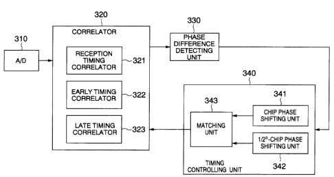
ing to this embodiment, as shown in Fig. 4, comprises an
A/D converter 310; a correlator 320 including a reception
timing correlator 321, an early timing correlator 322 and a
late timing correlator 323; a phase difference detecting
unit 330; and a timing controlling unit 340 including a
chip phase shifting unit 341, a 1/2n-chip phase shifting
unit 343 and a matching unit 343. The chip phase shifting
unit 341 is for changing the reception timing in chips, and
the 1/2n-chip phase shifting unit 342 is for changing the
reception timing in sampling timings of the A/D converter
310. The matching unit 343 is for combining the reception
timing changed by the chip phase shifting unit 341 with the
reception timing changed by the 1/2n-chip phase shifting
unit 342.
CA 02236287 1998-04-29
- 10 -
The operations of the A/D converter 310, the
correlator 320 and the phase difference detector 330 of the
CDMA receiver according to this embodiment are similar to
those of the A/D converter 10, the correlator 20 and the
phase difference detector 30 of the CDMA receiver according
to the first embodiment shown in Fig. 2. Therefore, only
the operation of the timing controlling unit 340 will be
explained in detail below.
A phase shift amount indication data outputted
from the phase difference detecting unit 330 to the timing
controlling unit 340 indicates a phase shift amount in
sampling timings of the A/D converter 310. Assuming that
the frequency of the sampling clock of the A/D converter
310 is 23 (= 8) times as high as that of the chip clock and
the amount of the phase shifted for the time of three chips
(= 3 X 8 = 24 sampling clocks) is indicated by the phase
shift amount indication data, the phase shift amount
indication data has a total of 5 bits. In the phase shift
amount indication data, the two high-order bits indicates a
phase shift amount in chips, and the three low-order bits
indicates a phase shift amount in sampling timings of the
A/D converter 310.
In the case where the two high-order bits of the
phase shift amount indication data are "00", for example,
the reception timing is not changed by the chip phase
shifting unit 341. In the case where the two high-order
bits of the phase shift amount indication data are "O1", in
contrast, the reception timing is changed by one chip,
CA 02236287 1998-04-29
- 11 -
while in the case where the two high-order bits of the
phase shift amount indication data are "10", the reception
timing is changed by two chips by the chip phase shifting
unit 341. In the case where the three low-order bits of
the phase shift indication data are "000", for example, the
reception timing is not changed by the 1/2°-chip phase
shifting unit 342. In the case where the three low-order
bits of the phase shift amount indication data are "001",
the reception timing is changed by 1/23 (= 1/8) chips, while
in the case where the three low-order bits of the phase
shift amount indication data are "011", the reception
timing is changed by 3/23 (= 3/8) chips by the 1/2n-chip
phase shifting unit 342. The matching unit 343 combines
the reception timing changed by the chip phase shifting
unit 341 with the reception timing changed by the 1/2n-chip
phase shifting unit 342 thereby to change the reception
timing in accordance with the phase shift amount indication
data supplied from the phase difference detecting unit 330.
In the case where the phase shift amount indication data
are "01011", for example, the reception timing changed by
one chip in the chip phase shifting unit 341 and the
reception timing changed by 3/8 chips in the 1/2°-chip phase
shifting unit 342 are combined with each other by the
matching unit 343, thereby producing the reception timing
changed by (1 + 3/8) chips. The direction in which the
phase of the reception timing is shifted is also indicated
by the phase difference detecting unit 330 to the timing
controlling unit 340.
CA 02236287 1998-04-29
- 12 -
As described above, in the CDMA receiver accord-
ing to this embodiment, the timing controlling unit 340
includes the chip phase shifting unit 341, the 1/2n-chip
phase shifting unit 342 and the matching unit 343. There-
fore, the phase shift amount can be indicated from the
phase difference detecting unit 330 to the timing control-
ling unit 340 in sampling timings of the A/D converter 310
(i.e. in 1/2n chips).
(Third Embodiment)
In a CDMA receiver according to a third embodi-
ment of the present invention, a frequency of a sampling
clock of an A/D converter is set to 2n times as high as that
of a chip clock and a timing controlling unit including a
chip phase shifting unit, a 1/2n-chip phase shifting unit
and a matching unit is constituted using synchronizing
circuits Specifically, the CDMA receiver according to this
embodiment comprises, as shown in Fig. 5, an A/D converter
410; a correlator 420 including a reception timing
correlator 421, an early timing correlator 422 and a late
timing correlator 432; a phase difference detecting unit
430; and a timing controlling unit 440 including a chip
phase shifting unit 441, a 1/2°-chip phase shifting unit 442
and a matching unit 443. The chip phase shifting unit 441
is for changing the reception timing in chips and outputs a
clock 444. The 1/2n-chip phase shifting unit 442 is for
changing the reception timing in sampling timings of the
A/D converter 410 and outputs a clock 445. The matching
unit 443 combines the reception timing changed by the chip
CA 02236287 1998-04-29
- 13 -
phase shifting unit 441 and the reception timing changed by
the 1/2n-chip phase shifting unit 442 based on the clocks
444 and 445. The clock 446 outputted from the matching
unit 443 functions as an enable signal for a synchronizing-
system circuit activated in synchronism with the sampling
clock of the A/D converter 410.
The operations of the A/D converter 410, the
correlator 420 and the phase difference detecting unit 430
of the CDMA receiver according to this embodiment are
similar to those of the A/D converter 10, the correlator 20
and the phase difference detecting unit 30 of the CDMA
receiver according to the first embodiment. Therefore,
only the operation of the timing controlling unit 440 will
be described in detail below with reference to Figs. 6A and
6B.
When a phase shift amount data is outputted from
the phase difference detecting unit 430 to the timing
controlling unit 440, the 1/2°-chip phase shifting unit 442
generates the clock 445 at timings shown in Fig. 6A. In
the case where the phase shift amount indication data
instructs the phase to be advanced by one clock period (1
clock = 1/23 chips), for example, the clock 445 is generated
at timing shown on the second line in Fig. 6A. In the case
where the phase shift amount indication data instructs the
phase to lag by 6 clock periods, the clock 445 is generated
at timing shown on the seventh line in Fig. 6A. The clock
445 in high-level periods functions as an enable signal for
a flip-flop (synchronizing-system circuit). For advancing
CA 02236287 1998-04-29
- 14 -
the phase by one clock period, the enable signal is
produced in such a manner as to activate the circuit one
clock period longer, thereby advancing the circuit
operation by one clock period.
Upon application thereto of the phase shift
amount indication data, the chip phase shifting unit 441
generates the clock 444 at timings shown in Fig. 6B. In
the case where the phase shift amount indication data
instructs the phase to be advanced by one chip period, for
example, the clock 444 is generated at timing shown on the
first line in Fig. 6B. In the case where the phase shift
amount indication data instructs the phase to be advanced
by nine chip periods, the clock 444 is generated at timing
indicated on the ninth line in Fig. 6B. The clock 444 in
high-level periods functions as an enable signal for each
circuit (specifically, a flip-flop (synchronizing-system
circuit)) of the correlator 420. For the phase to be
advanced by one chip period, the next enable signal is
outputted one chip period earlier thereby to advance the
circuit operation by one chip period.
The matching unit 443 combines the clocks 444 and
445 with each other and outputs a clock 446 to the
correlator 420. The clock 446 is applied to the enable
signal input terminal of the flip-flop operating in
synchronism with the sampling clock of the A/D converter
410. In the case where the matching unit 443 is configured
as a simple OR circuit, the chip phase shifting unit 441
and the 1/2n-chip phase shifting unit 442 are required to be
CA 02236287 1998-04-29
- 15 -
controlled so that the two clocks 444 and 445 may not be at
high level at the same time. In the case where the chip
phase shifting unit 441 and the 1/2n-chip phase shifting
unit 442 have a simple circuit configuration, conversely,
the matching unit 443 is required to be controlled in such
a manner that the two clocks 444 and 445 may not assume a
high level at the same time.
Also, in the case where the phase is delayed,
three clocks 444 to 446 are generated in similar fashion.
Although the example shown in Figs. 6A and 6B is configured
of a modulo-8 circuit with n of 3, the same applies to the
case where n assumes another value (not less than 1).
It will thus be understood from the foregoing
description that according to this embodiment, there is
provided the CDMA receiver which has the timing controlling
unit 440 configured of the synchronizing circuit and
therefore can be easily implemented in hardware. At the
same time, it has a high phase control rate and is stable
against noises such as glitches.