Note: Descriptions are shown in the official language in which they were submitted.
CA 02236464 2005-07-25
60285-1019
1
Solder Holding Clips for Applying Solder to Connectors
BACKGROUND OF THE INVENTION
The present invention concerns apparatus and methods for
joining connectors or other electrical components, having solder-less
pin-type or other terminals, to substrates, such as printed circuit
boards, or to other components.
When joining a multi-terminal component, such as a
1.5 connector, to a substrate by soldering, particularly a substrate with
internally plated holes, special provisions have often been required,
such as shown in U.S. patents Nos, 4,597,625; 4,802,862;
4,883,435; 5,139,448; and 5,334,059. Such components have
terminals which do not carry solder, so that these situations have
generally required special means for providing solder to the component
CA 02236464 2005-07-25
60285-1019
2
terminals and to contact pads on the substrate, and/or to the electro-
plated lining of holes in the substrate. One approach to providing solder
to the component terminals and contact pads is to provide solder paste
in and around the particular area, such as a hole. However, this
approach generally does not provide a sufficient volume of solder to
properly join the component terminals and contact pads.
Such connectors commonly have their pins gold-plated,
which must then interface gold-to-gold with gold plating on the
substrate. Accordin,gly, the connectors cannot be wave soldered, and
are commonly either hand-soldered or have solder doughnuts placed on
each terminal pin and then reflowed with hot air. For connectors with a
large number of terminals, this assembly method is costly.
The present invention provides a simple and inexpensive
way of applying solder in such situations, which may readily be
automated, without requiring separately applying solder paste to the
component terminals or to the plated holes or contact pads of the
substrate.
SUMMARY OF THE INVENTION
According to the present invention, an array of solder-
holding clips is provided, which is readily applied manually or by
automation to a corresponding array of connector or other component
terminals, facilitating joining such terminals to the contact pad and in-
hole plating of a substrate or like device.
CA 02236464 2005-07-25
60285-1019
2a
According to an aspect of the present invention,
there is provided a method of joining a terminal of a first
electronic device to a conductive area of a second device
comprising the following steps: providing a body, having an
opening formed in a planar portion of the body and being
dimensioned for receiving said body on said terminal, said
body having a solder-holding conformation adjacent said
opening, with a solder mass held by said conformation,
placing said body opening over said terminal in a position
with said solder adjacent to said terminal and said
conductive area, and reflowing and thereafter cooling said
solder mass to solder said terminal to said conductive area.
According to another aspect of the present
invention, there is provided a method of joining a first
electrical device having a terminal to a second electrical
device comprising the steps of: providing a clip having a
body, with an opening formed in a planar portion of the body
and being adapted to receive said terminal, said opening
being dimensioned for frictionally engaging and retaining
said clip on said terminal, said body having a solder-
holding conformation adjacent said opening with a solder
mass held by said conformation, placing said clip opening
over said terminal with said solder mass adjacent to said
terminal and frictionally held by said terminal, reflowing
and thereafter cooling said solder mass to solder said
terminal to said clip, said clip having an extension and
soldering the second electrical device to said extension.
According to still another aspect of the present
invention, there is provided a method of joining a first
electrical device having a terminal to a second electrical
device comprising the steps of: providing a clip having a
body, with an opening formed in a planar portion of the body
for receiving said terminal, said body having a first
CA 02236464 2005-07-25
60285-1019
2b
solder-holding conformation adjacent a first side of said
opening, with a first solder mass held by said conformation,
said body also having a second solder-holding conformation
adjacent a second side of said opening, said first side
being substantially opposite said second side, said second
solder-holding conformation having a second solder mass held
thereby, said first and second solder masses being
positioned to frictionally engage and retain said body in
said position on said terminal; placing said clip opening
over said terminal with said first and second solder masses
adjacent to said terminal and frictionally held by said
terminal, reflowing and thereafter cooling said solder
masses to solder said terminal to said clip, said clip
having an extension and soldering the second electrical
device to said extension.
According to yet another aspect of the present
invention, there is provided a method of joining an array of
terminal pins to a substrate having an array of plated holes
comprising the steps of: providing an elongated strip of
material with a longitudinally extending section of said
strip providing a carrier strip, said strip having an array
of clips integral with said carrier strip and spaced along
said carrier strip in correspondence with the spacing of
said holes, each said clip having a body, with an opening
formed in a planar portion of the body for receiving a
terminal pin, said openings being dimensioned for
frictionally engaging and retaining said clips on said
terminal pins, each said body having a solder-holding
conformation adjacent each said opening with a solder mass
held by said conformation, placing said array of clips over
corresponding pins of said array of terminal pins in a
position with each said solder mass adjacent to a respective
plated hole and with each said clip body being frictionally
CA 02236464 2005-07-25
60285-1019
2c
held by its respective pin in said position, inserting said
array of pins in said holes of said substrate with each said
solder mass adjacent a respective one of said holes,
reflowing said solder masses to cause solder to flow by
capillary action into each hole containing a respective pin,
and cooling said solder to join each said pin to its
respective plated hole.
According to a further aspect of the present
invention, there is provided a method of joining an array of
terminal pins to a substrate having an array of plated holes
comprising the steps of: providing an elongated strip of
material with a longitudinally extending section of said
strip providing a carrier strip, said strip having an array
of clips integral with said carrier strip and spaced along
said carrier strip in correspondence with the spacing of
said holes, each said clip having a body, with an opening
formed in a planar portion of the body for receiving a
connector pin, each said body having first and second
solder-holding conformations positioned on opposite sides of
said opening, each said solder-holding conformation having a
solder mass held thereby, said solder masses being
positioned for frictionally engaging and retaining said
clips on said terminal pins, placing said array of clips
over corresponding pins of said array of terminal pins in a
position with each said solder mass adjacent to a respective
plated hole and with each said clip body being frictionally
held by its respective pin in said position, inserting said
array of pins in said holes of said substrate with each said
solder mass adjacent a respective one of said holes,
reflowing said solder masses to cause solder to flow by
capillary action into each hole containing a respective pin,
and cooling said solder to join each said pin to its
respective plated hole.
CA 02236464 2005-07-25
60285-1019
2d
According to yet a further aspect of the present
invention, there is provided a method of joining a terminal
of a first electric device to a second device, comprising
the steps of: providing a solder-holding clip having a body
with an opening formed in a planar portion of the body, said
opening being dimensioned for engaging said clip on said
terminal, said body having a solder-holding conformation
adjacent said opening and a solder mass held by said
conformation, placing said opening over said terminal with
said solder mass adjacent to said terminal, and reflowing
said solder to join said clip to said terminal electrically
and mechanically.
According to still a further aspect of the present
invention, there is provided a method for forming a solder-
holding clip for joining to a terminal of an electrical
device, comprising the steps of: providing a clip having a
body with an opening formed in a planar portion of the body,
said opening being dimensioned to frictionally engage said
terminal, providing a solder-holding conformation on either
side of said opening, said conformation comprising a finger
integral at one end with said body, laying a solder wire on
said body over said opening, and on either side thereof over
said fingers bending said fingers over said wire, and
removing solder overlying said opening.
According to another aspect of the present
invention, there is provided a method of forming a solder-
holding clip for joining to a terminal of an electrical
device, comprising the steps of: providing a clip having a
flat body portion with two opposed edges, providing a
solder-holding conformation on each body edge, each said
conformation comprising a finger integral with said body at
one end, laying a solder wire on said body over said
fingers, forming an opening in a planar portion of said body
CA 02236464 2005-07-25
60285-1019
2e
between said fingers, said opening being dimensioned to
engage said clip on said terminal, bending said fingers to
hold said wire on said body, and removing said solder
overlying said opening.
According to yet another aspect of the present
invention, there is provided a solder-holding clip for
joining to a terminal of an electrical device, said clip
comprising: a body having an opening formed in a planar
portion of the body for receiving said terminal, said
opening being dimensioned for engaging said body on said
terminal, said body having a solder-holding conformation
adjacent said opening, and a solder mass held by said
conformation.
According to another aspect of the present
invention, there is provided an array of solder-holding
clips for joining to an array of terminals of an electrical
device, said array comprising: an elongated strip of
material, a longitudinally extending section of said strip
forming a carrier strip, a plurality of clips integral with
and extending laterally from said carrier strip, said clips
being spaced correspondingly to said array of terminals,
each clip having a body portion with an opening formed
therein in a planar portion thereof and a solder-holding
conformation adjacent said opening, each said opening being
dimensioned to frictionally engage a respective terminal,
each body portion having at least one solder mass held by
said conformation adjacent said opening.
According to still another aspect of the present
invention, there is provided an array of solder-holding
clips for joining to an array of terminals of an electrical
device, said array comprising: an elongated strip of
material, a longitudinally extending section of said strip
CA 02236464 2005-07-25
60285-1019
2f
forming a carrier strip, a plurality of clips integral with
and extending laterally from said carrier strip, said clips
being spaced correspondingly to said array of terminals,
each said clip having a body portion with an opening formed
in a planar portion of the body portion for receiving one of
said terminals, each said body portion having first and
second solder-holding conformations positioned on opposite
sides of said opening, each said solder-holding conformation
having a solder mass held thereby, said solder masses being
positioned for frictionally engaging and retaining each said
clip on each said terminal.
The present invention will become more apparent
from the following Brief Description of the Drawings and
Description of Preferred Embodiments.
BRIEF DESCRIPTION OF THE DRAWINGS
Figure 1 shows a plan view of a fragmentary length
of a
CA 02236464 1998-05-01
WO 97/16870 PCTIUS96/17704
3
blank for producing an embodiment of the present invention;
Figure 2 shows a plan view of a fragmentary length of a
finished product according to the present invention, using the blank of
Fig. 1;
Figure 3 shows a cross-sectional view of Fig. 2 taken along
line 3-3 thereof;
Figure 4 shows a plan view of a fragmentary length of an
embodiment of the present invention joining a connector having pin
terminals to a substrate;
Figure 5 shows an enlarged cross-sectional view 'of an
embodiment of Figure 4 taken along line 5-5 thereof;
Figure 6 shows a cross-sectional view of an embodiment of
the present invention similar to Fig. 5, after reflow of the solder and
breaking away of the carrier strip;
Figure 7 shows a cross-sectional view similar to Fig. 5, of
another embodiment of the present invention, with the solder-holding
clip in a different position;
Figure 8 shows a plan view of a fragmentary length of a
blank for producing a modified form of the present invention;
Figure 9 shows a plan view of a fragmentary length of a
solder-holding clip array using the blank of Fig. 8;
Figure 10 shows a cross-sectional view of Fig. 9 viewed
along line 10-10 thereof;
Figure 11 shows a plan view of a fragmentary length of the
clip holder arrangement of Fig. 9 joining a connector to a substrate;
Figure 12 shows an enlarged cross-sectional view of Fig.
11 viewed along line 12-12 thereof; -
Figure 13 shows a fragmentary plan view of a modification
of the device of Fig. 12, adapting it to connect to a second substrate;
Figure 14 shows a side view of the device of Fig. 13;
CA 02236464 1998-05-01
WO 97/16870 PCT/US96/17704
'4 '
Figure 15 shows a plan view of another embodiment of the
present invention;
Figure 16 shows a cross section of the embodiment of
Figure 15 viewed along line 16-16 thereof; 5 Figure 17 shows a fragmentary top
view of Figure 16
viewed along the line 17-17 thereof;
Figure 18 shows the device of Figure 15 assembled on a
pair of connectors;
Figure 19 shows an alternative embodiment for surface
mounting a connector on a substrate;
Figure 20 shows a plan view of another embodiment of the
present invention;
Figure 21 shows a perspective view of a portion of the
device of Fig. 20;
Figure 22 shows the device of Fig. 20 positioned between a
connector and a circuit board, prior to solder reflow;
Figure 23 shows the device of Fig. 22, after solder reflow;
and
Figure 24 shows an elevational view of another
embodiment of the present invention.
pESCR(PTION OF PREFERRED EMBODIMENTS
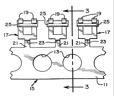
Figs. 1-6 shows one embodiment of the present invention.
As seen in Fig. 1, a long flat strip 11 of electrically conductive material
such as copper or beryllium copper is stamped into the shape of the
intermediate blank shown. This is preferably done by progressive
stamping to produce an array of a large number of repeated blanks 17
for one form of clip-holder according to the present invention.
Alternatively, the strip 11 need not be formed from electrically
conductive material, since the solder portions attached to the clips
CA 02236464 1998-05-01
WO 97/16870 PCT/US96/17704
provide the necessary conductivity to electrically connect a terminal to
a substrate or other component. The strip 11 is formed with a
longitudinally extending carrier section 15 having customary indexing or
sprocket holes 13 spaced along its length, to aid in moving the strip in
successive steps through a progressive stamping machine. The carrier
strip 15 is integral with individual clips 17 extending laterally therefrom
at regular intervals therealong, spaced correspondingly to the spacing of
terminals or pins on the electrical connectors with which the clips 17
are to be used in the manner described below. By way of example, the
clips 17 may be spaced with a pitch of 0.05 or 0.100 inch.
Integrally formed with the carrier strip 15 are a pair of
spaced fingers 19 on each clip, joined to the carrier strip 15 by a
connecting piece 21, which has a notch 23 formed therein to permit
the carrier strip 15 to be readily broken away or otherwise separated
from the sequence of clips 17. The fingers 19 are spaced apart a
distance d coordinated with the width of the pins or terminals of the
circuit element 31 (see Figs. 4 to 6) with which the clip 17 is used.
As seen in Figs. 2 and 3, a solder mass 25, preferably in
the form of a section of solder wire, is placed across the pairs of fingers
19, which are then rolled partially around the solder mass 25,
sufficiently to hold the solder in place. This is readily fabricated in the
course of the progressive stamping, by laying a solder wire 25 (which
preferably includes a solder flux) across a number of the clips 17,
curling the fingers 19 around the solder wire 25 as shown in Figs. 2
and 3, and cutting away the solder in the area between the clips 17,
leaving a solder mass 25 held by each pair of fingers 19, and of a
volume appropriate for the required soldering action.
In use, as shown in Figs. 4 and 5, a connector or other
circuit component 31 having a plurality of aligned terminals or pins 33
is passed through correspondingly spaced internally electro-plated holes
CA 02236464 1998-05-01
WO 97/16870 PCTIUS96/17704
6
35 of a substrate 37. While the substrate 37 is illustrated as oriented
vertically in Fig. 5, it will be understood that it may be horizontal or
with other orientations, as may be appropriate. A ganged strip of clips
17 of which a portion is shown in Fig. 2, with a number of clips
corresponding to the number of component terminals to be soldered to
the substrate 37, is then placed over the array of connector terminals
33 as illustrated in Fig. 4. For example, if the component 31 has 21
terminals in alignment, a section of the clip array of Fig. 4 having 21
clips will be applied over the component terminals 33 as shown, and
severed from the remainder. The separation of the fingers 19 of each
clip is selected so that there will be a frictional engagement between
each clip 17 and its corresponding connector terminal 33, so that the
strip of clips will be retained in the position shown in Figs. 4 and 5
during subsequent operations. It will be understood that where the
component 31 has two or more rows of terminals, each row of
terminals of the component 31 may be provided with a strip of the clips
of Fig. 4, although only one row is shown in Figs. 4 and B.
Then, heat is applied to the solder, as by heated air or other
conventional means, which causes the solder to reflow and to be drawn
by capillary action into the space between the terminal 33 and the sides
of the plated substrate hole 35. The hole 35 has a metallic surface, as
by being electro-plated on its interior, as indicated at 39. The plating
may extend around onto the flat surface of the substrate 37 to form
contact pads, as illustrated at 41. Normally, a slight space 43 is left
between the terminal 33 and the platinr 39 of the substrate hole 35,
into which the molten solder will be drawn. In normal practice this
space may not be deliberately provided, since the customary slight
irregularities in formation of the component terminal or the electro-
plating 39 in the hole 35 will permit the molten solder to flow
therebetween to bond the terminal 33 to the electro-plated layer 39, as
CA 02236464 1998-05-01
WO 97/16870 PCT/US96/17704
7
indicated in Fig. 6. After the soldering is completed, the carrier strip 15
is broken away from the individual clips 17 at the breakaway notches
23, leaving the clips 17 in place but soldered to the component
terminal, the plating of the hole, and to the contact pad 41. If desired,
the carrier strip may be broken away before the soldering is
accomplished, although this is not preferred.
Figure 7 shows an alternate way of using the clips of Figs.
2 and 3. In this instance, a connector or other component 31 a is
shown having two rows of terminal pins 33 instead of one row as
shown in Figure 5. In this instance the clips 17 are positioned on the
component pins 33 before the component pins 33 are inserted into the
substrate 37, and are positioned between the component 31 a and the
substrate 37. Heat is supplied as in the case of Figures 5 and 6 to join
the pins 33 to the plated hole 39 of the substrate by soldering.
Figures 8 through 12 show a modified form of the present
invention. As seen in Figure 8, the blank has a carrier strip 115 with
indexing holes 113 similar to Figure 1. Extending laterally from the
carrier strip 115 are the individual solder-holding clips 117. As seen in
Figure 8, each clip blank 117 is joined to the carrier strip 115 by a
connecting piece 121 having a breakaway notch 123. The individual
clip blank 117 includes a body portion 147 having slits 149 extending
adjacent the edges of the body portion 147 to form fingers 119 integral
at one end with the body portion 147. As indicated in Fig. 9, a solder
wire 151 (preferably including a solder flux) is laid over the successive
body portions 147 of a portion of the array of clips 117 as the array
moves along the progressive stamping apparatus. As seen in Figs. 9 to
11, the fingers 119 are then curled around the solder wire 151 to hold
it on the body portions 147. After the solder wire 151 is applied and
held by the fingers 119, holes 145 are formed as seen in Fig. 9, as by
punching through the clip bodies 147. At the same time, the solder
CA 02236464 1998-05-01
WO 97/16870 PCT/US96/17704
8
wire 151 is separated into two segments straddling each hole 145 and
a gap 153 is made in the solder wire 151 between adjoining clip bodies
147 as seen in Figs. 9 and 11. In this way, each body portion 147
carries two solder masses 125, straddling its hole 145. The holes 145
are dimensioned to engage the component terminals 133 frictionally, to
position a solder mass on either side of the respective terminal 133 as
shown in Fig. 11. In this way the array of clip bodies is retained on the
component terminals 133. The solder masses 125 remaining held by
each clip body 147 are dimensioned to provide adequate solder for
joining each clip 117 to its respective component terminal 133.
As seen in Figures 11 and 12, this form of solder-holding
clip may be used in the same manner as shown in Figures 6 or 7 or 12.
Further, the clip 117 may he used to join a component 31
or 131 with any desired further substrate or another component,
whether or not substrate 137 is present. As shown in Figures 13 and
14, the clips 117 may be formed with extensions 161 which may be
used as terminals or leads to other apparatus. For example the end of
each extension 161 may be formed into an edge clip shape 163 for a
substrate as shown in Fig. 13 and 14, to permit coupling of the
component 131 pins to a further substrate (not shown) parallel to the
component 131 or in alignment thereto. By bending extension 161 at
right angles, the further substrate may be perpendicular to substrate
137. In place of edge clip 163, the end of each extension 161 may be
formed for surface mounting to a substrate contact pad, or may have
any other desired configuration. -
Figures 15-18 show a further modification of the present
invention. In this instance, each solder-holding clip 219 is formed with
a pair of sides 201 joined by a back 203. Each side 201 has a pair of
fingers or tabs 205 extending partially around a solder mass 225,
leaving a space 207 between the solder mass 225 and the back 203,
CA 02236464 1998-05-01
WO 97/16870 PCT/US96/17704
9
for receiving a terminal pin 209 of a connector 211. Alternatively,
preferably the spacing between the arms 201 is dimensioned to
frictionally engage the pins 209. As shown in Figure 18, the pin 209
passes through a substrate 213, having an internally plated hole and/or
a conductive pad to which the pin 209 is to be soldered.
This form of invention also-is adapted for multi-stage
progressive stamping. In fabrication, an elongated strip of conductive
material is stamped as shown in Figure 15 to have a carrier strip 215
with a series of the clips 219 extending laterally therefrom. The body
is bent into the U-shape shown in Figure 17 to form clip sides 201 each
with a pair of tabs or fingers 205. A solder wire 225 of a diameter
conforming to the separation between the pairs of fingers 205 is laid
between the pairs of fingers 205, and the fingers are then bent partially
around and staked into the solder wire 225. The solder wire 225 is then
cut between the clips 219, leaving an aE-nount of solder appropriate for
the specific use for the clips. A connecting portion 221 serves to join
the clip 219 to the carrier strip 215, and- is bent with an offset as
shown in Figures 17 and 18, so that when assembled to a row of
terminals 209, interference is svoided between the terminal pins 209a
and 209b and the carrier strip 215.
The spacing between the clips 209 is correlated to the
spacing between the pins 209a or 209b of the connector 211, so that
in use a section of the strip of Figure 15 having a number of clips 219
equal to the number of pins 209 in a row of the connector 211, may be
inserted over the pins 209 as shown iri dashed lines 209 in Figure 15
and also in Figure 18. Figure 18 shows connectors 211 illustratively of
the dual row type, having terminal pins '209a and 209b equally spaced
in the direction perpendicular to the plane of the paper. It will be
understood that the present invention may be used with any number of
rows of terminal pins, from one row up. By way of illustration, the
CA 02236464 1998-05-01
WO 97/16870 PCTIUS96/17704
.
connectors 211 may be of the J 1 or J2 type, and the substrate 213
may be a PC104 board. Illustratively the terminals 209 may be spaced
at 0.100 inch intervals, and the pins may be 0.480 inches long with a
0.025 inch square cross section.
5 Upon reflowing, the solder will flow around the pins 209
and by capillary action into the internally plated holes of the substrate
213. After the soldering is completed, each clip has its joining section
221 broken or cut off, as by a notch 223 formed therein.
The solder-holding clips of the present invention are usable
10 not only to solder a connector or other component having non-solder-
bearing terminals to through-plated holes of a substrate, but may also
be used to solder a lead having any desired terminal configuration to a
pin or other terminal of an electrical component. Fig. 19 shows the
lead clip 219 with its lead 221 bent out at a right angle to terminal pin
209, and terminated in a solder-holding arrangement 250 to permit
surface mounting of connector 211 on a substrate (not shown). The
solder-holding arrangement may have any appropriate construction,
such as shown in U.S. Patent No. 4,679,889.
Referring now to Fig. 20, therein is shown an alternative
embodiment of the present invention, which is similar to that shown in
Figs. 1-6. However, as seen in Fig. 20, clip 317 is provided with two
pairs of fingers 319, with one pair of fingers being located on the side
of clip 317 adjacent carrier strip 15, and the other pair of fingers being
located on the opposite side of clip 317. Clip 317 has a generall double
l-shape, which may be formed by a progressive stamping operation.
Two solder portions 321 are positioned laterally across the two pairs of
fingers 319. The solder portions 321 may be formed in much the same
manner as solder wire 25 (Fig. 2).
Each pair of fingers 319 is then curled around the
corresponding solder portion 321 to thereby securely retain the solder
CA 02236464 1998-05-01
WO 97/16870 PCTIUS96/17704
11
portion 321 (Fig. 21). As shown in Fig. 20, the solder sections 321
extend partially into the central aperture in clip 317. Referring now to
Fig. 22, therein is shown a connector or other circuit component 31
having a plurality of pins 33, with each of the pins 33 passing through
the central aperture of a corresponding clip 317. Because the solder
portions 321 extend partially into the central aperture, they act to
frictionally engage the inserted pin 33. After the clips 317 are
positioned on the connector 31, the pins 33 are subsequently inserted
into corresponding holes 35 of a substrate 37. Heat is then applied,
which causes the solder sections 321 to reflow and be drawn into the
space between the terminals 33 and the sides of the holes 35 (Fig. 23).
Although the clip 317 shown in Figs. 20-23, is shown as being
positioned between the connector 31 and substrate 37, the clip 317
may also be iased where it is positioned after the substrate 37 is mated
with the clip 317, similar to Fig. 5. -
Referring now to Fig. 24, therein is shown the use of a pair
of clips 219 (after the removal of connecting portion 221) for soldering
a pair of pins 33 on a connector 31 to a pair of contact pads 350
positioned on opposite sides of a substrate 37. Effectively, the pair of
clips 219 provide a "straddle mount" between the connector pins 33
and the substate 37. As shown in Fig. 24, the clips 219 are positioned
with their solder portions 225 facing each other. The connector pins
33 are then inserted into the opposed clips 219, and the substrate is
positioned in between clips 219 so as to be frictionally engaged by the
opposed solder portions 225. Heat is applied, as described above, to
cause the solder to reflow. The clips 219 may be provided as a pair of
arrays to thereby solder an edge connector to two rows of contact
pads, wherein each row is positioned on opposite sides of the substrate
37.
It will be understood that the solder elements 25, 125, 151
CA 02236464 1998-05-01
WO 97/16870 PCT/US96/17704
,12 .
and 321 may incorporate customary solder flux to facilitate the proper
soldering operation.
While the solder-holding clips of the present invention are
illustratively described as used with the terminals of a connector, it will
be understood that these clips may be used in joining terminals of
integrated circuit chips, chip holders, resistors, capacitors and other
non-solder bearing electrical components"to contact pads or plated
holes of printed circuit boards or other substrates.
The foregoing embodiments should be understood as
exemplary only, the present invention being defined by the following
claims.