Note: Descriptions are shown in the official language in which they were submitted.
CA 02236788 1998-0~-0~
WO 97/17302 PCT/US9S/14654
FIELD-ASSISTED SEALING
This application relates to a method of bonding glass
.
substrates to other nonconductive substrates and to the bonded products.
The invention has its genesis in attempts to solve the
5 problem of bonding glass plates on which microstructures, such as channels
for conveying fluids, which channels have widths, for instance, between
about 50 and about 150 microns, and similarly scaled depths, have been
fabricated. A method that well preserved such structures was sought.
Field-assisted thermal bonding was initially rejected as an option because this
method has never been satisfactorily applied to a nonconductive material such
as glass. However, the present inventors have discovered parameters that
allow hermetic sealing between glass plates using this methodology.
It will, of course, be recognized that the invention has broad
applicability and is not limited to the particular problem that gave rise to theinvention. For instance, it can be used in the manufacture of (i) sensors
(including both physical and chemical sensors), (ii) micropumps and
microvalves, (3) microelectric mechanical systems, and (iv) miniaturized
diagnostic or other analytic devices.
SUMMARY OF THE INVENTION
The invention provides method of bonding a glass substrate
and a nonconductive substrate comprising the steps of: (a) contacting a
surface of the nonconductive substrate which is coated with a field-assist
bonding material with a conforming surface of the glass substrate; and (b)
applying sufficient heat to the two substrates and sufficient voltage across
25 the two substrates to bond the two substrates together.
BRIEF DESCRIPTION OF THE DRAWINGS
Figure 1 shows a device for conducting field-assisted
bonding of glass substrates.
Figure 2 displays a cut-away view of a liquid distribution
- 30 system that can be used with the invention.
Figure 3 displays a distribution plate of the liquid distribution
system of Figure 2.
CA 02236788 1998-0~-0~
WO 97/1730;! PCT/US95/14654
Figure 4 displays an expanded view of a portion of the
distribution plate of Figure 3.
DEFINITIONS
The following terms shall have the meaning set forth below:
~ annealing the temperature at which the internal stress in a
temperature glass begins to be substantially reduced.
~ capillary dimensions dimensions that favor capillary flow of a liquid.
Typicaily, channels of capillary dimensions are
no wider than about 1.5 mm. Preferab!y
channels are no wider than about 500 ,um, yet
more preferably no wider than about 250 ,um,
still more preferably no wider than about
1 50,~m.
~ glass any of a number of materials commonly referred
to as "glass" that contain a silicon oxide
structure .
~ hole diameter because techniques for fabricating small holes
often create holes that are wider at one end
than the other (for instance, about 50 microns
wider), the hole diameter values recited to herein
refer to the narrowest diameter.
~ horizontal, vertical, indications of the orientation of a part of the
EW, NS distribution system refer to the orientation when
the device is in use. The notations "EW axis"
and "NS axis" are in reference to Figures 3 and
4, where an EW axis goes from right to left and
- is perpendicular to the long axis of the page anda NS axis is from top to bottom parallel to the
long axis of the page.
CA 02236788 1998-0~-0~
WO 97/17302 PCT/~JS95/14654
~ nonconductive made of a material having an electrical
substrate resistance that is at least about as high as such
traditional insulators as one of glass or ceramics.
~ perpendicular channels in the distribution plate are
perpendicular even if primarily located on
separate horizontal planes if their vertical
projections onto the same horizontal plane are
perpendicular.
~ reservoir unless a different meaning is apparent from the
context, the terms "reservoir" and "fluid
reservoir" include the horizontal extension
channels (sometimes simply termed
"extensions") directly connected to the reservoir
or fluid reservoir~
DETAILED DESCRIPTION
A. Bonding Substrates
The method of the invention of permanently joining glass
substrates uses a field-assisted thermal bonding process. It has now been
discovered that glass-glass sealing using field-assisted thermal bonding is
10 possible despite the low conductivity of glass if a field-assist bonding material
is interposed between the substrates to be bonded.
To the top or bottom surface of one glass substrate, a layer
of a field-assist bonding material is applied. Preferably, the field-assist
bonding material layer has a thickness from about 50 nm to about 1,000 nm,
15 more preferably from about 150 nm to about 500 nm. The field-assist
bonding material can be a material capable of bonding a glass substrate to
another substrate using the method of the invention. Preferably, the
~, field-assist bonding material is capable of forming covalent bonds with silicon
- oxide. Preferably, the field-assist bonding material is nonconductive.
20 Preferably, the field-assist bonding material is non-doped silicon or silica.More preferably, the field-assist bonding material is non-doped silicon.
CA 02236788 1998-0~-0~
WO 97/17302 PCT/US95/14654
The field-assist bonding material can be app~ied to a
nonconductive substrate, for instance, by electron beam evaporation (where
electrons bombard a source materlal to vaporize atoms that are then
condensed on a substrate), chemical vapor deposition or by a sputtering
5 process (where surface molecules are emitted from a cathode when the
cathode is bombarded with positive ions from a rare gas discharge and the
emitted surface molecules collide with and bond to a nearby substrate).
Pursuant to the present invention, silicon layers of from about 150 nm to
about 500 nm thickness have been deposited on glass substrates under
10 atmospheric conditions that can be expected to generate an outer surface
layer of silicon dioxide, such as an about 20A layer. In one embodiment, the
outer silicon dioxide layer is from about 15 A to about 30 A in thickness. The
coated nonconductive substrate is treated, as needed, to create channels,
reservoirs, or reaction cells using etching or laser ablation techniques.
15 Alternatively, such microstructures can be formed in the nonconductive
substrate prior to coating with the field-assist bonding material. The coated
substrate is then positioned against a glass substrate with a shape that
conforms to the shape of the coated, nonconductive substrate. The glass
substrate preferably is not coated with the field-assist bonding material on the20 surface that will be bonded. The two substrates are placed in a field-assisted
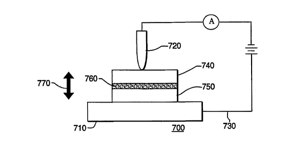
bonding device 700 such as that illustrated in Figure 1. The field-assisted
bonding device 700 has a heating device 710, such as a heating plate or
furnace. The field-assisted bonding device 700 further has an electrode 720
and a ground 730 that allows a voltage to be applied across the glass
25 substrate 740 and the nonconductive substrate 750, to which has been
applied a layer of silicon 760. Arrows 770 indicate the electric field
orientation. Generally, the field-assisted bonding is conducted under a normal
atmosphere.
The two substrates are brought to a temperature effective to
30 bond the two substrates together when an appropriate electric field is applied
across the plates effective to accelerate the bonding process. While not
wishing to be bound by theory, it is believed that the combination of ~1) an
CA 02236788 1sss-o~-o~
wo 97/17302 PCT/US95/14654
electrode 720 applied to the glass substrate 740 and (2) the~greater
exchange-site mobility of ions (such as sodium ions) caused by the eievated
temperature causes an ion depletion (such as a sodium ion depletion) on the
face of the glass substrate 740 opposite that to which the cathode is applied.
5 The ion depletion, it is believed, causes a surface charge at the bottom
surface of glass substrate 740, which correlates with the creation of a strong
localized electrostatic attraction for the nonconductive substrate 750. It is
clear that this process creates strong bonding between the substrates and, it
is believed that this is due to the formation of chemical bonds between the
10 silica of the glass substrate 740 and the silicon coated onto the
nonconductive substrate 750. Preferably, the electrode 720 is a cathode.
Preferably, the temperature is brought to from about 200~C to about 600~C,
more preferably from about 300~C to about 450~C. Alternatively, the
temperature is brought to from about 200~C to about 50~C less than the
15 annealing temperature of the glass being handled, preferably from about
200~C to 150~C less than the annealing temperature. During the process an
voltage typically from about 200 V to about 2,500 V, preferably from about
500 V to about 1,500 V, is applied across the first glass substrate 740 and
second glass substrate 750. The voltage most suitably applied varies with
20 the thickness of the substrates. The voltage pulls the glass substrate 740
and nonconductive substrate 750, including the silicon layer 760 applied to
one of the substrates, into intimate contact. Typically, hermetic sealing is
achieved within minutes to about one hour, depending on the planar
dimensions of the glass substrates. The time required to achieve adequate
25 sealing varies with, among other things, the smoothness of the substrates,
the conformity of the surfaces of the glass substrates to be bonded, the
electrical field strength, the temperature, and the dimensions of the
substrates. Bonding between the substrates is typically apparent visually,
since it is accompanied by the disappearance of the optical interface pattern
~ 30 (e.g. rainbow pattern) created at the junction between the substrates and the
formation of gray color at the bonded regions that can be seen when an
observer looks through the two substrates.
CA 02236788 1998-0~-0~
WO 97/17302 PCT/US95/14654
Corning 1735 boroaluminosiiicate glass, and Corning 7740
borosilicate glass (PyrexTM, annealing temperature = 560~C), available from
Corning Glass Co., Corning, NY, are among the preferred glasses for use in
this invention. Other glasses, including soda lime glass, are suitable.
5 Substrates, preferably plates, having a thickness of from about 0.2 mm to
about 5 mm, preferably from about 0.5 mm to about 2 mm are particularly
suitable. Preferred silicon materials for use as the field-assist bonding material
are pure, non-doped, densely packed and have amorphous structure. The
nonconductive substrate is preferably glass or aluminum oxide. Most
10 preferably, the nonconductive substrate is glass.
The method of the invention can be used to bond a glass
substrate to another glass substrate and to a nonconductive substrate
simultaneously. In a preferred embodiment, the invention is used to
simultaneously bond three glass substrates.
Those of ordinary skill will recognize that while a hot plate is
illustrated as providing the heating for the thermal assisted bonding, other
heating devices, including ovens, may be used. It will also be realized that it is
desirable to match, when possible, the coefficients of thermal expansion of
the substrates to be bonded.
B. Liquid Distribution Svstem
One version of the liquid distribution system 100 that gave
rise to the invention is illustrated in Figures 2-4. The distribution system is
formed of at least three plates, a feedthrough plate 300, a distribution plate
310 and a reaction cell plate 320 (Figure 2). The feedthrough plate 300 is
bonded to the distribution plate 310 using the method of the invention. The
feedthrough plate 300 has multiple first electrodes 360 and second electrodes
361. The reaction cell plate 320 is typically removably fitted to the underside
of the distribution plate 310, or the underside of intermediate plate 330
interposed between the distribution plate 310 and the reaction cell plate 320. ~-
Figure 3 shows the layout of a distribution plate 310
according to the invention. Figure 4 shows an expanded view of a portion of
a distribution plate 310 that better illustrates some of the features obscured
CA 02236788 1998-0~-0~
WO 97/17302 PCT/US95/14654
by the scale of Figure 4. Typically, the structures indicated 1~ solid lines will
be formed in the top layer of the distribution plate 310, while the structures
indicated with dotted lines will be formed in the bottom layer of the
distribution plate 310, except that in Figure 2 the reaction cells 350 are
5 indicated by boxes in solid lines even though these structures are located in a
lower plane . Where appropriate, vertical channels connect the structures in
the top of the distribution plate 310 with those in the bottom.
At the top of Figure 3 are four first fluid reservoirs 200A,
200B, 200C and 200D, each having a defined fill level. Each of these first
10 fluid reservoirs 200A, 200B, 200C and 200D has two first reservoir
extensions 212 extending along substantially all of an EW axis ~see
definitions) of the distribution plate 310. The ceilings of the first reservoir
extensions 212 preferably are at substantially the same elevation as the first
fill level. At five staggered locations, A1, B1, C1, D1 and E1, along the EW
15 axis of the first reservoir extensions 212 there are four first vertical channels
214 (not shown) that connect the first reservoir extensions 212 with four
first horizontal feeder channel segments 216 that are formed in the bottom
layer of the distribution plate 310. At each staggered location A1, B1, C1,
D1 or E1, four adjacent first horizontal feeder channel segments 216, which
20 are connected to separate first reservoir extensions 212, extend along an NS
axis to ten positions, A2, B2, C2, D2, E2, F2, G2, H2, 12 and J2. Each
position A2, B2, C2, D2, E2, F2, G2, 12 or J2 along the course of each such
set of four adjacent horizontal feeder channel segments 216 is adjacent to a
pair of reaction cells 350 (not shown). At these positions A2, B2, C2, D2,
25 E2, F2, G2, H2, 12, or J2, the four adjacent first horizontal feeder channel
segments 216 are separately connected, via separate second vertical
channels 225 (not shown), to each of four perpendicular first distribution
channels 222 formed in the top layer of the distribution plate 310. The
ceilings of the first distribution channels 222 define a second fill level that is
- 30 typically substantially the elevation of the first fill level. The fill level of a
distribution channel (e.g., the second fill level) is "substantially" the fill level
of the connected reservoir (e.g., the first fill level) if they are offset vertically
CA 02236788 1998-0~-0~
WO 97/17302 PCT/US95/14654
by no more than about 10% of the depth of the channel; even if the fill levels
are further offset vertically they are still substantially the same if filling the
reservoir to its fill level results in filling the connected distribution channel and
the retention of fluid in the connected distribution channel. The combination
5 of a first vertical channel 214, connected to a horizontal feeder channel
segment 216, in turn connected to a second vertical channel 225 makes up a
first feeder channel 217 (not identified in the Figures).
If liquids are maintained at a defined first level in a first fluid
reservoir 200, then substantially the same level will be maintained in the first10 distribution channels 222 connected to that first fluid reservoir 200 via first
feeder channels 217. This equalization occurs due to the principle that two
connected bodies of liquid will tend to seek the same level and, where the
size of the channels allows, due to capillary flow. Liquids are maintained at a
defined level in the first fluid reservoirs. In the illustrated embodiment, liquid
15 is fed into the fluid reservoir 200 through channels in the feedthrough plate300 and such liquid that is not needed to fill the fluid reservoirs to the defined
level is drained through drains 380. First openings 381 (not shown) are
formed in the bottom layer of the feedthrough plate 300 to create a liquid
connection or sluice between the first fluid reservoirs 200 and the drains 380.
20 Liquids are constantly feed into the first fluid reservoirs 200 ~as well as the
second fluid reservoirs 210 and third fluid reservoirs 220) typically by the useof an external pump 15 (not shown), such as the model number 205U
multichannel cassette pump available from Watson-Marlow, Inc.
~Iternatively, a defined level can be maintained by monitoring the level of
25 liquid in the first fluid reservoirs 200 (or second fluid reservoirs 210 or third
fluid reservoirs 220) and only activating the pumps feeding liquid to a given
fluid reservoir when needed to maintain the defined level.
Each set of four adjacent first distribution channels 222 are
adjacent to two buffer channels 218, located to each side of the first
-30 distribution channels 222 along the EW axis. Liquid can be pumped from any
first distribution channel 222 into the adjacent buffer channel 218 by
activating the first pump 360 (indicated in Figure 4 by two filled dots
~ , _ . ,
CA 02236788 1998-0~-0~
WO 97/17302 PCT/US95/14654
representing the electrodes of one type of pump) of the first distribution
channel 222. This pumping creates additional pressure that moves the liquid
over capillary barrier 370 (not shown) separating the first distribution channel222 and the buffer channel 218. Between each first distribution channel
5 222, second distribution channel 224 or third distribution channel 226 and
the adjacent buffer channel 218 and between each buffer channel 218 and its
adjacent third vertical channel 390 (described below) there is such a capillary
barrier 370 that inhibits liquid flow when the pumps are not activated.
Second openings 362 (not shown) are formed in the bottom layer of the
10 feedthrough plate 300 to create a liquid connection or sluice between the first
distribution channels 222 and the buffer channels 218. From a buffer
channel 218, liquid can be pumped using a second pump 361 (indicated in
Figure 4 by two filled dots representing the electrodes of one type of pump)
to a third vertical channel 390 that connects with a reaction cell in the
15 reaction cell plate 320. Third openings 363 Inot shown) in the bottom layer
of the feedthrough plate 300 or the distribution plate 310 serve to create a
liquid connection or sluice between the buffer channels 218 and third vertical
channels 390.