Note: Descriptions are shown in the official language in which they were submitted.
CA 022369~ 1998-0~-06
WO 97/17706 PCT/US96/17732
-~n CONDUCTOR8 coN~r~TNTNG ANI80T~OPIC 8UP~rQNT~UCTING
COMPOUND8 AND N~ ~ Ol~ FOR M~RTr'-- THEM
Field of the Invention
This invention relates to superconducting cabled
conductors and to a method for manufacturing them.
Background of the Invention
The possibility of using superconductors to obtain
greater efficiency in electrical and magnetic
10 applications has attracted considerable interest,
particularly since the discovery of superconducting
materials, such as the oxide superconductors, whose
structures allow them to carry significant currents at
relatively high temperatures, above about 20 Kelvin.
15 However, to be practical outside the laboratory, most
electrical and magnetic applications require flexible
cabled lengths of conductor manufacturable with high
packing factors at reasonable cost, in addition to high
engineering current-carrying capacity.
High packing factor forms ~;~;ze performance per
unit volume. Space constraints and the need to handle
higher overall current densities are among the major
design issues considered in most electrical applications.
Conductors which are flexibly cabled, that is,
25 composed of twisted, helically wound, braided or
otherwise transposed bundles of mechanically and
electrically isolated conductor strands, are desired in
many applications, including coils, rotating machinery
and long length cables. In comparison to monolithic
30 conductors of comparable composition and cross-section,
cabled forms which are made from a number of conductor
~ strands which are substantially mechanically isolated
will have much higher flexibility. By substantially
CA 022369~ 1998-0~-06
WO97/17706 PCT~S96/17732
mechanically isolated is meant that the cable strands
have some ability to move independently within the cable,
although a degree of mechanical locking of the strands is
usually desired for stability and robustness.
5 Flexibility increases in proportion to the ratio between
the cable cross-section and the strand cross-section.
In low temperature metallic superconducting
conductors, cables which are made from a number of
substantially electrically isolated and transposed
lO conductor strands have been shown to have greatly reduced
AC losses in comparison to monolithic conductors cf
"Superconducting Magnets" by Martin Wilson (1983,1990),
pp 197, 307-309, and it has been proposed that the same
relation will hold for high temperature superconductors
15 with more complex structures. AC losses are believed to
decrease in relation to strand cross-section, cable
cross-section and twist pitch. Litz cable, a cable with
multiple electrically insulated strands assembled in a
fully transposed configuration, is required for nearly
20 all AC applications. For DC applications, multiple
uninsulated strands may be cabled to obtain flexibility
or m~ch~n;cal robustness. The greater the number of
strands in the cable, the more pronounced these
advantages will be. Cabling is also desirable for ease
25 in manufacturing, since cabling processes scale more
easily than monolithic manufacturing processes.
However, most of the superconductors, such as
superconducting ceramics of the oxide, sulfide, selenide,
telluride, nitride, boron carbide or oxycarbonate types,
30 which have shown promise for electrical and magnetic
applications at relatively high temperatures are
anisotropic superconducting compounds which re~uire
texturing in order to optimize their current-carrying
capacity. It has not been considered feasible to form
35 these into high packing factor, tightly transposed cable
CA 022369~ 1998-0~-06
WO97/17706 PCT~S96/17732
configurations because of the physical limitations of
these materials. They typically have complex, brittle,
granular structures which cannot by themselves be drawn
into wires or similar forms using conventional metal-
5 processing methods and do not possess the necessarym~Gh~n; cal properties to withstand cabling in continuous
long lengths. Consequently, the more useful forms of
high temperature superconducting conductors usually are
composite structures in which the anisotropic
lO superconducting compound is supported by a matrix
material which adds mechanical robustness to the
composite. For example, in preferred manufacturing
processes for superconducting oxide composites, such as
the well-known powder-in-tube (PIT) process or various
15 coated conductor processes, the desired superconducting
oxide is formed within or on a supporting matrix,
typically a noble metal, by a combination of phase
transformation and oxidation reactions which occur during
the manufacturing process.
Even in composite forms, the geometries in which
high-performance superconducting articles may be
successfully fabricated from these materials are
constrained by the necessity of "texturing" the
superconducting ceramic to achieve adequate critical
25 current density and by the electrical anisotropy
characteristic of the superconductor. The current-
carrying capacity of any composite containing one of
these materials depends significantly on the degree of
crystallographic alignment, known as "texturing", and
30 intergrain bonding of the superconductor grains , induced
during the composite manufacturing operation. For
example, the rare earth family of oxide superconductors,
among the most promising and widely studied of the
ceramic superconductors, require biaxial texture, a
35 specific crystallographic alignment along two axes of
CA 022369~ l998-0~-06
WO97/17706 PCT~S96/17732
each grain, to provide adequate current carrying
performance Certain ceramic superconductors with
micaceous crystal structures, such as the two-layer and
three-layer phases of the bismuth-strontium-calcium-
5 copper-oxide family of superconductors (Bi2Sr2CalCu2Ox, t
also known as BSCCO 2212, and Bi2Sr2Ca2CU3Ox, also known
as BSCCO 2223), demonstrate high current-carrying
capacity when uniaxially textured in the plane
perpendicular to the current carrying direction.
lO (Micaceous structures are characterized by highly
anisotropic, plate-like grains with well-defined slip
planes and cleavage systems.) In addition, many
superconducting compounds may be partially textured by
uniaxial texturing tech~;ques. Those anisotropic
15 superconducting compounds which are suitable for uniaxial
texturing techniques have been considered especially
promising for electrical applications because they can be
textured by methods which are readily scalable to long
length manufacturing.
In contrast to other known conductors, such as the
normal and superconducting metals, the current carrying
capacity of well-textured anisotropic superconducting
composite articles will depend in large part on the
relative orientations of their preferred direction, which
25 is determined by the crystallographic alignment of their
superconducting grains, and any current flow or external
magnetic field. Because of their crystal structure,
supercurrent flows preferentially in at least one of the
directions lying within the plane normal to the c axis of
30 each grain. Their critical current may be as much as an
order of magnitude lower in their "bad" direction than in
their "good" direction. Thus, an important consideration
in fabricating high performance cables from these
materials, which is not an issue in conventional cable
35 fabrication, is finding a way to ~;~;ze the portions of
CA 022369~ l998-0~-06
WO97/17706 PCT~S96/17732
-
the cable which do have the desired orientations. For
optimum current-carrying capacity, it would be desirable
to align all of the grains in the cable in parallel to
one another along their relevant axes, e.g., at least the
5 c axis for the uniaxial texturing typical of BSCCO 2212
or 2223, or at least the c axis and either the a axis or
the b axis for the biaxial texture typical of the rare
earth superconducting oxides, with each c-axis preferably
perpendicular to the longitudinal axis of the cable
lO regardless of the relative rotational orientations of the
cable strands and filaments which contain them, but the
twisting and bending characteristic required for
conventional cabling are not readily adaptable to such
uniform grain alignment.
Thus, an object of this invention is to provide a
textured cabled conductor containing a textured
anisotropic superconducting compound having substantial
crystallographic grain alignment which is directionally
independent of the rotational orientations of the strands
20 and filaments in the cabled conductor, and a process for
manufacturing such a cabled conductor.
Another object of the invention is to provide a
novel cabled conductor manufacturing process that will
allow strands of superconducting compounds which require
25 texturing to be used with conventional high-speed cabling
equipment.
Another object is to provide a mechanically
stable, fully transposed high packing factor cabled
conductor containing anisotropic superconducting
30 compounds in a plurality of strands which may be highly
aspected, and a method for manufacturing such a cabled
conductor.
Another object of the invention is to provide a
high packing factor, well-textured cabled conductor
35 comprising a plurality of strands each comprising a
CA 022369~ 1998-0~-06
WO97/17706 PCT~S96/17732
micaceous or semi-micaceous superconducting oxide, most
preferably BSCCO 2223 and a method for manufacturing such
a cabled conductor.
SUMMARY OF THE INVENTION
In one aspect, the invention provides a cabled
conductor comprising a plurality of transposed strands
each comprising one or more preferably twisted filaments
preferably surrounded or supported by a matrix material
and comprising textured anisotropic superconducting
lO compounds which have substantial crystallographic grain
alignment that is substantially unidirectional and
directionally independent of the rotational orientation
of the strands and filaments in the cabled conductor. In
another aspect, the invention provides a transposed
15 cabled conductor comprising grains of anisotropic
superconducting compounds textured such that the
crystallographic c axis alignment of each grain of the
superconducting compound is substantially perpendicular
to the longitll~; n~ l axis of the cabled conductor
20 independent o~ the rotational orientation o~ the strands
and filaments in the cabled conductor. The filaments are
preferably surrounded or supported by a matrix material.
The invention may be practiced with any
anisotropic superconducting compound which re~uires
25 texturing of its grains. The compounds are preferably
superconducting ceramics of the oxide, sulfide, selenide,
telluride, nitride, boron carbide or oxycarbonate types,
and most preferably superconducting oxides. By "grains"
are meant polycrystalline colonies in which the c axes
30 are substantially coincident and the a and b axes have a
multiplicity of orientations for colony-forming
superconducting compounds, such as the micaceous
superconducting oxides, and single or polycrystalline
regions in which the a, b, and c axes are substantially
CA 022369~ 1998-0~-06
WO97/17706 PCT~S96/17732
coincident for those compounds which do not form
colonies.
In another aspect, the invention provides method
for manufacturing a superconducting cabled conductor
~ 5 comprising the steps of, first, forming a plurality of
composite strands, each strand comprising at least one,
preferably twisted, filament having a preselected
filament cross-section and twist pitch, preferably
surrounded or supported by a matrix material, and
lO containing grains of a desired anisotropic
superconducting compound or its precursors; second,
forming a cabled intermediate from the strands by
transposing them about the longitudinal axis of the
conductor at a preselected strand lay pitch, and,
15 texturing the strands in one or more steps including at
least one step involving application of a texturing
process with a primary component directed orthogonal to
the widest longitudinal cross-section of the cabled
intermediate, and if a precursor to the desired
20 superconducting compound remains, at least one
thermom~h~n;cal processing step at conditions sufficient
to produce phase transformation in the filament material,
at least one such orthogonal texturing step occurring
subsequent to said strand transposition step; thereby
25 forming a superconducting cabled conductor having a
crystallographic grain alignment substantially
independent of the rotational orientation of the strands
and filaments in the cabled conductor. In a preferred
embodiment, the filament cross-section, filament twist
30 pitch, and strand lay pitch are cooperatively selected to
provide a filament transposition area which is always at
least ten times the preferred direction area of a typical
grain of the desired anisotropic superconducting
compound. For materials requiring biaxial texture, the
35 texturing step preferably includes application of a
CA 022369~ l998-0~-06
WO97/17706 PCT~S96/17732
texturing process with a primary component in a
predetermined direction in the plane of the widest
longitudinal cross-section of the conductor.
In a preferred embodiment of the invention, the
5 invention is practiced with superconducting ceramics
which are themselves micaceous or semi-micaceous, or
which have micaceous or semi-micaceous precursors, and
the texturing step preferably includes non-axisymmetric
deformation texturing with a primary component of the
lO force tensor directed orthogonal to the widest
longitudinal cross-section of the cabled intermediate.
By "micaceous" is meant characterized by highly
anisotropic preferred cleavage planes and slip systems,
and therefore highly anisotropic current-carrying
15 capacity. By "semi-micaceous" is meant characterized by
a highly anisotropic grain structure but poorly defined
cleavage planes and slip systems. By "precursor" is
meant any material that can be converted to a desired
anisotropic superconductor upon application of a suitable
20 heat treatment. If the desired anisotropic
superconductor is an oxide superconductor, for example,
precursors may include any combination of elements, metal
salts, oxides, suboxides, oxide superconductors which are
intermediate to the desired oxide superconductor, or
25 other compounds which, when reacted in the presence of
oxygen in the stability field of a desired oxide
superconductor, produces that superconductor.
In a preferred embodiment, the desired
superconducting compound is surrounded or supported by a
30 matrix, preferably a metal. By "matrix" as that term is
used herein, is meant a material or homogeneous mixture
of materials which supports or binds a substance,
specifically including the superconducting compounds or
their precursors, disposed within or around the matrix.
35 Silver and other noble metals are the preferred matrix
CA 022369~ 1998-0~-06
WO97/17706 PCT~S96/17732
materials, but alloys substantially comprising noble
metals, including ODS silver, may be used.
In a preferred embodiment, each strand may be
coated with a layer of an insulating material prior to
5 cabling so that the strands in the finished cable will be
electrically discrete. By "insulating material", as that
term is used herein, is meant a material with an
electrical resistivity high in comparison to that of the
matrix material used in the composite under the intended
lO conditions of use.
In the most preferred embodiment of the invention,
the desired anisotropic superconducting compounds are
members of the bismuth family of superconducting oxides,
and the orthogonal texturing step preferably includes
15 non-axisymmetric deformation texturing with a primary
component of the force tensor directed orthogonal to the
widest longitn~;n~l cross-section of the cabled
intermediate. In addition, because members of the
bismuth family tend to selectively form grains aligned
20 with the filament walls, at least one additional
requirement is included in the process to overcome this
tendency. In one embodiment of the invention, this
requirement is that the filament cross-section, filament
twist pitch, and strand lay pitch be cooperatively
25 selected so that at each point on the filament,
regardless of how it is twisted, the filament width in
the plane of the widest longitudinal cross-section of the
conductor which is always greater than, and preferably
twice as large as the filament height orthogonal to the
30 widest longitudinal cross-section of the conductor. In
another embodiment of the invention, this additional
requirement is a magnetic alignment step with a primary
component of the field directed orthogonal to the widest
- longit-l~; n~ 1 cross-section of the cabled intermediate.
35 The magnetic alignment step may be done anytime after
CA 022369~ l998-0~-06
WO97/17706 PCT~S96/17732
-- 10 --
cabling. In a preferred embodiment, one or more heat
treatment steps at conditions chosen to provide crack
healing in the filaments but not to melt the matrix
material may be incorporated into the process to increase
5 the overall strain tolerance and performance of the
cabled conductor.
By "low aspect ratio" is meant an aspect ratio
less than about 2:1, and by "high aspect ratio" is meant
an aspect ratio greater than or equal to about 3:1 and
lO preferably about 5:1.
BRIEF DESCRIPTION OF THE DRAWINGS
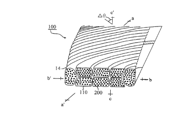
FIG 1 is a perspective view showing a
superconducting cabled conductor, lOO in accordance with
one aspect of the invention.
FIG 2 is an expanded cross-section of the
composite strand 120 shown in FIG 1.
FIG 3 is an expanded cross-section of the filament
200 shown in FIGS 1 and 2.
Fig 4 is a chart of a mosaic spread typical of a
20 well-textured anisotropic superconducting compound.
Fig 5 is a schematic representation of a cabling
machine.
DET~Tr~r~n DESCRIPTION OF THE PREFERRED EMBODIMENTS
Referring now to Fig 1 of the drawings, a
25 superconducting cabled conductor lOO manufactured in
accordance with one embodiment of the invention, is shown
in cutaway perspective view. In Fig 1, line a-a' defines
the longitudinal axis of the conductor, line b-b' defines
the major axis of its vertical cross-section, and line c-
30 c' defines the minor axis of its vertical cross-section.
Line c-c' is orthogonal to the preferred current
direction for the conductor, which flows in the a-b
plane. Lines a-a' and b-b' together define the widest
CA 022369~ l998-0~-06
WO97/17706 PCT~S96/17732
longitudinal cross-section 14 of the conductor. The
cabled conductor 100 comprises a plurality of strands 110
transposed about the longitudinal axis of the conductor.
In Fig 2, a strand 110 is shown in expanded
5 cross-section. Each strand comprises one or more
substantially continuous filaments 200 comprising grains
of a desired anisotropic superconducting compound. For
AC applications, it is preferred that the filaments be
twisted. In the preferred embodiment shown, each
10 filament 200 is supported or surrounded in a matrix
material 220. Referring now to Fig 3, each grain 210 of
the desired anisotropic superconducting compound has a
length 10, a width 11 and a thickness 12, with the length
and width being roughly the same order of magnitude.
15 Typically, the preferred direction of superconducting
current flow is perpendicular to the thickness of the
grain. Thus, the preferred direction area 13 of the
grain 210 is the product of its length 10 and its width
11. For the micaceous and semi-micaceous compounds which
20 are preferred for the operation of this invention, the
grain thickness 12 will typically be substantially less
than either the length 10 or width 11. For optimal
current flow, it is desirable that the grains 210 have
substantially unidirectional crystallographic alignment
25 with their thicknesses 12 substantially uniformly
oriented in a single direction orthogonal to the widest
longitudinal cross-section of the cable. This direction,
shown in Fig 2 as c-c', is typically known as the
crystallographic c direction. By "substantially
30 unidirectional crystallographic alignment" is meant that
the overall distribution of grain thickness orientations
forms a normal distribution , known as a "mosaic spread",
such as that illustrated in Fig 4, with respect to the
desired axis and the distribution has a full width, half
35 max value (fwhm) less than a predetermined value,
CA 022369~ 1998-0~-06
WO97/17706 PCT~S96/17732
typically on the order of 10-20 degrees for
superconducting oxides. This distribution of grain
orientations has, however, not generally been obtainable
in tightly transposed superconducting conductors known in
5 the art. As shown in Fig 3 and in accordance with the
invention, the grains 2lO in the cabled conductor of the
present invention have been textured to have
substantially unidirectional crystallographic grain
alignment that is substantially independent of the
lO rotational orientation of the strands 120 and filaments
200 in the cabled conductor lO0.
Returning to Fig 3, each filament 200 has a
substantially uniform filament cross-sectional area 20 in
the plane transverse to the longitudinal axis of the
15 filament. At each point along its longitudinal axis,
each filament 200 will have a height 23 which is its
smallest dimension in a direction parallel to the c-c'
axis and a width 24 which is its smallest dimension in a
direction perpendicular to the c-c' axis, which will be
20 discussed in connection with embodiments using the
bismuth family of superconducting oxides. At each point
along its longit~ l axis, each filament 200 also has a
transposition area 2l which is the cross-sectional area
of the filament at that point in a plane perpendicular to
25 the crystallographic c direction, that is, parallel to
the desired texturing direction. The transposition area
2l varies with the rotational orientation of the filament
200 and strand 120 relative to the desired texturing
direction, being smallest at the cross-over points where
30 the filament wraps in a direction perpendicular to the
desired texturing direction. It is never less than the
filament cross-sectional area 20, and may be made greater
than 20 even at the perpendicular cross-over points
depending on the relative strand and filament dimensions,
35 strand lay pitch and filament twist pitch selected. In
CA 022369~ 1998-0~-06
WO97/17706 PCT~S96/1M32
accordance with a preferred embodiment of the invention,
the transposition area is selected to be at least ten
~ times, and preferably at least thirty times, the
preferred direction area of a typical superconducting
~ 5 grain to permit crystallographic grain alignment in the
desired direction at the filament cross-over points. If
the transposition area is too small at any region in the
filament, a high transport supercurrent is not assured
regardless of the texturing method selected.
The strands may include any desired anisotropic
superconducting compound which requires texturing and may
be at least partially textured by the application of a
uniaxial texturing orthogonal. For example,
superconducting ceramics of the oxide, sulfide, selenide,
15 telluride, nitride, boron carbide or oxycarbonate types
may be used. Superconducting oxides are preferred. For
example, members of the rare earth (RBCO) family of oxide
superconductors; the bismuth (BSCCO) family of oxide
superconductors, the thallium (TBSCCO) family of oxide
20 superconductors; or the mercury (HBSCCO) family of oxide
superconductors may be used. The bismuth and rare earth
families of oxide superconductors are most preferred for
operation of the invention. Thallination, the addition
of doping materials, including but not limited to lead
25 and bismuth, variations from ideal stoichiometric
proportions and such other variations in the formulation
of the desired superconducting oxides as are well known
in the art, are also within the scope and spirit of the
invention. The two-layer and three-layer phases of the
30 bismuth-strontium-calcium-copper-oxide family of
superconductors (Bi2Sr2CalCu2Ox, also known as BSCCO 2212
and Bi2Sr2Ca2Cu3Ox, also known as BSCCO 2223,
respectively) are the superconducting oxides most
preferred for the operation of the present invention.
By "matrix" as that term is used herein, is meant
CA 022369~ 1998-0~-06
WO97/17706 PCT~S96/17732
- 14 -
a material or homogeneous mixture of materials which
supports or binds a substance, specifically including the
superconducting oxides or their precursors, disposed
within or around the matrix. Metals are typically used.
5 Silver and other noble metals are the preferred matrix
materials, but alloys substantially comprising noble
metals, including ODS silver, may be used. "Alloy" is
used herein to mean an intimate mixture of substantially
metallic phases or a solid solution of two or more
lO elements. By "noble metal", as that term is used herein,
is meant a metal which is substantially non-reactive with
respect to oxide superconductors and precursors and to
oxygen under the expected conditions (temperature,
pressure, atmosphere) of manufacture and use. Preferred
15 noble metals include silver (Ag), gold (Au), platinum
(Pt) and palladium (Pd). Silver and its alloys, being
lowest in cost of these materials, are most preferred for
large-scale manufacturing.
In the embodiments preferred for AC applications,
20 each strand is surrounded with a layer of an insulating
material. Because superconducting composites can carry
large currents at very low voltages, insulating materials
with a broad range of electrical properties may be used.
Elemental oxides, sulfides, and nitrides, semiconductors,
25 glasses, and intermetallics are all suitable to provide
the insulating layers in the present invention. For AC
applications it is preferred that each strand be coated
with at least 2 microns thickness of a suitable material
during processing but in the fully processed article, the
30 thickness of the insulating material may be considerably
lower. Preferred insulating materials include magnesium
oxide, tin oxide, boron nitride and silicon carbide.
Materials which are converted to insulating materials
under the conditions for processing the conductor may
35 also be used.
CA 022369~ 1998-0~-06
WO97/17706 PCT~S96/17732
Generally, a cabled conductor such as the one
illustrated with a crystallographic grain alignment
- substantially independent of the rotational orientation
of the strands and filaments in the cabled conductor, may
5 be manufactured in accordance with the invention by the
steps of: first, forming a plurality of composite
strands, each strand comprising at least one, preferably
twisted, filament having a preselected filament cross-
section and twist pitch, preferably surrounded or
lO supported by a matrix material, and containing grains of
a desired anisotropic superconducting compound or its
precursors; second, forming a cabled intermediate from
the strands by transposing them about the longitudinal
axis of the conductor at a preselected strand lay pitch,
15 and, texturing the strands in one or more steps
including at least one step involving application of a
texturing process with a primary component directed
orthogonal to the widest longitudinal cross-section of
the cabled intermediate, at least one such orthogonal
20 texturing step occurring subsequent to said strand
transposition step. If a precursor to the desired
superconducting compound remains, at least one
thermomechanical processing step at conditions sufficient
to produce phase transformation in the filament material
25 is among in the texturing steps. For materials requiring
biaxial texture, such as members of the yttrium and
thallium families of oxide superconductors, the texturiny
step preferably includes application of a texturing
process with a primary component in a predetermined
30 direction in the plane of the widest longitudinal cross-
section of the conductor.
The invention may be practiced with any form of
composite strand, for example a multifilamentary wire,
monofilamentary wire or sandwiched laminate. The strands
35 may be prepared by any conventional method, including
CA 022369~ 1998-0~-06
WO97/17706 PCT~S96/17732
physical film forming methods such as sputtering or ion
beam assisted deposition (IBAD), chemical film forming
methods such as chemical vapor deposition (CVD), or the
well-known powder-in-tube (PIT) process. In a preferred
5 embodiment, the filament cross-section, filament twist
pitch, and strand lay pitch are cooperatively selected to
provide a filament transposition area which is always at
least ten times the preferred direction area o~ a typical
grain of the desired anisotropic superconducting compound
lO at least ten times the preferred direction area of a
typical grain of the desired anisotropic superconducting
compound.
To minimize the strain on the strand during the
cabling operation, it is preferred that low aspect ratio
15 strands and relatively uncompacted filament material be
used during the strand transposition step, but this is
not necessary for the operation of the invention. Either
partially aspecting the strand, partially pre texturing
the filaments, or both prior to strand transposition is
20 within the scope of the invention. Precursors may also
be advantageously be used instead of the desired
superconducting compounds to ~;ni ize strain damage
during the cabling operation, as they typically have much
higher strain tolerances. By "precursor" is meant any
25 material that can be converted to the desired
superconductor upon application of a suitable heat
treatment. If an oxide superconductor is desired, for
example, precursors may include any combination of
elements, metal salts, oxides, suboxides, oxide
30 superconductors which are intermediate to the desired
oxide superconductor, or other compounds which, when
reacted in the presence of oxygen in the stability field
of a desired oxide superconductor, produces that
superconductor. For example, there may be included
35 elements, salts or oxides of copper, bismuth, strontium,
CA 022369~ 1998-0~-06
WO97/17706 PCT~S96/17732
and calcium, and optionally lead, for the BSCCO family of
oxide superconductors, or, as an example of an
intermediate, BSCCO 2212 together with non-
superconducting phases which together are capable of
5 being converted to the desired oxide superconductor,
BSCCO 2223. The formation of an intermediate may be
desired in order to take advantage of desirable
processing properties, for example, a micaceous structure
or a high strain tolerance, which may not be equally
lO possessed by the desired superconducting oxide. For
example, uncompacted BSCCO 2223 precursors typically have
strain tolerances on the order of 20%, while strongly
linked BSCCO 2223 has a strain tolerance on the order of
less than 1%. Precursors are included in amounts
15 sufficient to form an oxide superconductor. In some
embodiments, the precursor powders may be provided in
substantially stoichiometric proportion. In others,
there may be a stoichiometric excess or deficiency of any
precursor to accommodate the processing conditions used
20 to form the desired superconducting composite. For this
purpose, excess or deficiency of a particular precursor
is defined by comparison to the ideal cation
stoichiometry of the desired oxide superconductor. The
addition of doping materials, including but not limited
25 to the optional materials identified above, variations in
proportions and such other variations in the precursors
of the desired superconducting oxides as are well known
in the art, are also within the scope and spirit of the
invention .
The invention is scalable to large scale
manufacturing techniques and high packing factor cable
designs. Strands formed as described may be cabled at
high packing factors on conventional cabling equipment
such as that supplied by the Entwhistle Company of
35 Hudson, MA. Planetary or rigid cabling equipment may be
CA 022369~ l998-0~-06
W097/l7706 PCT~S96/17732
- 18 -
used. A Rutherford-type cable is preferred. This is a
type of generally rectangular, compacted Litz cable whose
general assembly parameters are well known in the art.
However, any type of cable, such as a partially
5 transposed cable, or the Roebel or braided forms of Litz
cable may be used. The strands may be fabricated in
accordance with the cabling parameters generally
specified for the particular piece of equipment. Typical
parameters for a Rutherford cabling machine are described
lO in connection with the bismuth embodiment discussed
below.
Processing to induce the desired texture may be
done in one or more steps and may include reaction
methods, deformation methods, or other methods such as
15 magnetic alignment, depending on the texturing mec~n-sms
most suited to the desired superconducting ceramic, but
must include at least one texturing step subsequent to
strand transposition which involves the application of a
texturing process with a primary component directed
20 orthogonal to the widest longitudinal cross-section of
the cabled intermediate, at conditions sufficient to
induce at least substantial c axis alignment of the
grains in the filament. The primary component may be
either a component of a tensor, such as an applied
25 strain, the gradient of a scalar, such as temperature, or
the divergence of a field, such as a magnetic field.
Well-known techniques which are suitable for orthogonal
texturing include, for example, deformation texturing for
micaceous compounds such as BSCCO 2212 and 2223, magnetic
30 alignment for the BSCCO and YBCO families of compounds,
and melt-texturing via directional solidification for the
YBCO family of compounds.For example, known t~hn;ques
for texturing the two-layer and three-layer phases of the
bismuth-strontium-calcium-copper-oxide family of
35 superconductors (BSCCO 2212 and BSCCO 2223, respectively)
CA 022369~ 1998-0~-06
WO97/17706 PCT~S96/17732
are described in Tenbrink, Wilhelm, Heine and Kraut~,
Development of Technical High-Tc Superconductor Wires and
- Tapes, Paper MF-l, Applied ~uperconductivity Conference,
Chicago(August 23-28,1992), and Motowidlo, Galinski,
~ 5 Hoehn, ~r. and Haldar, Mechanical and Electrical
Properties of BSCC0 Multifilament Tape Conductors, paper
presented at Materials research Society Meeting, April
12-15, 1993, and V. Chakrapani, D. Balkin, and P. McGinn,
Applied Superconductlvity, Vol. 1, No. 1/2, pages 71-80,
lO 1993. Multistep texturing processes, in which only some
of the steps meet the uniaxial orthogonal requirement,
such as staged growth texturing for YBCO and TBSCCO, may
also be used. A staged growth texturing technique for
TBSCCO is described, for example, in co-pending USSN
15 08/147,061 filed ll/3/93 and entitled "Preparation of
~TSC Conductors by Deformation-Induced Texturing of
Superconductors Without Slip Systems".
In a preferred embodiment, the desired anisotropic
superconducting compound is a micaceous or semi-micaceous
20 superconducting oxide, preferably BSCCO 2212 or 2223.
Cabled conductors comprising such micaceous compounds may
be most successfully fabricated by transposing the
strands before full texture is developed in the strands
and then texturing the cabled strands in one or more
25 steps including mechanical deformation by a non-
axisymmetric techn;que at conditions sufficient to
achieve a high aspect ratio in the strands, and texturing
in the filament material as further described below. In
addition, because members of the bismuth family tend to
30 selectively form grains aligned with the filament walls,
the preferred inventive process includes one or more
additional requirements intended to overcome this
tendency.
In one embodiment of the invention, a a magnetic
35 alignment step with a primary aligning force orthogonal
CA 022369~ 1998-0~-06
WO97/17706 PCT~S96/17732
- 20 -
to the widest longitudinal cross-section of the cabled
intermediate may be included after cabling in addition to
the deformation step in order to reorient the grains near
the cross-over points in the desired direction.
5 Recently, a magnetic alignment techni~ue has demonstrated
good texture in 2212 thick film material on Ag [H. B. Liu
~nd ~. B. Vander Sande, submitted to Physica C, (1995)]
A 2212 melt-growth heat treatment performed in a
homogeneous magnetic field of 2-lO T at temperatures of
lO 820 to 840C produced texture with the orientation of the
c direction of the 2212 grains parallel to the magnetic
field.
In another embodiment of the invention, the
filament dimensions, filament twist pitch and strand lay
15 pitch are cooperatively selected so that the filament
width in the direction orthogonal to the c-c' axis i~
always greater than, and preferably at least twice as
great as the filament height in the direction parallel to
the c-c' axis. This latter requirement can be met by
20 selecting an aspected filament cross-section, a strand
lay pitch which is not an even multiple of the filament
twist pitch and avoiding pitches which tend to align the
filament walls parallel the c-c' axis. Grain growth
perpendicular to the desired direction will be less
25 pronounced with this aspected, angled filament layout.
The strands may be made by any well-known method,
using, for example, either oxide or metallic precursors.
However, multifilamentary wires and tapes made by the PIT
process are preferred. The general PIT process is
30 described, for example, in US Patent Nos. 4,826,808, and
5,189,009 to Yurek et al. and W. Gao & ~. Vander Sande,
Superconducting Science and Technology, Vol. 5, pp. 318-
326, 1992, which teach the use of a metal alloy
precursor having the same metal content as the desired
35 superconducting oxide, and in C. N. Rosner, M.S. Walker,
CA 022369~ 1998-0~-06
WO97/17706 PCT~S96/177~2
- 21 -
P. Haldar, and L. R. Motowido, "Status of HTS
superconductors: Progress in improving transport critical
current densities in HTS Bi-2223 tapes and coils"
(presented at conference 'Critical Currents in High Tc
~ 5 Superconductors', Vienna, Austria, April, 1992J and R.
Sandhage, G.N. Riley Jr.,. and W. L. Carter, "Critical
Issues in the OPI~ Processing of High Jc BSCCO
Superconductors", ~ournal of Metals, 43,21,19, which
teach the use of either a mixture of powders of the oxide
lO components of the superconductor or of a powder having
the nominal composition of the superconductor, all of
which are herein incorporated by reference. Generally
speaking, the PIT process for making multifilamentary
superconducting composite conductors includes the stages
15 of forming a powder of superconductor precursor material,
loading this powder into noble metal containers and
deformation processing one or more filled containers by a
longitll~; n~ 1 reduction t~Ch~; que to provide a composite
of reduced cross-section including one or more filaments
20 of precursor material in intimate contact with a
surrounding noble metal matrix . Multifilamentary
composite conductors undergo rebundling operations at one
or more points during the precursor fabrication stage.
This operation involves assembling filled containers in
25 some close packed or other symmetric arrangement,
possibly around a hollow or non-superconducting central
supporting core, inside a metal tube, or both, followed
by further longitudinal reductions. Utilizing a
planetary set-up, a strand with an aspect ratio as high
30 as 2:l may used to make Rutherford cable. An
intermediate comprising BSCCO 2223 or its precursors
will, however, require post-cabling deformation to an
average strand aspect ratio of 3:l or greater to create
adequate texturing for commercially acceptable current-
35 carrying capacity.
CA 022369~ l998-0~-06
WO97/17706 PCT~S96/l7732
In accordance with a preferred embodiment of the
invention, the transposition area is selected to be at
least ten times, and preferably at least thirty times,
the preferred direction area of a typical superconducting
5 grain to permit crystallographic grain alignment in the
desired direction at the filament cross-over points.
In accordance with the invention, the strands llO
to be transposed are spooled in equal amounts onto N
spools 510, where N is the number of strands to be
lO included in the intermediate 120. These spools are
loaded onto the cabling machine 500, shown schematically
in Fig 5. Each spool has an independent tensioning
device to provide uniform tension control on pay-off.
The applied strand tension is preferably less than 0.2 of
15 the tensile strength of the strand. The spools rotate
together about a common rotation axis 520. In the
machine shown in Fig 5, a planetary control provides the
capability to rotate the spool through its centroid about
an axis parallel to the rotation axis. In this
20 configuration, the same side of the stand always faces
the same direction in the cable. However, the invention
may also be practiced on rigid cabling machines, which do
not provide this capability, without adversely affecting
the desired texturing of the superconducting cable.
Each of the spools pays off to a "gathering point"
at a fixed position from the mandrel 530 and
approximately circumferentially symmetric about the
mandrel. The mandrel is a spade-shaped tooling that is
non-rotating and located on the common rotation axis.
30 The strands wrap around the mandrel and pay-off into a
shaping turks-head roll 540 that defines the cable width
and thickness. The rate that the cable is pulled through
the turks-head relative to the rotation rate around the
common axis defines the cable lay pitch. These
35 parameters are not independent in an optimized
CA 022369~ 1998-0~-06
WO97/17706 PCT~S96/17732
intermediate cable, one that is robust for handling and
post cabling deformation. The thickness t of the
intermediate cable should typically be chosen to be not
more than 1.8 times the strand diameter d, to "lock" the
5 strands together by "upsetting" them. Locking is
typically done by a slight deformation which is
sufficient to change the shape of the strand from round
to elliptical but not substantially change its cross-
sectional area. The width w of the intermediate cable
lO should typically be chosen to be not significantly more
than the value of N/2*d, to provide "locking" in the
width direction. The lay pitch should typically be
chosen to be about n*d*N, where n is a constant
characteristic of the cabling equipment which is
15 typically in the range of 3 to 6, and most typically in
the range of 3.7 to 5.3. Lay pitches below this range
will result in excessive compaction and cabling
difficulties. Cables with significantly longer lay
pitches can become mechanically unstable. The strands
20 can be pulled through the turks-head with a capstan (a
rotating wheel), or by a caterpuller (between two
parallel belts). Either of these may be assisted by a
powered turks-head roll replacing a standard non-powered
turks-head driven by a torque somewhat less than that
25 required to pull the cable through the rolls. The
intermediate cable is taken-up onto a spool under a
tension preferably on the order of N* applied strand
tension at the spools.
To fully texture the intermediate and form a
30 superconducting cable, the intermediate is ~ech~n;cally
deformed in one or more steps by a non-axisymmetric
technique, preferably at conditions sufficient to achieve
a high aspect ratio and a packing factor of at least 75%
and preferably at least 85%, and to texture the filament
35 material. The post cable deformation is accomplished by
CA 022369~ 1998-0~-06
WO97/17706 PCT~S96/17732
- 24 -
rolling or additional turks-head rolling. Cold rolling
or powered turks heading is preferred. It is preferred
that a total strain of up to 90% be applied in 1-25
passes. Intermediate anneals may be performed to reduce
5 strain hardening of the matrix material. Tension is
typically applied on the pay-off and take-up side of
either of these rolling operations. The tension controls
affect the neutral point in the rolling operation and are
typically chosen to be less than half of the yield
lO strength of the composite. When powered turks-heads are
used, it is possible to combine the cable fabrication
with substantial deformation. This is not otherwise
possible in a st~n~d pull-through turks-head, because
of the limited pull strength of the cable on the exit
15 side. When a powered turks head is used, the exiting
cable thickness can be up to 80% or less than of the
l.8*d guideline mentioned above. Thereafter the
intermediate cable is further thermomech~n;cally
processed in one or more steps in an oxidizing atmosphere
20 at conditions sufficient to produce at least one of the
effects of texturing, and, if a precursor to the desired
micaceous superconducting oxide remains, phase
transformation in the filament material, thereby forming
a superconducting cabled conductor from the intermediate.
In the preferred embodiment, a final heat
treatment is performed under conditions suitable for
healing strain-induced cracks in the filament material.
For most oxide superconducting composites, the critical
current is independent of the amount of tensile strain
30 placed on the composite until the strain reaches a
threshold value, commonly referred to as the critical
strain of the material. Above that threshold, the
critical current value decreases asymptotically with
increasing tensile strain due to formation of localized
35 microcracks in the filament material. A melt-textured
CA 022369~ 1998-0~-06
WO97/17706 PCT~S96/17732
- 25 -
growth technique such as that described in Rase et al,
IEEE Trans . Mag. 27 (2), 1254 (199lJ may be used for crack-
healing in BSCCO 2212. Suitable final heat treatment
processes for BSCCO 2223 are described, for example, in
~ 5 copending applications U.S.S.N. 08/041,822 filed 4/1/93
and entitled "Improved Processing for Oxide
Superconductors", U.S.S.N. 08/198,912, filed 2/17/94 and
also entitled "Improved Processing for Oxide
Superconductors", and in U.S.S.N. 08/553,184, filed
10 11/7/95 and entitled "Processing of Oxide Superconducting
Cables". If the local tensile strain is much greater
than the critical strain value, micro-crack formation can
occur to such an extent that healing during
thermomechanical processing becomes impossible. Thus, it
15 is preferred that the ~ ~ strand bend radius formed
in the intermediate be less than about 8%.
The invention provides a cabled conductor
comprising a plurality of transposed strands each
comprising one or more preferably twisted filaments
20 comprising textured anisotropic superconducting compounds
which have substantial crystallographic grain alignment
that is directionally independent of the rotational
orientation of the strands and filaments in the cabled
conductor. The anisotropic superconducting compounds are
25 textured such that the crystallographic c axis grain
alignment of each grain of the superconducting compound
is substantially unidirectional and perpendicular to the
longitudinal axis, and preferably to the widest
longitudinal cross-section, of the cabled conductor
30 independent of the rotational orientation of the strands
and filaments in the cabled conductor.
Because the low density powder which is included
in the strands at the time they are transposed has a much
higher strain tolerance than the compressed and textured
35 superconducting ceramic material, the cracking
CA 022369~ l998-0~-06
WO97/17706 PCT~S96/17732
- 26 -
characteristic of most superconducting ceramics is
reduced and cables with packing factors in excess of 75%
may be manufactured in accordance with the invention.
The invention may be further understood from the
5 following examples:
EXAMPLE 1
A 91 filament composite was made by the PIT
process with an approximately a hexagonal array filament
pattern using standard monofilament 2223 precursor in a
10 fine Ag sheath. Precursor powders were prepared from the
solid state reaction of freeze-dried precursors of the
appropriate metal nitrates having the nominal composition
of 1.8:0.3:1.9:2.0:3.1 (Bi:Pb:Sr:Ca:Cu)?]. Bi2o3, CaC03
SrC03, Pb304 and CuO powders could equally be used.
15 After thoroughly mixing the powders in the appropriate
ratio, a multistep treatment (typically 3-4 steps) of
calcination (800~C+ 10~C, for a total of 15 h) and
intermediate grinding was performed in order to remove
residual carbon, homogenize the material and generate a
20 BSCC0 2212 oxide superconductor phase. The powders were
packed into silver sheaths to form a billet. The billets
were extruded to a diameter of about 1/2 inch (1.27 cm)
and annealed at 450 C for 1 hour. The billet diameter
was narrowed with multiple die steps, with a final step
25 drawn through a hexagonally shaped die into a
silver/precursor hexagonal monofilament wires.
Eighty-nine wires .049x.090", one .1318 round and
one .055 round wires were assembled and inserted into a
.840" outer diameter by .740" inner diameter silver tube
30 to form a bundle. The assembly was baked for four hours
at 450 degrees the bundle was allowed to cool and then
drawn through to .072 via successive 20% and 10 ~ pass
reductions to for a multi-filamentary round strand. At
.072" it was annealed at 450 degrees for one hour,
CA 022369~ 1998-0~-06
WO97/17706 PCT~S96/17732
allowed to cool and drawn to .0354" It was again annealed
at 450 degrees C. for one hour, allowed to cool and then
drawn to .0245" diameter. The composite was annealed in
air at 300C for nominally lO minutes. The material was
r 5 divided approximately equally into 8 parts and each was
layer wound onto a cabling spool.
An 8 strand Rutherford cable was made from 9l
filament composite strand. A rigid cabling configuration
was used, where the spools' orientation are fixed
lO relative to the rotating support that holds them. The
tension on each strand was controlled by magnetic breaks
and set to nominally 0.5 inch-pounds The width and
thickness of the cable were set by a non-powered turks-
head to be 0.096 and 0.048 inch, respectively. The cable
15 lay pitch was set by a capstan take-up speed relative to
the rotations speed to be nominally l.03 inch. After
cabling, the material was heat treated at 760 C for 2 hr.
in O.l atm of oxygen. The cable was then rolled to at
thickness of 0.0157 inch and heat treated for 6 hr. at
20 827 C in 7.5 ~ oxygen in nitrogen atmosphere. The cable
was finally turks head rolled to 0.0126 inch in
thickness. A final heat treatment of 40 hr. at 827 C, 30
hr. at 808 C, and 30 hr. at 748 C, all in 0.075 atm of
oxygen in nitrogen was employed. The Je at 77K (B=0) was
25 2996 A/cm2 at a fill factor of nominally 25 %
superconductor cross section. The voltage/current
characteristics of the sample in 0 magnetic field are
shown in Exhibit l.
EXAMPLE 2
A 9l filament composite was made with an
approximately a hexagonal array filament pattern as
described in Example l above. In this example, the
multifilament composite was further drawn to nominally
0.028 inch diameter and turk-headed or drawn through a
CA 022369~ 1998-0~-06
WO97/17706 PCT~S96/17732
- 28 -
square die to 0.0245 inch on a side. The square cross
section composite was annealed in air at 300C for
nominally lO minutes. The material was divided
approximately equally into 8 parts and each was layer
5 wound onto a cabling spool.
An 8 strand Rutherford cable is made from 9l
filament composite strand. A "ferris wheel" cabling
configuration is used, where the spools' orientation in
space is fixed as it rotates around the axis of the
lO cabler, similar to a seat on a ferris wheel. The
tension on each strand is controlled by magnetic breaks
and set to nominally 0.5 inch-pounds. The width and
thickness of the cable were set by a non-powered turks-
head to be 0.096 and 0.048 inch, respectively. The
15 strands enter the turks-head with the sides of the s~uare
cross section maintained parallel to the sides of the
resulting rectangular cable. The cable lay pitch is set
by a capstan take-up speed relative to the rotations
speed to be nl ;n~lly l.03 inch. After cabling, the
20 material is heat treated at 760 C for 2 hr. in O.l atm of
oxygen. The cable is then rolled to at thickness of
0.0157 inch in a single pass. The cable is then heat
treated for 6 hr. at 827 C in 7.5 ~ oxygen in nitrogen
atmosphere. The cable is finally rolled to 0.0145 inch
25 in thickness in a single pass. A final heat treatment of
40 hr. at 827 C, 30 hr. at 808 C, and 30 hr. at 748 C,
all in 0.075 atm of oxygen in nitrogen is employed. The
Je at 77K (B=0) is 2280 A/cm2 at a fill factor of
nominally 20 % superconductor cross section.
The various features and advantages of the
invention may be seen from the foregoing description and
examples. Iterative variations on the processes described
above, such as changes in the materials, the number and
type of texturing steps, and the cabling styles and
35 equipment used will be seen to be within the scope of the
CA 022369~ l998-0~-06
WO97/17706 PCT~S96/17732
- 29 -
invention. Many modifications and variations in the
preferred embodiments illustrated will undoubtedly occur
to those versed in the art, as will various other
features and advantages not specifically enumerated, all
5 of which may be achieved without departing from the
spirit and scope of the invention as defined by the
following claims.
CA 02236955 1998-05-06
WO 97/17706 PCT/US96/17732
599 ~Z9
_~ -- 8LS LS
,~ -- bb~-ZS
L~ 2, _
O
~ -- b8 ~ ~Lb
C~ ~ - ..
O C -- ~ ~
'~ ~ S ~O-Zb .D
3 ~ Sx
~; 8Z8-9~
~ -
_~ - 899- ~
~5 -- Z~5-9Z
~unJ I
o c~ o C, g g 8 C~j ' ~o
o c~ Q o O o o o o o
C~ o o o o o o C' o o
o o o o o o C' o C o
C C o o C o o o o
~A