Language selection

Search

Patent 2236970 Summary

Third-party information liability

Some of the information on this Web page has been provided by external sources. The Government of Canada is not responsible for the accuracy, reliability or currency of the information supplied by external sources. Users wishing to rely upon this information should consult directly with the source of the information. Content provided by external sources is not subject to official languages, privacy and accessibility requirements.

Claims and Abstract availability

Any discrepancies in the text and image of the Claims and Abstract are due to differing posting times. Text of the Claims and Abstract are posted:

  • At the time the application is open to public inspection;
  • At the time of issue of the patent (grant).
(12) Patent: (11) CA 2236970
(54) English Title: WAVELENGTH MULTIPLEXER/DEMULTIPLEXER WITH VARIED PROPAGATION CONSTANT
(54) French Title: MULTIPLEXEUR/DEMULTIPLEXEUR EN LONGUEUR D'ONDE AVEC CONSTANTE DE PROPAGATION VARIABLE
Status: Deemed expired
Bibliographic Data
(51) International Patent Classification (IPC):
  • H04J 14/02 (2006.01)
  • G02B 6/34 (2006.01)
(72) Inventors :
  • BHAGAVATULA, VENKATA A. (United States of America)
(73) Owners :
  • CORNING INCORPORATED (United States of America)
(71) Applicants :
  • CORNING INCORPORATED (United States of America)
(74) Agent: GOWLING WLG (CANADA) LLP
(74) Associate agent:
(45) Issued: 2002-12-03
(86) PCT Filing Date: 1997-01-06
(87) Open to Public Inspection: 1997-07-17
Examination requested: 2001-11-19
Availability of licence: N/A
(25) Language of filing: English

Patent Cooperation Treaty (PCT): Yes
(86) PCT Filing Number: PCT/US1997/000077
(87) International Publication Number: WO1997/025639
(85) National Entry: 1998-05-07

(30) Application Priority Data:
Application No. Country/Territory Date
08/586,134 United States of America 1996-01-11

Abstracts

English Abstract


Wavelength dispersion in an optical demultiplexer (10) is accomplished by
varying propagation constants of a central pathway (16) traverse to the
direction of wavefront propagation through the central pathway (16). The
propagation constant can be varied by changing the dimensions or refractive
qualities of the central pathway, which can be formed as a common waveguide
(36) or as plurality of individual waveguides (16).


French Abstract

La dispersion en longueur d'onde dans un démultiplexeur optique (10) est réalisée par variation des constantes de propagation d'un trajet central (16) perpendiculairement à la direction de propagation du front d'onde par le trajet central (16). La constante de propagation peut être variée par modification des dimensions ou des propriétés de réfraction d'un trajet central qui peut être formé comme un guide d'onde commun (36) ou comme une pluralité de guides d'onde individuels (16).

Claims

Note: Claims are shown in the official language in which they were submitted.


13
I claim:

1. A waveguide device for multiplexing or demultiplexing optical signals, as
referenced in a direction for performing demultiplexing operations, comprising:
a first optical pathway that conveys a plurality of channels distinguished
by wavelength;
a central optical pathway that is optically coupled to said first optical
pathway and that receives the plurality of channels as a plurality of
parallel wavefronts and transforms the plurality of parallel
wavefronts into a plurality of relatively inclined wavefronts; and
a focusing optic that is optically coupled to said central optical pathway
and that conveys the relatively inclined wavefronts to respective
second optical pathways,
wherein said central pathway exhibits different propagation constants for
a given wavelength across said central optical pathway in a
direction transverse to a direction of propagation of the plurality of
wavefronts through said central waveguide for relatively inclining
the wavefronts of different wavelength.

2. The device of claim 1 further comprising a reflective optic that reflects therelatively inclined wavefronts back through said central pathway to said focusing
optic.

3. The device of claim 2 in which said reflective optic is oriented for
retroreflecting the relatively inclined wavefronts.

4. The device of claim 2 in which said focusing optic directs different portionsof the wavefronts from said first optical pathway along parallel optical pathways.

14

5. The device of claim 1 in which said central pathway includes a plurality of
waveguides having respective lengths that extend in the direction of wavefront
propagation and respective widths that extend in a direction transverse to the
direction of wavefront propagation.

6. The device of claim 5 in which said plurality of waveguides progressively
vary in width one from another in a direction transverse to the direction of
wavefront propagation.

7. The device of claim 6 in which said focusing optic directs different portionsof the wavefronts along parallel optical pathways and said plurality of
waveguides extend parallel to each other for conveying the different portions ofthe wavefronts.

8. The device of claim 6 in which said plurality of waveguides are angularly
related for conveying different portions of cylindrical wavefronts.

9. The device of claim 8 in which said reflective optic returns relatively
inclined cylindrical wavefronts through said central pathway on route to said
focusing optic, which has zero optical power.

10. The device of claim 6 in which said plurality of waveguides are equal in
length.

11. The device of claim 1 in which said central pathway includes a common
waveguide formed by continuous layers of core and cladding on a substrate
surface and having a length that extends parallel to both the direction of
wavefront propagation and the substrate surface, a width that extends
perpendicular to the direction of propagation but parallel to the substrate
surface, and a thickness that extends perpendicular to both the direction of
wavefront propagation and the substrate surface.


12. The device of claim 11 in which one of said layers of core and cladding
varies in thickness across the width of the common waveguide.

13. The device of claim 12 in which said core layer progressively varies in
thickness across the width of the common waveguide.

14. The device of claim 12 in which said cladding layer progressively varies
in thickness across the width of the common waveguide.

15. The device of claim 12 in which said layers of core and cladding remain
of constant thickness along the length of the common waveguide.

16. The device of claim 11 in which one of said layers of core and cladding
has a refractive index that varies across the width of the common waveguide.

17. The device of claim 16 in which said core layer has a refractive index that
progressively varies across the width of the common waveguide.

18. The device of claim 16 in which said cladding layer has a refractive index
that progressively varies across the width of the common waveguide.

19. The device of claim 16 in which the refractive indices of said core and
cladding remain constant along the length of the common waveguide.

20. Apparatus for routing optical signals according to their wavelength
comprising:
a single optical pathway that conveys a plurality of optical signals
distinguished by their wavelength;
a plurality of optical pathways that separately convey the different
wavelength signals; and


16

a central optical pathway that relatively disperses the different wavelength
signals for transmitting the different wavelength signals between
the single optical pathway and the plurality of optical pathways,
wherein the central optical pathway exhibits different propagation
constants in a direction transverse to a direction of propagation
through the central pathway for relatively dispersing the different
wavelength signals.

21. The apparatus of claim 20 further comprising a focusing element that
directs different portions of the wavelength signals along parallel optical
pathways.

22. The apparatus of claim 21 in which the parallel optical pathways differ
from each other in dimension for exhibiting the different propagation constants.
23. The apparatus of claim 21 in which the parallel optical pathways differ
from each other in refractive qualities for exhibiting the different propagationconstants.

24. The apparatus of claim 20 in which the central optical pathway is formed
as a planar optic having a thickness that varies in the transverse direction.

25. The apparatus of claim 24 in which the central optical pathway is formed
by layers of core and cladding material deposited on a substrate and the layer of
core material varies in thickness in the transverse direction.

26. The apparatus of claim 24 in which the central optical pathway is formed
by layers of core and cladding material deposited on a substrate and the layer of
cladding material varies in thickness in the transverse direction.

17

27. The apparatus of claim 20 in which the central optical pathway has
refractive qualities that vary in the transverse direction.

28. The apparatus of claim 27 in which the central optical pathway is formed
by layers of core and cladding material and a refractive index of the layer of core
material varies in the transverse direction.

29. The apparatus of claim 27 in which the central optical pathway is formed
by layers of core and cladding material and a refractive index of the layer of
cladding material varies in the transverse direction.

30. The apparatus of claim 27 in which the central optical pathway is formed
by layers of core and cladding material and the layer of core material exhibits a
non-step index profile that increases differences between the propagation
constants with respect to a step index profile.

31. The apparatus of claim 20 in which the central optical pathway is formed
by a plurality of waveguides exhibiting the different propagation constants.

32. The apparatus of claim 31 in which the plurality of waveguides vary from
each other in a dimension measured transverse to the direction of propagation
through the central pathway.

33. The apparatus of claim 31 in which the plurality of waveguides vary from
each other in refractive qualities.

34. A method of dispersing different wavelength signals in a wavelength
multiplexer/demultiplexer comprising the steps of:
receiving a plurality of different wavelength signals as a plurality of
wavefronts;

18

directing different portions of the wavefronts along separate optical
pathways exhibiting respective propagation constants; and
varying the propagation constants between the separate optical pathways
for relatively inclining the wavefronts according to their wavelength.

35. The method of claim 34 in which said step of directing includes
conveying the different portions of the wavefronts along a plurality of
waveguides.

36. The method of claim 35 in which said step of directing includes
conveying the different portions of the wavefronts along a plurality of parallelwaveguides.

37. The method of claim 35 in which said step of directing includes
conveying the different portions of the wavefronts along a plurality of radial
waveguides.

38. The method of claim 35 in which said step of varying includes varying
individual dimensions of the waveguides measured transverse to a direction of
propagation through the waveguides

39. The method of claim 34 in which said step of directing includes
conveying the different portions of the wavefronts along a common waveguide.

40. The method of claim 39 in which said step of directing includes directing
the different portions of the wavefronts along parallel pathways.

41. The method of claim 40 in which said step of varying includes varying a
dimension of the common waveguide in a direction transverse to a direction of
propagation through the common waveguide.


19

42. The method of claim 40 in which said step of varying
includes varying a refractive quality of the common waveguide
in a direction transverse to a direction of propagation
through the common waveguide.

43. The method of claim 34 including the further step of
forming the separate optical pathways with core and cladding
materials exhibiting a non-step index profile that with
respect to a step index profile increases differences between
the propagation constants of the separate optical pathways.

44. A waveguide device for multiplexing or
demultiplexing optical signals, as referenced in a direction
for performing demultiplexing operations, comprising:
a first optical pathway that conveys a plurality of
channels distinguished by wavelength;
a central optical pathway that is optically coupled to
said first optical pathway and that receives the
plurality of channels as a plurality of parallel
wavefronts and transforms the plurality of parallel
wavefronts into a plurality of relatively inclined
wavefronts;
in which said central pathway includes a common waveguide
formed by continuous layers of core and cladding on
a substrate surface and having a length that extends
parallel to both the direction of wavefront
propagation and the substrate surface, a width that
extends perpendicular to the direction of
propagation but parallel to the substrate surface,
and a thickness that extends perpendicular to both
the direction of wavefront propagation and the
substrate surface.


19a

45. The device of claim 44 in which one of said layers
of core and cladding varies in thickness across the width of
the common waveguide.

46. The device of claim 45 in which said core layer
progressively varies in thickness across the width of the
common waveguide.

47. The device of claim 45 in which said cladding layer
progressively varies in thickness across the width of the
common waveguide.

48. The device of claim 45 in which said layers of core
and cladding remain of constant thickness along the length of
the common waveguide.

49. The device of claim 44 in which one of said layers
of core and cladding has a refractive index that varies across
the width of the common waveguide.

50. The device of claim 49 in which said core layer has
a refractive index that progressively varies across the width
of the common waveguide.

51. The device of claim 49 in which said cladding layer
has a refractive index that progressively varies across the
width of the common waveguide.

52. The device of claim 49 in which the refractive
indices of said core and cladding remain constant along the
length of the common waveguide.


19b

53. Apparatus for routing optical signals according to
their wavelength comprising:
at least one first optical pathway that conveys a
plurality of optical signals distinguished by their
wavelength;
a plurality of second optical pathways that separately
convey the different wavelength signals; and
a plurality of individual waveguides of equal length that
relatively disperse the different wavelength signals
for transmitting the different wavelength signals
between the at least one first optical pathway and
the plurality of second optical pathways.

54. The apparatus of claim 53, where in a direction
traverse to the length of said individual waveguides said
individual waveguides have a different propagation constant.

55. The apparatus of claim 53, wherein said apparatus
comprises a reflective multiplexer/demultiplexer.

56. Apparatus for routing optical signals according to
their wavelength comprising:
at least one first optical pathway that conveys a
plurality of optical signals distinguished by their
wavelength;
a plurality of second optical pathways that separately
convey the different wavelength signals; and
a common waveguide that relatively disperses the
different wavelength signals for transmitting the
different wavelength signals between the at least
one first optical pathway and the plurality of
second optical pathways.


19c

57. An optical wavelength multiplexer/demultiplexer for
routing a plurality of different. wavelength channels into a
plurality of particular individual wavelength channels as
referenced in a direction for demultiplexing operations
comprised of a first optical pathway that inputs the plurality
of different. wavelength channels, a plurality of second
optical pathways that each individually output. one of the
particular individual wavelength channels, and a plurality of
waveguides of equal length that disperse the plurality of
different wavelength channels into the particular individual
wavelength channels.

58. The optical wavelength multiplexer/demultiplexer of
claim 57, further comprising a reflective optic.

59. An optical wavelength multiplexer/demultiplexer for
routing a plurality of different wavelength channels into a
plurality of particular individual wavelength channels as
referenced in a direction for demultiplexing operations
comprised a first optical pathway that inputs the plurality
of different wavelength channels, a plurality of second
optical pathways that each individually output one of the
particular individual wavelength channels, and a common
waveguide that disperses the plurality of different wavelength
channels into the particular individual wavelength channels.

60. The optical wavelength multiplexer/demultiplexer of
claim 59, further comprising a reflective optic.

Description

Note: Descriptions are shown in the official language in which they were submitted.


CA 02236970 1998-0~-07

WO 97/25639 PCT~US97/00077


WAVELENGTH MULTIPLEXERJDEMULTIPLEXER WITH VARIE~
PROPAGATION CONSTANT

Technical Field
The invention relates to optical communication systems including
5 multiplexers and demultiplexers that route optical signals according to their
wavelength.

Bac~<ground

Optical signals of dirrerei ,l wavelengths traveling in separate optical fibers
can be routed into a single optical fiber by a wavelength multiplexer and later
10 rerouted into separate optical fibers by a wavelength demultiplexer. Generally,
the devices used in multiplexing and demultiplexing operations must be
reversible so the same devices function as multiplexers in one direction of travel
and as demultiplexers in the opposite direction of travel.

Within the multiplexing and demultiplexing devices, two main functions are
15 performed, namely, dispersing and focusing. The dispersing function spatiallydistinguishes the different waveiength signals, referred to as channels; and thefocusing function routes the signals between input and output waveguides
accordi.~g to their dispersion.

Often, the same optical components perform both functions~ For example,

CA 02236970 1998-0~-07

W O 97/25639 PCTnUS97/00~77


some multipiexing and demultiplexing devices use reflective diffraction gratingsto both disperse and focus the signals. Diffraction is the mechanism of
dispersion, and 9, ~lin 9 curvature provides the focus. Other such devices
referred to as Uphasors'' interconnect input and output waveguides with a
5 plurality of central waveguides that vary progressively in length. The
~,royressive variation in waveguide length produces phase front tilt as a function
of wavelength. ~n angular arrangement of the central waveguides provides the
focus.

Alternatively, separate lenses or mirrors can be used to provide the focusing
10 function. Relieved of this additional requirement, the dispersing components can
be simplified. For example, flat diffraction gratings can be used in place of
curved diffraction gratings, or parallel central waveguides can be used in placeo~ angularly arrayed central waveguides.

As design criteria become more stringent, such as requiring more closely
spaced channels with minimum loss, lower cost, and smaller size, the current
designs of multiplexers and demultiplexers become increasingly difficult and
expensive to manufacture. High accuracy diffraction yra~ s are particularly
expensive, and the amount of etching required by phasors is particularly time
consuming.

Ordinarily, care must be taken to avoid compositional variations in materials
and other dimensional variations that could produce unwanted changes in the
prop~g:~tional characteristics of the waveguides. For example, U.S. Patent
5,450,511 to Dragone teaches that changes in the propagation constant can
cause phase errors in the optical signals conveyed by multiplexing and
demultiplexing devices resulting in increased cross-talk between channels and
reduced efficiency of the devices.

CA 02236970 1998-0~-07
W O 97/25639 PCTAUS97tOO077


Summary of Inv~.~lic,.l

Contrary to the teaching that changes in the propagation constant are to be
avoided, my invention uses a progressive change in propagation constant to
provide the dispersive function in wavelength multiplexers and demultiplexers.
5 This new mechanism for accomplishing wavelength dispersion can be used to
reduce the physicai size and simplify the fabrication of these devices.

An embodiment of my invention includes the usual features of input and
output optical pathways interconnected by dispersing and focusing elements. As
a demultiplexer, the input optical pathway conveys a plurality of channels
0 distinguished by wavelength, and the output optical pathways separately conveythe channels. The dispersing element is a central optical pathway that receives
the plurality of channels from the input optical pathway as a plurality of parallel
wavefronts and lr~n:jro, .I~S the plurality of parallel wavefronts into a plurality of
relatively inclined waver, onls. The focusing element directs the relatively
5 inclined waver,u,-l:j along the dirrere"t output optical pathways. However,
instead of relatively inclining the wa\/erl unls by diffraction or variable length
waveguides, the central pathway of my invention exhibits different propagation
constants for a given wavelength across the central waveguide in a direction
transverse to the dil~cliGi) of wavefront prop~g~tion through the central
20 waveguide.

The propagation constants can be changed in various ways. These include
changing core dimensions of the central waveguide, as well as changing the
index values of the core and cladding. The index profile of the core also figures
in the propagation constant of non-step index profiles. For example, the index
25 profile can be seiected to increase the rate of change of the propagation
constant for a given change in core dimension or peak refractive indices.

The central pathway can be composed of either a plurality of individual

-
CA 02236970 1998-0~-07
W O 97/25639 PCT~US97/00077


waveguides (or optical fibers) or a col,lr"o,l waveguide. Both include core
portions surrounded by cladding. Core portions of the individual waveguides can
be varied in width, thickness, and cross-sectional shape; and the core portion of
the common waveguide can be varied in thickness. The overcladding can also
5 be varied in thickness. Doping or other material variations can be used to
change the index values of the core and cladding between the individual
waveguides or across the common waveguide.

Preferably, a reflective optic is positioned at one end of the central pathway to
provide a more compact design. The relatively inclined wavef,onts of the
10 different wavelengths are further relatively inclined within the same space of the
central pathway by rell or~rlection through the central pathway. The input and
output pathways are adjacent to each other. The focusing element preferably
performs a collimating function for directing different portions of the waver, l, Its
along parallel optical pathways. The reflective optic for retroreflecting the
waverro, lls along the parallel optical pathways is flat, and the individual
waveguides of the central pathway are parallel to each other. However, the
parallel pathways can also extend through the common waveguide without any
lateral divisions, because the light remains collimated in the direction of
propagation.

The optical pathways and the dispersing and focusing elements are
pre~rably formed as an integrated optical circuit in planar optics. The relatively
simple design of the elements allows for the use of fabrication lech~ ues such
as "redraw~, where more exact tolerances can be obtained by sll ~1~ ,i"y planar
substrates to control thickness. However, the invention could also be
implemented in bulk optics or in a combination of planar and bulk optics.

CA 02236970 l998-0~-07

W O 97/25639 PCT~US97/00077


Drawings

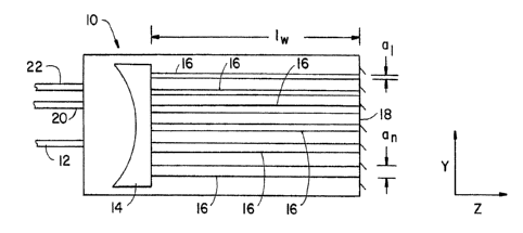
FIG. 1 is a plan view of a new demultiplexing optic in planar form having a
plurality of parallel waveguides for dispersing different wavelength signals.

FIG. 2 is a graph showing phase front tilt to two different wavelengths
5 measured across a central passageway of the optic.

FIG. 3 is a graph showing an index profile superimposed on a section of
waveguide.

FIG. 4 is a plan view of a second demultiplexing device having a co,))",on
waveguide for dispersing different wavelength signals.

FIG. 5 is a cross-sectional end view of the common waveguide showing a
tapered core Isyer.

FIG. 6 is a cross-sectional end view of the common waveguide showing a
tapered cladding layer.

FIG. 7 is a plan view of a third demultiplexing device having a common
~5 waveguide with varying conce"lr~lions of dopant for dispersing dirrl3,~"~
wavelength signals.

FIG. 8 is a plan view of a fourth demultiplexing device having a plurality of
radial waveguides for dispersing different wavelength signals.

Detailed Descri,~,tion

Illustrated by drawing FIGS. 1-3 is a first embodiment of my invention
implemented in planar optics. The embodiment is described with respect to a

CA 02236970 1998-0~-07
W O 97/25639 PCT~US97/00077


direction of light travel for a demultiplexer but could function equally well in the
opposite direction of light travel as a multiplexer. In fact, the terms ~multiplexer"
and "demultiplexer" are used only for the purpose of referencing the embodiment
to one of these possible functions but do not exclude the other.

Optical signals of differing wavelengths (i.e., A, through An) enter a planar
demultiplexing optic 10 from an input waveguide (or optical fiber) 12 and diverge
to fill the aperture of a focusing optic (collimating lens) 14. The diverging
wavefronts are collimated by the focusing optic 14. Discrete portions of the
wavefronts propagate through a plurality of parallel waveguides 16 to a flat
reflective optic 18, which retrorerlects the wavefronts on a return path to the
focusing optic 14. The input waveguide 12 is preferably located along an opticalaxis of the focusing optic 14, but similar principles also apply for off-axis
arrangements.

The parallel waveguides 16, which form a central pathway through the planar
optic 10, share a common length ''Iw'' in a direction "Z" of wavefront propagation
but progressively vary in width from "a1" to "ann along orthogonally related
direction u~,. The change in waveguide width from "a," to ~an" indirectly variesoptical path lengths UL;" of the different waveguides 16 by changing an effective
refractive index "n&~F" according to the following relationship:

Li=neff-~

The change in optical path lengths "Lj" evaluated at the reflective optic 18
relatively inclines the waver, ~ Ls according to their wavelengths A, - An as shown
in the graph of FIG. 2. The graph ordinate spans the waveguides 16 in the
direction "~' at a position coincident with the reflective optic 18. The graph
25 abscissa is in units of phase angle "q)". The stepped line (p(A,) represents a
collection of the phase angles ~ n in the waveguides 16 for the wavelength A,.

CA 02236970 1998-0~-07

W O 97/25639 PCT~US97/00077


The stepped line l~p(An) represents a collection of the phase angles "q)" in thewaveguides 16 for the wavelength An. The angular difference between the two
stepped lines ~(A,) and (p(An) represents a difference in phase front tilt between
the two wavelengths A, and An~

The phase front tilt changes the focus of the returning waverl onls from
coincidence with the input waveguide 12 (the expected focus of retroreflected
waver. . "ts that are not tilted) to output waveguides 20 and 22 according to the
respective amounts of tilt. For example, the wavelength A, focuses on the closeroutput waveguide 20 and the wavelength An focuses on the more distant output
waveguide 22. Of course, more wavelengths A between the wavelengths A, and
Anl representing additionai signals (or channels), could be focused on additional
output waveguides positioned between the waveguides 20 and 22. The number
of waveguides 16 could be increased to more accurately image the mode field of
the input waveguide 12 on each of the output waveguides 20 and 22.

The effective index Und," of the respective waveguides is a quotier~t of
propagation constant ~ " and wave numberUkO~ as follows:


neff = -


where the wave number ~ can be expressed in terms of wavelength as
follows:
2~
ko =--


CA 02236970 1998-0~-07

W O 97/25639 PCTAUS97/00077


The propagation constant ",13" can be calculated from a wave equation using
well-known techniques. An example of a wave equation for a planar optical
waveguide found in a reference by J. P. Meunier et al., Optical and Quantum
Electronics 1~, (1983) 77-85, is as follows:

d +k2 n2 (x) (Pm (x) = l~m ~Pm (x)


where the term "~pm(x)n is a field distribution of the mode and Un(x)" is the
index profile of the core. The index profile "n(x)", which is shown in the cross-
sectional view of FIG. 3, depends on the profile shape, core dimension "a", and
the peak index values Un0'' of core 24 and "nC,adr of cladding 26. The latter peak
10 index values "nO" and Unclad" are often considered together as the variable u~",
which is defined as follows:
~ nO--nclad
nO


Any of these variables that affect the index profile Un(x)n of the respective
waveguides 16 also can be used to change the propagation constant U,B", which
5 in turn changes the effective index "nOff" and the resulting optical path length ULjD
of the waveguides 16. The progressive variation in optical path length "Lj" of the
waveguides 16 in the U~' direction produces the different wavefront tilts of thewavelength A, and Anl causing them to focus in the different positions occupied
by the output waveguides 20 and 22.

CA 02236970 1998-0~-07

W O 97/25639 PCT~US97/00077


Preferably, the profile shape of non-step index waveguide profiles Is adjusted
so that changes in the waveguide dimensions, e.g., "a", or changes in the peak
indices, e.g., "~\", produce larger changes in the propagation constant U~ This
limits the amount of required physical change between the different waveguides
s 16. Also, the waveguides are preferably single mode to better control
differences between their optical path lengths ~Ljn.

Two versions of a second embodiment of my invention are illustrated in FIGS.
4-6. A new planar demultiplexing optic 30 includes several of the same
components as the planar optic 10 including input waveguide 32, collimating
0 optic 34, reflecting optic 38t and output waveguides 40 and 42. However, theplurality of individual waveguides 16 are replaced by a common waveguide 36.
Instead of varying respective width dimensions Ua,n through "an~ of individual
waveguides, a thickness dimension utn of the common waveguide 36, which is
measured in a direction "X", is varied in the same "Y" direction transverse to the
direction UZn of wavefront propagation.

The common waveguide 36 is formed by a continuous layer 44 of core
material located between continuous layers 46a and 46b of cladding material on
a planar substrate 48. In one version of this embodiment, illustrated by FIG. 5,the core layer 44 continuously varies in thickness from ut"1n to ~t~2n across the
20 comrllon waveguide 36. In the other version, iltustrated by FIG. 6, the cladding
layer 46a varies in thickness from utbln to "tb2" across the common waveguide 36.

Both thickness variations result in a continuous change of the propagation
cc~)slanl U13n in the I~Yn direction across the waveguide. The collimating optic 34
limits any movement of the propagating waver, onls in the "Y" direction, so
individual waveguides are not required to separate the propagating waver, un L~
into separate paths having different optical path lengths U~jD, The continuous
variation of the propagation constant U~3n iS expected to more accurately project
the mode field of the input waveguide 32 on each of the output waveguides 40


,

CA 02236970 l998-0~-07

W O 97n5639 PCT~US97/00077


and 42.

The planar multiplexing optics 10 and 30 are particularly suitable for
simpllfled manufacture by "redraw" in which layers of core 44 and cladding 46a
and 46b are deposited on the substrate 48 with additional thickness and a~e
5 stretched together with the substrate to exact dimensions. The process permitsmuch wider tolerances for deposition. Alternatively, grinding or polishing couldbe used to control waveguide thickness.

A third embodiment of my invention, illustrated in FIG. 7, includes several
features in common with the second embodiment. A planar demultiplexing optic
50 includes an input waveguide 52, a focusing optic (collimating lens) 54, a
common waveguide 56, a flat reflective optic 58, and output waveguides 60 and
62. In contrast to the second embodiment, the propagation constant "~3" is varied
by a change of rer,a~;live index across the common waveguide 56. For example,
either or both of the peak refractive indices of the core 64 and cladding 66 can15 be changed, such as by adding varying concenl,aLions of dopant 68. The result,
however, is similar to the second embodiment, namely, a continuous variation in
the optical path length in the uy7~ direction.

The change in rer, active index can be made in several ways including using a
thin film approach such as OVD (outside vapor deposition) and PECVD (plasn~a-
20 enhanced chemical vapor deposition). The varying concentrations of dopant 68could also be achieved using ion exchange techniques.

A fourth and final embodiment shown in FIG. 8 is formed as a planar
demultiplexing optic 70 including an input waveguide 72 and a focusing optic 74,which has zero power but provides a free-space region for converyil ,9 or
25 diverging wavefronts. A periodic array of radial waveguides 76, which form a
central pathway through the optic 70, terminate at a curved reflective optic 78.Each radial waveguide 76 conveys a separate portion of a respective cylindrical

CA 02236970 1998-0~-07
W O 97/25639 PCTrUS97/00077


wavefront corresponding to one of the wavelengths "A1" through UAn". The curved
reflective optic 78 retroreflects the cylindrical wavefronts on a converging path
through the radial waveguides 76 to the free-space of the focusing optic 74.
J


However, similar to the first embodiment, the radial waveguides 76
5 progressively vary in width from ~alU to "an" for changing the propagation
constant "~3" of different portions of the cylindrical wavefronts. Although the
waver~o"ls of the different wavelengths "A,'' through ~An~ propagate cylindrically,
the change in propagation constant "~" remains transverse to the instant
directions of wavefront propagation along the radial waveguides 76. The
0 resulting change in the optical path lengths "~," of the radial waveguides 76
relatively inclines the cylindrical wavefronts of the different wavelengths ~A,"through UAn", causing them to converge to slightly different focus positions at
output waveguides 80 and 82.

Although the above-described embodiments of my invention are implemented
5 in planar optics, bulk or hybrid implementations are also possible. For example,
optical fibers could be substituted for the parallel waveguides 16 of optic 10 or
the radial waveguides 76 of optic 7Q. The various means for changing
propagation constants disclosed in any one of the embodiments could also be
applied to other of the embodiments. For example, the individual waveguides of
2~ FIGS. 1 and 8 could also be varied in thickness or in various refractive qualities.
Combinations of the various means for chanyil ,g the propagation CGI ,:,la"l, aswell as transverse variations in the length ''Iw~, could be used for further tuning
the input and output mode fields.

The waveguides in the illustrated embodiments have been depicted as buried
25 waveguides, but other known types of waveguides including rib waveguides
could also be used. Similarly, the focusing optic, which has been depicted as a
lens, could also be arranged together with the input or output waveguides as a
mirror, such as a collimating mirror or similar reflective surface. The input and

CA 02236970 l998-05-07

W O 97125639 PCT~US97/00077
12

output waveguides of the various embodiments could also be arrayed in various
combinations including equal numbers of input and output waveguides.

Representative Drawing
A single figure which represents the drawing illustrating the invention.
Administrative Status

For a clearer understanding of the status of the application/patent presented on this page, the site Disclaimer , as well as the definitions for Patent , Administrative Status , Maintenance Fee  and Payment History  should be consulted.

Administrative Status

Title Date
Forecasted Issue Date 2002-12-03
(86) PCT Filing Date 1997-01-06
(87) PCT Publication Date 1997-07-17
(85) National Entry 1998-05-07
Examination Requested 2001-11-19
(45) Issued 2002-12-03
Deemed Expired 2004-01-06

Abandonment History

There is no abandonment history.

Payment History

Fee Type Anniversary Year Due Date Amount Paid Paid Date
Registration of a document - section 124 $100.00 1998-05-07
Application Fee $300.00 1998-05-07
Maintenance Fee - Application - New Act 2 1999-01-06 $100.00 1998-12-22
Maintenance Fee - Application - New Act 3 2000-01-06 $100.00 1999-12-14
Maintenance Fee - Application - New Act 4 2001-01-08 $100.00 2001-01-03
Request for Examination $400.00 2001-11-19
Maintenance Fee - Application - New Act 5 2002-01-07 $150.00 2001-12-27
Final Fee $300.00 2002-09-16
Owners on Record

Note: Records showing the ownership history in alphabetical order.

Current Owners on Record
CORNING INCORPORATED
Past Owners on Record
BHAGAVATULA, VENKATA A.
Past Owners that do not appear in the "Owners on Record" listing will appear in other documentation within the application.
Documents

To view selected files, please enter reCAPTCHA code :


To view images, click a link in the Document Description column. To download the documents, select one or more checkboxes in the first column and then click the "Download Selected in PDF format (Zip Archive)" or the "Download Selected as Single PDF" button.

List of published and non-published patent-specific documents on the CPD .

If you have any difficulty accessing content, you can call the Client Service Centre at 1-866-997-1936 or send them an e-mail at CIPO Client Service Centre.


Document
Description 
Date
(yyyy-mm-dd) 
Number of pages   Size of Image (KB) 
Abstract 1998-05-07 1 44
Description 1998-05-07 12 476
Cover Page 1998-08-17 1 33
Claims 1998-05-07 10 376
Drawings 1998-05-07 3 43
Cover Page 2002-10-31 1 38
Representative Drawing 2002-04-08 1 9
Correspondence 2002-09-16 1 33
Assignment 1998-05-07 3 110
PCT 1998-05-07 8 252
Correspondence 1998-07-28 1 30
Prosecution-Amendment 2001-11-19 1 26
Prosecution-Amendment 2002-02-19 1 38
Assignment 1998-07-31 1 21
Assignment 1998-07-16 3 107