Note: Descriptions are shown in the official language in which they were submitted.
CA 02237619 1998-OS-O1
WO 98!10511 PCTliJS97/14763
FREQUENCY CONVERSION CIRCUIT AND METHOD FOR MILLIMETER
WAVE RADIO
DACKGROUND OF THE. INVENTION
Field of the InvE:ntion
This invention relates to frequency conversion that
employs a combination of frequency mixing and multipli
cation for conversion between a low frequency modulation
signal and a radio frequency (RF) signal in the millime-
ter wave range using a low frequency synthesizer.
Description of tree Related Art
Millimeter wave radios require conversion of lower-
frequency baseband modulation signals to millimeter wave
radio frequency (RF) signals fox transmission. A
baseband modulation signal modulates an intermediate
frequency (IF) wave by mixing the modulation signal with
the IF wave from a local oscillator to produce a modu-
lated IF signal, the frequency of which is the sum of
the baseband frequency and the local oscillator's fre-
quency.
There are two major conventional schemes to convert
an IF signal to a millimeter wave RF signal for radio
transmission. The first scheme involves direct mufti-
plication of the frequency of the modulated IF signal to
a millimeter wave frequency, as shown in FIG. 1. A mod-
' ulating signal :Z at a low baseband frequency fmod is
mixed with an IF wave 4 at a frequency fl in a mixer 6,
which produces an upconverted modulated signal 8 at an
intermediate frequency fIF equal to the sum of fmod and fl.
CA 02237619 1998-OS-O1
WO 98/lOSll PCT/US97/i4763
2
The IF signal is then fed into a frequency multiplier 10
which increases the frequency of the IF signal by multi-
plying f=F by N, resulting in an RF signal 12 at a milli-
meter wave frequency fRF. This scheme of direct f requen-
cy multiplication is described in Patent No. 5,495,255 ,
for a frequency modulation (FM) radar system.
A major disadvantage of the direct frequency multi-
plication scheme in FIG. 1 for a millimeter wave radio
is that the frequency multiplier 10 introduces
nonlinearities when the modulated IF signal is multi-
plied by N, resulting in an RF signal l2 that has a dis-
torted signal shape compared to the modulation signal.
Direct multiplication is suitable for modulation schemes
that are not amplitude sensitive, such as FM or frequen-
cy shift keying (FSK). However, direct multiplication
is not suitable for modulation schemes that require
linearity, such as amplitude modulation (AM) or high
level quadrature amplitude modulation {QAM).
Another conventional scheme to produce an RF signal
in-the millimeter wave range is to use a millimeter wave
synthesizer, as shown in FIG. 2. A baseband modulation
signal 14 at a frequency fmod is mixed with an IF wave 16
at a frequency f~~in a mixer 18 to produce a modulated IF
signal 20 at a frequency f=F. The IF signal 20 is then
mixed with a millimeter wave 22 generated by a millime
ter wave frequency synthesizer 24 in a high frequency
mixer 26, which produces a modulated millimeter wave
signal 28 at a frequency fRF. This scheme is described
in Patent No. 5,428,668 for lower RF frequency cellular
telephone applications.
The millimeter wave frequency synthesizer 24 in '
FIG. 2 is very expensive due to hardware complexity re-
quired f or synthesizing millimeter wave frequencies di- '
rectly. Moreover, a millimeter wave frequency synthe-
sizer has a limited tuning bandwidth, and therefore is
not suitable for wide bandwidth radios. If a multiple
CA 02237619 2000-07-26
3
number of millimeter wave frequency synthesizers are used
to cover a desired tuning bandwidth, the radio would be
even more costly.
SUMMARY OF THE INVENTION
The present invention provides a frequency
conversation circuit and method for converting a baseband
modulation signal to a millimeter wave radio frequency
(RF) signal and vice versa, using a low frequency
synthesizer, a plurality of frequency multipliers, and a
plurality of mixers.
In the radio transmitter, a modulated signal is
first mixed with the synthesizer frequency of a low
frequency synthesizer to produce a modulated synthesizer
frequency. The synthesizer frequency is also multiplied
in a cascade of frequency multipliers in a path parallel
to the modulated synthesizer frequency signal to convert
the synthesizer frequency to a millimeter wave frequency.
This millimeter wave frequency is then mixed with the
modulated synthesizer frequency to produce a modulated
millimeter wave RF signal for transmission.
The radio receiver performs the reverse operation.
A received RF signal is mixed with the multiplied
synthesizer frequency and thereby downconverted to a
lower modulated synthesizer frequency for reception.
Accordingly, in one aspect of the present invention
there is provided a signal conversion circuit for
simultaneously converting a transmit baseband signal to a
transmit signal and converting a receive signal to a
receive baseband signal, comprising:
a transmit frequency-conversion circuit and a
receive frequency-conversion circuit that each include:
CA 02237619 2000-07-26
3a
a) first, second and third mixers that are
serially connected with said second mixer positioned
between said first and third mixers;
b) a frequency synthesizer connected to said
second mixer; and
c) at least one frequency multiplier connected
between said frequency synthesizer and said third mixer;
a local oscillator connected between the first mixer
of said transmit frequency-conversion circuit and the
first mixer of said receive frequency-conversion circuit;
a transmit baseband signal that is coupled to the
first mixer of said transmit frequency-conversion circuit
being converted into said transmit signal at that
circuit's third mixer; and
a receive signal that is coupled to the third mixer
of said receive frequency-conversion circuit being
converted into said receive baseband signal at that
circuit's first mixer.
According to another aspect of the present invention
there is provided a method for simultaneously converting
a transmit baseband signal to a transmit signal and a
receive signal to a receive baseband signal, comprising
the steps of:
generating a local oscillator signal;
providing a frequency-conversion process that
includes the processes of:
a) generating a converter signal;
b) multiplying said converter signal to
generate a multiplied converter signal; and
c) mixing an input signal with said local
oscillator signal, said converter signal and said
CA 02237619 2000-07-26
3b
multiplied converter signal to generate a frequency-
converted signal;
applying said frequency-conversion process to said
transmit baseband signal wherein said input signal is
said transmit baseband signal and said frequency-
converted signal is said transmit signal; and
simultaneously applying said frequency-conversion
process to said receive signal wherein said input signal
is said receive signal and said frequency-converted
signal is said receive baseband signal.
This invention has two distinct characteristics that
make it attractive for low cost commercial radios.
First, the modulated signal is not frequency multiplied
in any circuit path, thereby avoiding nonlinearities in
the signal that would otherwise be introduced by
frequency multipliers. Because this frequency conversion
circuit basically preserves signal linearity, it can be
used for a variety of modulated formats such as FM, AM
and QAM.
CA 02237619 1998-OS-O1
WO 98/10511 PCT/US97/14763
4
A second advantage is that a low frequency synthe-
sizer can be used, thus greatly reducing the circuit's
cost. Because the tuning bandwidth of the low frequency
synthesizer is multiplied by the composite multiplica-
tion factor of the cascaded frequency multipliers, a
wide RF tuning bandwidth can be achieved with relatively
narrow synthesizer tuning bandwidth. Therefore, one
synthesizer in the frequency conversion circuit can cov
er the radio's full bandwidth, further reducing the cir
cuit's cost.
These and other features and advantages of -the in-
vention will be apparent to those skilled in the art
from the following detailed description, taken together
with the accompanying drawings, in which:
BRIEF DESCRIPTION OF THE DRAWII~TGS
FIG. 1, described above, is a schematic diagram of
a conventional millimeter wave radio transmitter using
direct multiplication of an IF signal to generate an RF
signal;
FIG. 2, described above, is a schematic diagram of
a conventional millimeter wave radio transmitter using a
millimeter wave frequency synthesizer;
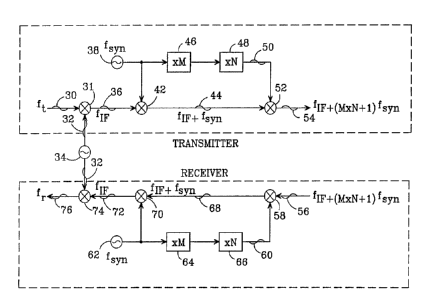
FIG. 3 is a schematic diagram of a millimeter wave
radio transmitter and receiver in accordance with the
invention that employ a combination of frequency multi
plication and mixing using a low frequency synthesizer..
DETAILED DESCRIPTION OF THE INVENTION
The present invention provides a frequency conver-
sion circuit for a millimeter wave radio transmitter and
receiver. The circuit concerns the use of a low fre-
quency synthesizer and a combination of cascaded fre-
quency multipliers and mixers to achieve conversion from
a modulation signal to a millimeter wave RF signal for
transmission, and vice versa for reception.
CA 02237619 1998-OS-O1
WO 98/10511 PCTlLTS97/14763
FIG. 3 is a schematic diagram of a preferred em-
bodiment of the invention. The transmitter and receiver
circuits are ba:~ically symmetrical. If the transmitter
and receiver circuits are implemented in a single radio,
5 identical mixer and multiplier components for come-
sponding functions may be used for both the transmitter
and the receiver to simplify manufacture.
In the transmitter, a baseband modulation signal 30
at a frequency ft is mixed in a mixer 31 with an interme-
diate frequency (IF) wave 32 generated by a local oscil-
lator 34 at a frequency fl to produce an IF signal 36 at
a frequency f=F, which is the sum of ft and fl. The
baseband modulation signal is preferably in the frequen-
cy range of 50-500 MHz. Although it is possible to con-
vert a baseband modulation signal to an RF signal with-
out the use of IF, it is preferred that the baseband
modulation signal be converted to an IF signal first to
allow for a wide tuning range if the baseband signal has
a wide bandwidth. The local oscillator frequency fl is
preferably much higher than the baseband frequency ft,
and is preferably in the range of 500 MHz to 3 GHz. It
is further preferred that the IF frequency be approxi-
mately five times the baseband frequency of the modula-
tion signal, so that the baseband modulation frequency
is much smaller than the IF to allow for easy filtering
and tuning. For example, if the frequency of the
baseband modulation signal is 300 MHz, the IF frequency
is preferably 1.5 GHz. The transmitter employs a low
frequency synthesizer 38 that provides a synthesizer
frequency fa~,r" preferably in the range of 1-5 GHz. For
' example, if a desired millimeter wave RF is about 40
GHz, and a desired composite multiplication factor is
' 10, then the synthesizer frequency f$I,I, should be about
4
GHz. The synthesizer frequency is mixed with the IF
signal 36 in a mixer 42 to produce a signal 44 at a fre-
quency that is the sum of fIF and faa,I,. In another path,
CA 02237619 1998-OS-O1
WO 98/10511 PCT/US97/14763
6
the synthesizer frequency is multiplied in a xM frequen-
cy multiplier 46 and a xN frequency multiplier 48 that
are cascaded together to generate a multiplied frequency
50 that is MxNxfe},I" where M and N axe positive integers.
Preferably, the multiplication factors M and N are each
no more than 5 to avoid excessive degradation in phase
noise. It is further preferred that the multiplication
factor in each of the multipliers equal 3, so that a
frequency that is 9 times f81", is generated. The multi-
plied frequency 50 is then mixed with~'the fif+fs~ signal
44 in a mixer 52 to generate a millimeter wave RF signal
54 at a frequency of f=F+ (MxN+1 ) xfsm. The RF signal
preferably has a frequency range of 30-90 GHz. ~ If each
of the frequency multipliers has a preferred multiplica-
25 tion factor of 3, then the IF signal is upconverted to
an RF signal by 10 times the synthesizer frequency.
This multiplication factor is a good compromise between
hardware complexity and phase noise degradation result-
ing from the multiplication.
There are several distinct advantages of this cir-
cuit. First, the modulation signal ft is upconverted in
frequency only by mixing in mixers 31, 42, and 52, and
is not frequency multiplied in any circuit path, thus
avoiding nonlinearities,associated with frequency multi-
pliers that cause distortion to the modulation signal.
Because this frequency conversion circuit preserves sig-
nal linearity, it is suitable for various types of modu-
lation such as FM, FSK, AM and QAM. Second, a low fre-
quency synthesizer 38 with fs~, in 1-5 GHz range can be
used, which is much less expensive than a millimeter
wave frequency synthesizer. Moreover, the tuning band-
width of the frequency synthesizer 38 is multiplied by
the composite multiplication factor of the cascaded fre-
quency multipliers 46 and 48, resulting in a wide RF
tuning bandwidth for the RF signal 54. Therefore, only
one inexpensive low frequency synthesizer is needed to
CA 02237619 1998-OS-O1
WO 98/10511 PCT/L1S97/14763
7
cover the radio's full tuning bandwidth.
In another embodiment, one frequency multiplier can
be used instead of two cascaded multipliers 46 and 48.
However, the multiplication factor would be limited with
a single multiplier because phase noise degradation
would become excessive with a multiplication factor that
is greater than 5. Therefore, the synthesizer frequency
f8n, would have to be much higher, thus increasing the
circuit's cost.
The frequency conversion circuit for the radio re-
ceiver is preferably the same as that of the transmitter
except that the: operation is reversed. A received RF
signal 56 at a frequency fIF+ (MxN+1 ) f$}"z is downconverted
in frequency by a mixer 58, which mixes the incoming RF
signal 56 with a multiplied synthesizer frequency wave
60 resulting from a synthesizer 62' s frequency fBs,I, being
multiplied in a cascade of multipliers 64 and 66. The
downconverted signal 68 is then mixed with synthesizer
frequency fs~ in a mixer 70 to be further downconverted
to an IF signal 72 at the frequency fIF. The IF signal
72 is then mixed with the IF wave 32 from the local os-
cillator 34 in a mixer 74 to produce a baseband modula-
tion signal 76 having a baseband frequency fr. In a mil-
limeter wave radio, one IF local oscillator 34 may be
used for both transmission and reception using the same
IF frequency. Moreover, the transmitter's and the re-
ceiver's frequency conversion circuits may use identical
mixer and multiplier components for corresponding func-
tions, thus further reducing the cost of manufacturing.
If the transmitter and the receiver are remote from each
' other, separate local oscillators would need to be pro-
vided for both.
The advantages of the transmitter frequency conver-
sion circuit described above also apply to the receiver
circuit. The advantages include low signal distortion,
low phase noise degradation, wide tuning bandwidth, and
CA 02237619 1998-OS-O1
WO 98/lOSlI PCT/LFS97/14763
8
use of an inexpensive low frequency synthesizer.
While several illustrative embodiments of the in-
vention have been shown and described, numerous varia-
tions and alternate embodiments will occur to those
skilled in the art. Such variations and alternate em- ,
bodiments are contemplated, and can be made without de-
parting from the spirit and scope of the invention as
defined in the appended claims.