Note: Descriptions are shown in the official language in which they were submitted.
CA 02237677 1998-OS-14
PRINTED WIRING BOARD
BACKGROUND OF THE INVENTION
1. Field of the Invention:
!', The present invention relates to a printed-wiring
board, more particularly to a printed-wiring board
comprising at least one electronic circuit and a
substrate having two or more conductor layers for
mounting said at least one electronic circuit.
l() 2. Description of the Prior Art:
It is well known that a printed-wiring board
mount~ad with a circuit element such as a transistor,
an IC or an LSI often generates an electromagnetic
noise, and hence a failure is sometimes caused in an
:LO electronic apparatus itself which has the built-in
print.=_d-wiring board or in other related electronic
apparatus.
Among causes which generate the failure of the
electronic apparatus of this like, the cause of
a,() particular large weight is a conductive or a
radioactive electromagnetic wave produced by a current
(a sneak current) which flows through the parasitic
capacity or the parasitic mutual inductance of a
circuit, called a common mode phenomenon. Since the
to generation mechanism of the electromagnetic wave of
this l~cind is complex, an effective countermeasure near
CA 02237677 1998-OS-14
the failure generation source which is considered most
effective has not been established. Therefore, a
conventional countermeasure has been to control the
conduction or the radiation of the electromagnetic
wave by electromagnetically shielding the whole
electronic apparatus with a metallic cover and
providing a common-mode choke coil or core for the
cable outwardly extending from the apparatus. On the
other hand, with reference to the printed-wiring board
1() of the conventional type, as shown in Fig. 2, high
frequency capacitors C1 - Cn are often connected
between power supply terminals 3a - 3n and ground
terminals 4a - 4n of electronic circuits Z1 - Zn such
as the IC, LSI (hereinafter simply called an
electronic circuit) connected respectively to power
supply line 1 which corresponds to power source
condu~~tor layer 1 and grounding line 2 which
corresponds to ground conductor layer 2 of the
print~ad-wiring board. The purpose of this arrangement
a?U is to flow the high frequency current, which flows in
power supply line 1 accompanying the high frequency
operation of electronic circuits Z1 - Zn, in high
frequency capacitors C1 - Cn to decrease (that is,
filtering) the high frequency fluctuation of the power
to sourcE~ terminal voltage and to restrict the coupling
(that is, decoupling) with other electronic circuit
z
CA 02237677 2001-05-16
74570-66
sharing power supply line 1. However, in particular, for
effectively reducing the fluctuation of the power supply
voltage, the conventional printed-wiring board is structured,
as shown in Fig. l, with power source conductor layer 1 made of
all flat plate having no wiring in order to lower the impedance
of the power supply line. The conventional printed-wiring
board is structured, as ~~hown in Fig. 1, with insulative board
layers 6, which are, e.c~., typical resin substrates.
The above conventional printed-wiring board has a
problem that a circuit designer cannot control the high
frequency current which flows in the power supply line
accompanying the high frequency operation of said electronic
circuit.
In other wordy>, when the power conductor layer is
made of a flat plate over the whole area without having wiring,
the impedance of the power supply line is small, and hence even
if a high frequency capacitor is connected between the power
source terminal and the ground terminal of the electronic
circuit, it is hard to control the high frequency power source
current which flows out to the power supply line, and
resultantly the high frequency power source current flows in
the decoupling capacitor disposed in the vicinity of other
electronic circuits which share the power supply line.
Therefore, the analysis of the high frequency power source
current with reference t.o the whole printed-wiring board is
very difficult and
3
CA 02237677 1998-OS-14
hence it is unable to strictly select the decoupling
capacitor to be used for each electronic circuit.
Further, the distribution of the high frequency
power source current on the whole printed-wiring board
o is ve=ry complex. Depending on the arrangement of
elect=ronic circuits on the printed-wiring board or on
the operation state of the electronic circuits even if
they are in the same arrangement, the high frequency
power source current distributes in such a manner to
1() form a large loop, having the probability of
introducing the problem of electromagnetic radiation
or immunity.
For example, as shown in Fig. 2, electronic
circuits Zl (a large current), Z2 (a medium current)
to and Zn (a small current) for different high frequency
power source currents are connected respectively to
both power supply line 1 and ground line 2. Mainly
from t:he mounting and 1=he cost restrictions,
capacitors C1, C2 and (.n of capacitance corresponding
2~) to respective high frequency power source currents
(large capacitance for Z1, medium capacitance for Z2,
small capacitance for Z3) are connected to respective
electronic circuits. When the electronic circuits on
the printed-wiring board operate in this state, since
capacitor Cn of small capacitance, connected between
the power source terminal and the ground terminal of
CA 02237677 2001-05-16
74570-66
electronic circuit Zn fo:r small high frequency power source
current, has the impedance larger than that of other
capacitors, the high frequency power source current of
electronic circuit Zn f:L~~ws into capacitor C2 of medium
capacitance (having srnal:l impedance compared to that of Zn)
connected between the power source terminal and a ground
terminal of electronic circuit Z2 for a medium high frequency
power source current, or into capacitor C1 of large capacitance
connected between the power source terminal and the ground
terminal of electronic circuit Z1 for a large high frequency
power source current. Further, if the capacitors are of-_ the
same type, the frequency characteristic of the impedance
becomes different according to each capacitance, and the
impedance of the capacitor of small capacitance tends to become
smaller than the impedance of the capacitor having the larger
capacitance, in the region where the number of the high
frequency exceeds some value. Therefore, when viewed in the
broad frequency band, electric currents flow to and fro in a
complicated way between electronic circuits on the printed-
wiring board. As a reslz_Lt, the loop made by the high frequency
power source current becomes large or the high frequency
current of the common mode is made to flow into such as the
cable connected from onE=_ printed-wiring board to
5
CA 02237677 1998-OS-14
another printed-wiring board, thereby increasing the
conductive or radioactive electromagnetic waves.
These phenomena have caused the electromagnetic
interference between the electronic apparatus, that is,
EMC problem. Further, for example, high frequency
power source voltage fluctuation with reference to one
electronic circuit on the printed-wiring board
sometimes becomes an issue. In this case, even if the
capacitance of a decoupling capacitor in the vicinity
I() of the electronic circuit is increased, it is not
effective because the more the capacitance is
increased, the more the high frequency power source
currents of other electronic circuits flow into the
circuit, and consequently it becomes hard to decrease
l~~ the high frequency power source voltage fluctuation
with 'the probability of failing in securing the high
frequ<~ncy operation of the electronic circuit.
Further, when the latest IC/LSI is used in a
logical unit which operates at a low frequency, for
2U preventing the generation of the unnecessary
conductive or radioactive electromagnetic waves to be
caused due to excessiv<~ly fast rise time or fall time
of a rectangular wave signal of the IC/LSI, sometimes
a high frequency filter is inserted in the circuit to
2o slow t:he rise time and the fall time of the
rectangular wave signal of the IC/LSI. However, when
CA 02237677 1998-OS-14
the high frequency filter of this like is newly added
as parts, the high density mounting efficiency on the
printed-wiring board is disadvantageously affected.
Therefore, with the conventional printed-wiring
board, it becomes necessary to electromagnetically
shiel~~ the whole electronic apparatus with metal foil,
as described above, to protect against the EMC problem
and c~~ncurrently control the conduction of the
electromagnetic waves by attaching a common-mode choke
1() coil or core for the cable extending outwardly of the
apparatus. Still further, with reference to the
problE~m which hinders the high frequency operation of
the Ic~/LSI, it is necessary to meet the problem by
mounting capacitors of a required number or more on
lr~ the printed-wiring board to control the high frequency
power source voltage fluctuation of the whole wiring
board"
SUMMARY OF THE INVENTION
~() An object of the present invention is to provide
a printed-wiring board which can remarkably reduce the
generation of an electromagnetic noise, largely
increase the resistance to an extraneous
electromagnetic noise, and allows the smooth high
25 frequency operation of electronic circuits such as an
IC, LSI to be mounted.
7
CA 02237677 2001-05-16
74570-66
Another object: of the present invention is to provide
a printed-wiring board f=or which a circuit designer can control
the high frequency power- source current of each electronic
circuit such as an IC/L~~I mounted on the wiring board.
The printed-wiring board of the present invention
comprises at least one e-wectronic circuit and a substrate for
mounting the electronic circuit. The substrate comprises two
or more conductor layer~~ and a spiral coil inductor.
A plurality of: conductors are formed by cutting a
part of two conductor layers disposed opposite to each other
from among the conductor layers. The spiral coil inductor is
composed of this plurality of conductors and viaholes
vertically connecting between said plurality of conductors.
Further, on a part or the whole area between two conductor
layers disposed facing each other for composing the spiral coil
inductor, an insulative magnetic material is disposed in
layers.
It is allowable to use a structure such that a
capacitor is connected between a power supply side terminal and
a ground side terminal of: the electronic circuit, one end of
the spiral coil inductor is connected to the power source
terminal of the electronic circuit and the other end thereof is
connected to the power e;ource conductor layer. In this case,
the spiral coil inductor constitutes a structural element of a
decoupling circuit while discharging a large decoupling
function with a small s~>ace.
It is allowable to use a structure such that a high
frequency filter is connected between an output terminal of one
electronic circuit and an input terminal of another electronic
circuit, the .high frequency filter including the spiral coil
inductor as a structural element thereof. In this case, when
8
CA 02237677 2001-05-16
74570-66
the latest IC/LSI is usE:d as the electronic circuit which
operates at a low frequency, even if the rise time or the fall
time of a rectangular wave signal of the IC/LSI is too fast,
unnecessary conductive or radioactive electromagnetic waves are
not generated.
A part of the ground conductor layer and the power
source conductor layer disposed opposite to each other may be
used as two layers of conductor layers which constitute a
spiral coil inductor. I:n this case, the spiral coil inductor
is sometimes composed without using the additional number of
conductor layers compared with the conventional case.
Two layers of conductor layers used for composing the
spiral coil inductor arE°. each a part of the power source
conductor layer and can have at least one layer of a ground
layer outside of two conductor layers. In this case,
unnecessary conductive c>r radioactive electromagnetic waves are
not generated and the distortion of the signal waveform becomes
minimum.
Furthermore, i.t may take a structure having a viahole
vertically connecting between two signal conductor layers while
penetrating two conductc>r layers, and having another viahole
connected to two ground conductor layers at both ends thereof
being disposed in the proximity of the viahole. Also in this
case unnecessary electromagnetic waves are not generated and
the signal waveform distortion becomes minimum.
As an insulati.ve magnetic material, a mixture of a
ferrite fine powder of one of an Ni-Zn group, a Mn-Zn group,
Sendust or a Li group arid an insulative solvent may be used.
Also as the insulative scolvent, epoxy group insulative solvent
can be used.
9
CA 02237677 2001-05-16
74570-66
Further, the insulative magnetic material can be
formed of a plurality of. magnetic films, with insulation
coating on both sides of. the insulative magnetic material. It
is also possible to use a multilayer band of amorphous magnetic
film as the plurality of: magnetic films.
In accordance with the present invention, there is
provided a printed-wiring board comprising: at least one
electronic circuit; and a substrate for mounting said
electronic circuit, wherein said substrate comprises: two or
more conductor layers; a coil inductor composed of a plurality
of conductor strips formed by cutting a part of a pair of
conductor layers disposed opposite to each other from among
said conductor layers, and viaholes connecting said plurality
of conductor strips; an insulative magnetic material being
disposed between said :pair of conductor layers facing each
other used for composing said coil inductor; and wherein a
first end of said coil inductor is connected to a power source
terminal of said electronic circuit and a second end of said
coil inductor is connected to a first power source conductor
layer.
The above and other objects, features and advantages
of the present invention will become apparent from the
following description with reference
CA 02237677 1998-OS-14
to the accompanying drawings which illustrate examples
of the present invention.
BRIEF DESCRIPTION OF THE DRAWING
o Fig. 1 is a longitudinal section of a
conventional example of a printed-wiring board,
F~'ig. 2 is a circuit diagram including electronic
circuits of the printed-wiring board of Fig. l,
Fig. 3 is a circuit symbol diagram of a spiral
1() coil inductor which constitutes a primary part of an
embodiment of the printed-wiring board of the present
invention,
F'ig. 4A is a plan view of a first embodiment of
the spiral coil inductor Ln of Fig. 3,
1~~ F'ig. 4B is a longitudinal section of Fig. 4A,
F'ig. 5 is a perspective view of the spiral coil
inductor Ln of Fig. 4A,
F'ig. 6A is a plan view of a second embodiment of
the spiral coil inductor Ln of Fig. 3,
~U Fig. 6B is a longitudinal section of Fig. 6A,
Fig. 7 is a circuit diagram showing an
application example of the spiral coil inductor of Fig.
3,
Fig. 8 is a perspective view of the spiral coil
'~5 induc for
of Fig. 3,
11
CA 02237677 1998-OS-14
Fig. 9 is a longitudinal section of a four-layer
printed-wiring board for constituting the spiral coil
inductor of Fig. 3,
Fig. 10 is a longitudinal section of a six-layer
o print~ad-wiring board for constituting the spiral coil
inductor of Fig. 3,
Fig. 11 is a longitudinal section of a six-layer
printed-wiring board different from that of Fig. 10
and used for constituting the spiral coil inductor of
Fig. 3,
Fig. 12 is a longitudinal section of a six-layer
printE~d-wiring board different from those of Fig. 10
and F:ig. 11 and used for constituting the spiral coil
induci~or of Fig. 3,
1~~ Fig. 13A is a graph showing measured results of
the radiation field intensity in a radio wave darkroom
with reference to the conventional example of the
printed-wiring board,
F.ig. 13B is a graph showing measurement results
similar to that of Fig. 13A prepared with reference to
the embodiment of the printed-wiring board of the
present invention,
Fig. 14A is another graph showing the measurement
result: of Fig. 13A,
F_Lg. 14B is an~othe.r graph showing the measurement
result: of Fig. 13B,
lZ
CA 02237677 1998-OS-14
Fig. 15A is a measurement chart showing the
magnetic field distribution in the vicinal area with
reference to the conventional example of the printed-
wiring board,
o F'ig. 15B is a measurement chart showing the
magnetic field distrif>ution in the vicinal area with
reference to the embodiment of the printed-wiring
board of the present invention,
Fig. 16 is a plan view showing the arrangement of
lU I/O connectors of the embodiment of the printed-wiring
board of the present invention,
Fig. 17 is a diagram showing a measuring system
for m~aasuring a common-mode current which parallelly
flows in an interface cable through the I/O connector.
to Fig. 18A is a graph showing the measurement
result of the common-mode current of I/0 connector
(RS23:2C1) of the conventional example of the printed-
wiring board,
Fig. 18B is a graph showing the measurement
2U resuli~ similar to that of Fig. 18A prepared with
referE~nce to the embodiment of the printed-wiring
board of the present invention,
F.ig. 19A is a graph showing the measurement
result. of the common-mode current of I/O connector
20 (RS23?.C2) of the conventional example of the printed-
wiring board,
13
CA 02237677 1998-OS-14
F'ig. 19B is a graph showing the measurement
result similar to that of Fig. 19A prepared with
reference to the embodiment of the printed-wiring
board of the present invention,
o Fig. 20A is a graph showing the measurement
result of the common-mode current of the I/O connector
(keyboard/mouse) of the conventional example of the
printed-wiring board,
Fig. 20B is a graph showing the measurement
IU result similar to that of Fig. 20A prepared with
refer.=nce to the embodiment of the printed-wiring
board of the present invention,
Fig. 21A is a graph showing the measurement
result of the common-mode current of the I/0 connector
~ (prinlter) of the conventional example of the printed-
wiring board,
Fig. 21B is a graph showing the measurement
resuli~ similar to that of Fig. 21A prepared with
reference to the embodiment of the printed-wiring
z0 board of the present invention.
DETAILED DESCRIPTION OF THE PREFERRED EMBODIMENTS
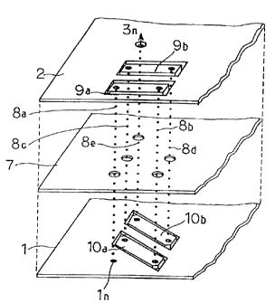
Fig. 3 shows circuit symbols of a spiral coil
inductor which is a primary part of a printed-wiring
25 board of the present invention, Fig. 4A and Fig. 4B
show a plan view and a section of the spiral coil
1 ~I
CA 02237677 1998-OS-14
inductor Ln of a first. embodiment of the printed-
wiring board of Fig. 3, respectively. Terminal
numbers In and 3n in the circuit symbols of Fig. 3
correspond to terminal numbers In and 3n of the plan
o view of Fig. 4A, respectively. In the first
embodiment of the printed-wiring board, a part of two
conductor layers 9, 10 disposed opposite to each other
are cut out to produce a plurality of conductor layers
9a, 9.b and 10a, lOb. In the whole region between two
condu~~tor layers 9a and 10a, 9b and lOb oppositely
disposed to each other, there are provided insulative
magnetic material 7 disposed in layers. By using
viaho.les 8a, 8b, 8c and 8d connecting between
conductor layers 9a and 10a, 9b and lOb, and
1~~ constr_ucting as shown in perspective views of Fig. 4A,
Fig. ~~B and Fig. 5, spiral coil inductors each being
an inductor of a spiral form are produced in the
printed-wiring board.
Figs. 6A and 6B show a plan view and a
2() longitudinal section o:E the spiral coil inductor Ln of
a second embodiment of the printed-wiring board of Fig.
3, respectively. In the printed-wiring board of the
second embodiment, as shown in Figs. 6A and 6B, the
structure is similar to that of the first embodiment
2o except. that insulative magnetic material 71 is
disposed in layers to f=orm the spiral coil inductor in
~ r~
CA 02237677 1998-OS-14
a partial region between two layers of conductors 9a
and 10a, 9b and lOb disposed facing each other.
I:n the printed-wiring board of the first and the
second embodiments, the spiral coil inductor is formed
!'~ by using two layers of_ conductor layers. The
inductance (L) of this coil is obtained in the
following equation.
L _ fy,usu''s1 henr ___ 1
( Y) ( )
1() where, ~cp: permeability in the vacuum (410-~),
~cS: relative magnetic permeability,
n: number of i~urns of spiral coil,
s: cross-sectional area of spiral coil (m2),
1: mean magnet=is path length of spiral coil
li (m),
From this equation, it is understood that the
inductance (L) is proportional to a square of the
number of turns of the spiral coil.
For example, in case of composing a
2() microstrip line in a well known meandering form, the
microstrip line may take a structure (J.P.A.
236488/1995) in which the insulative magnetic material
is di;~posed in layers on both sides of the conductor
layer which constitutes the microstrip line,
26 additionally providing ground conductor layers on both
1 (i
'CA 02237677 2001-05-16
74570-66
outsides of the magnetic material. However, in this case, the
electrostatic coupling between the microstrip conductor layer
and the neighbouring ground conductor layer functions to
control the impedance of the inductor. Therefore, even if the
conductor length of the inductor is lengthened, when the
wavelength of the current exceeds one half of the wavelength of
the problematic high frequency current, characteristic
impedance Zo of the transmission line on the lossless line is
given by equation (2). Specifically, Zo becomes the constant
inpedance which is independent of the length of the conductor
and the frequency of the>. applied current.
Zo = ~ ~cZ~ _
C
where, C: capacitance (F') between conductors oppositely
disposed, interposing a dielectric.
L: inductance (H) of the microstrip line.
Specifically, the insulative magnetic material
generally shows relatively high permeability and also a
relatively large dielectric constant. In the above equation
(2), the value of C is proportional to the effective area and
the dielectric constant of the conductors oppositely disposed,
in other words, it is well known that C is proportional to the
length of the
17
CA 02237677 1998-OS-14
conductor if the width of the conductor, the distance
and t:he dielectric factor between the microstrip
conductor layer and the ground conductor layer, are
all constant. Similarly, with reference to the
o inductance when the microstrip is composed with one
layer of the conductor- in the same way as above in the
meandering form, it is well known that the inductance
is proportional to the length of the conductor if the
width of the conductor and the effective permeability
l() around the conductor are constant. Therefore, if the
length of the conductor is prolonged, capacitance C
and inductance L increase at the same rate, and hence
characteristic impedance becomes always constant
according to equation (2).
to On the other hand, with the spiral coil inductor
according to the present invention, since the
inductance L is proportional to the square of the
number of turns of the coil, the value of L becomes
proportional to the square of the length of the
~U conductor, if the width of the conductor is constant.
Therefore, according to the structure of the present
invention, even if the inductor is placed between, for
examp:Le, ground conductor layers to obtain the stable
characteristic and reduce the interference on the
25 signal conductor layer which is caused by the
generated magnetic field, with reference to the value
18
CA 02237677 2001-05-16
74570-66
of the inductance L of t:he spiral coil inductor, the upper
limit of the impedance oi: the inductor is not limited by said
equation (2) and can take the larger value. Further, the more
the frequency increases, the more it becomes possible to get
the larger impedance.
Although Figs. 4A, 4B and Figs. 6A, 6B show examples
of the spiral coil inductor with the number of turns two,
respectively, it is pos:>ible to get a large number of turns of
the coil by increasing t:he number of conductors 9 and 10. In
Fig. 4A, $ represents a 'mean magnetic path length, s in Fig. 4B
an effective sectional area. Now, these values are
structurally settled, and when the number of turns n is
determined, the inductance L can be obtained through said
equation (1).
Fig. 7 shows a circuit in which the spiral coil
inductor formed in such a way as described above is applied as
a power source decoupling circuit of electronic circuits Z1-Zn
such as the IC/LSI which are mounted on the printed-wiring
board and a part of a high frequency filter for prolonging the
rise time or the fall time of the rectangular wave signal of
the IC/LSI. In the printed-wiring board, one end of each of
spiral coil inductors L1.--Ln designed to have an appropriate
characteristic is connected to a power source terminal of each
of electronic circuits Z1-Zn,
19
CA 02237677 1998-OS-14
and each of the other ends is connected to power
source conductor layer 1. Further, between power
source terminals 3a - 3n and ground terminals 4a - 4n
of electronic circuits, capacitors C1 - Cn of the
o proper characteristic are selectively connected,
respectively. The high frequency power source
currents produced by the high frequency operation of
electronic circuits Z1 - Zn are effectively bypassed
to respective capacitors, thereby controlling the high
1() frequ~=ncy power source currents which leak out to
power source terminal 1. This means that the value of
capacitors C1 - Cn connected to electronic circuits Z1
- Zn, respectively, can be determined independently
throuclh the optimum design for every capacitor.
to FurthE~r, by concurrently setting the dimension of each
conductor of spiral coil inductors L1 - Ln
appropriately to get t:he resistance of a minute value,
it becomes possible to control the fluctuation of the
power source voltage of electronic circuits Z1 - Zn to
~U a minute value.
Now, high frequency filter F1 is connected
between electronic circuits Z1 and Z2 of Fig. 7 by
signal. line 5. High frequency filter F1 is used for
prolonging the rise time or the fall time of the
25 rectangular wave signal of the IC/LSI, while having
built-in spiral coil inductor L1 as a structural
CA 02237677 1998-OS-14
element. When the sp_Lral coil inductor is used in the
high frequency filter, even if the latest IC/LSI is
applped in a logical unit which is operated at a low
frequency, it becomes possible to effectively control,
o in mounting, the generation of the unnecessary
conductive or radioactive electromagnetic wave which
may be caused due to an excessively short rise time or
fall time of the rectangular wave signal of the IC/LSI.
Fig. 8 illustrates a connection structure shown
lU with reference to one unit of the power source
decoupling circuit se:Lected from among circuit
diagrams shown in Fig. 7. In this figure, it is
important to make the high frequency power source
current flow in the circuit easily by preparing the
l~> length of the path as short as possible particularly
from power source terminal 3 of electronic circuit Z
to ground terminal 4 of electronic circuit Z through
capacitor Cn and ground layer 2.
The printed-wiring board of Fig. 9 has four
:~() layers of conductor layers, the outer two layers
serving as signal conductor layers 5, inner two layers
serving as power source conductor layer 1 and ground
conductor layer 2, respectively, and insulative
magnetic substance 7 being disposed in layers between
l5 oppositely disposed power source conductor layer 1 and
ground conductor layer 2.
~1
CA 02237677 1998-OS-14
Cn the printed-wiring board, the spiral coil
inductor Ln is formed by using power source conductor
layer. 1 and ground conductor layer 2. As insulative
magnetic substance 7, a mixture of an Ni-Zn group
;'~ ferri_te fine powder and an insulation solvent of such
as an epoxy group, or a mixture of a Mn-Zn group
ferrite fine powder and an insulation solvent of such
as an epoxy group, or a mixture of a Li group ferrite
fine powder and an insulation solvent of such as an
1() epoxy group is used.
'The printed-wiring board shown in Fig. 10 has six
layers of conductor layers, the outermost two layers
serving as signal conductor layers 5, the innermost
two layers serving as power source conductor layer 1
to while interposing insulative magnetic layer 7 and
serving for forming the spiral coil inductor Ln. Two
layers disposed outside both power conductor layers 1
serve as ground layers 2, respectively. If the spiral
coil inductor according to the present invention is
'~U formed in a part of oppositely disposed two layers of
power source conductor layers 1 which belong to six
layer printed-wiring board of this like, the structure
of the spiral coil inductor is as described before.
The printed-wiring board shown in Fig. 11
2o comprises two layers of power source conductor layers
1 disposed opposite to each other for composing a
22
CA 02237677 2001-05-16
74570-66
spiral coil inductor, two layers of ground conductor layers 2
disposed outside both power source conductor layers 1,
respectively, and viaho~_es 81 penetrating ground conductor
layers 2 for vert.icall:y connecting between signal conducaor
layers, and further viaholes 8z disposed near said viaholes 81
being connected at both ends thereof to ground conductor layers
2. By constructing the printed-wiring board to this structure,
with reference to viaho~_e 81 for vertically connecting between
the signal conductor layers, the unbalance of the impedance
which may be produced near magnetic layer 7 can be controlled.
In the printed-wiring board shown in Fig. 12, a
multilayer band of the amorphous magnetic foil, is used as
insulative magnetic matE:ria:1 7 disposed between two power
source conductor layers. Insulation coating 11 is provided on
both sides of the insulai=ive magnetic material 7. As
insulative magnetic mater_ia.1 7 to be disposed between conductor
layers, it is of course possible to use other materials.
The printed-wiring board according to the present
embodiment has a built-in spiral coil inductor Ln composed by
disposing insulative magnetic material in layers partially or
wholly between two conductor layers facing each other, so that
the large inductance can be obtained with a reduced space.
A decoupling <:_ircuit composed by using said spiral
coil inductor Ln can produce large decoupling effect with a
reduced space.
A high frequency filter composed by using said spiral
coil inductor can prevent the generation of unnecessary
conductive or radioactive electromagnetic waves which are
caused by excessively shortened rise time or fall time of a
rectangular wave signal of the IC/LSI, particularly when it is
employed in the logical unit which operates at a low frequency.
23
CA 02237677 2001-05-16
74570-66
Now, the spira_L coil inductor Ln, composed of power
source conductor layers <3nd a ground conductor layer disposed
opposite to each other and viaholes, has a number of layers not
more than that of a conventional multilayer printed-wiring
board, therefore it is advantageous to use from the viewpoint
of cost when a small amount of the spiral coil inductor is
required.
Since a mixture of metal or a ferrite fine powder and
an insulation solvent oi= such as an epoxy group is used as the
magnetic material for composing the spiral coil inductor, the
influence on the manufaca=wring process of the printed-wiring
board can be kept to a 7_ower level.
When magnetic film is used as the magnetic material
for composing the spiral coal inductor, the
24
CA 02237677 1998-OS-14
manufacturing process of the magnetic layer can be
simplified.
Pdext, a test result will be described with
reference to a concrei~e example of the printed-wiring
~~ of th.e present embodiment.
As shown in Figs. 3, 4 and 5, the printed wiring
board (embodiment) to be tested is prepared by forming
a spiral coil, using t:he wiring and a viahole, between
a power source layer and an opposite layer both made
1(> of a flat plate, disposing a mixture of an Ni-Zn group
ferrite fine powder and an insulation solvent of such
as an epoxy group between both layers in layer form
for the purpose of augmenting the inductance. Further,
this printed-wiring board has a strengthened
to decoupling circuit as shown in Fig. 7. By placing an
electronic apparatus (EWS: engineering work station)
which uses this printed-wiring board in an electronic
wave ~~ark room, a tester measured the radiation field
inten;~ity (by VCCI measuring method). Thus measured
~0 resulrts and the measured results of the conventional
examp:Le are shown in Figs. 13A, 13B and Figs. 14A, 14B,
respectively. Further, the results of Figs. 13A, 13B
and Figs. 14A, 14B are shown in table 1.
Z5
CA 02237677 1998-OS-14
G
0
r-i
.,~
rd
~
M M 00 t0 00 1~ M In
~i
N I 1 I I I 1 I I
S-~
~
la
r-~
P4
O O
O
'd
x
a.
~-
s~
w o
w
w
ca
~ 01 d' d' N t11O~ N 01
cd 1-I f~
N
1 I I I I 1 I 1
v
O
b
hl
n n n n n n
N O M l0 M f~ p 01
tv ~ O N n1 N N N N ~ N
-rl
-I ~ N
S'a
~
., ri
I N
-O La
.-1
P~7
'
O
O
d
H "o x
a.
~-
Q1 M d' d' 01 ~ I~
N .-I N N N N M N
+~
of
=
la
r-1
P~7
N
O
'Ll
L4
~-'
G
O
--I
-r
I
cd
+~
_
O ~ II1M '-IN ~ d' M d'
~
~
O M M M d' M M d' M
.-I
~
N
>a
ri
rd
La
'--1
Pq
' ~
x
w
r-1
cd G
O
O
r-I
cd
~
N V ~ M t~ l0 01 00 01 l0
.~ M
5 .~ M N M N M M M
y~
~
O
V N
O
'b
P~
v
U
C
O O o 0 o O O O o
p. N pp N lD 00 O O lD N
M M d' l0 00 00 01
w ~-
26
CA 02237677 2001-05-16
74570-66
In the table, data in parentheses each represents a
noise level. As shown .in table 1, by comparing an original
substrate (described as "conventional" in the table) having a
conventional power source layer made of a flat plate as a whole
and the embodiment of the present invention, it is known that
the spectra of the mult=iplied waves (80 MHz, 320 MHz, 480 MHz,
600 MHz, 800 MHz, 860 MHz, 920 MHz) of the clock frequency (40
MHz) are more clearly controlled in the embodiment than in the
original substrate, and the reduction effect of the radiation
field can be recognized (spectra other than 80 MHz and 860 MHz
are controlled to the bacJkground noise level).
Further, in F_Lgs. 15A, 15B, measurement results of
the vicinity magnetic fif=_ld distribution are shown, obtained by
scanning a magnetic field measuring probe on the substrate of
the conventional example and the embodiment (EWS) respectively.
Although the measurements was performed for all the frequencies
which showed the remarkable control effect in said radiation
field intensity measurerlent, here the case of 80 MHz twice the
clock frequency is shown as an example. In the distribution
charts if Figs. 15A, 15B, a dark color portion represents the
place where the magnetic: field intensity is strong, and as the
color change becomes lighter, it represents that the magnetic
field intensity
27
CA 02237677 1998-OS-14
decreases. In the dark color portion at the lower
left part of the distribution chart, there exists a
substrate mounted with a CPU and a large LSI which are
noise generation sources. By comparing the
o distribution chart of Fig. 15A and Fig. 15B, it is
understood that the magnetic field intensity of the
periphery portion such as an upper part and a right
side of Fig. 15B of the embodiment is weak (diffusion
to the periphery is reduced). This means that the
1() high frequency power source currents from the CPU and
the large LSI which are the noise generation sources
are effectively bypassed to the ground conductor by
the decoupling capacitor disposed in the vicinity,
thereby decreasing the wraparound of the currents to
to other electronic circuits. In other words, it shows
that the decoupling effect has been increased due to
the isolation realized by the individual LSI/IC unit.
It is confirmed in the vicinity magnetic field
distribution chart of Fig. 15B that the present
zU embodiment has succeeded to increase the decoupling
effect thereby decreasing the wraparound of the high
frequency power source current to other circuit.
Particularly, it is recognized that the diffusion to
the upper right portion is decreased. It is to be
2~ noted that a similar tendency is confirmed with other
frequencies. At the right side edge of the printed-
2ti
CA 02237677 2001-05-16
74570-66
wiring board which is an object of the present examination,
there are provided as shown in Fig. 16, I/0 connector (RS232C1)
11 for use as an interface to the outside, ditto (RS 232.C2) 12,
ditto (printer) 13, and ditto (keyboard/mouse) 14.
Accordingly, the fact that the diffusion of the high frequency
current to the I/0 connector portion has decreased, suggests
that the current parallelly flows in the interface cable
(called as a common-mode current) through the above I/0
connectors 11-14 has also decreased. Therefore, in the
measuring system shown in Fig. 17, the common-mode current
parallelly flowing in the above interface cable 16 from the
printed-wiring board 15 is measured by using a current probe
17. The results (current. waveforms observed by a spectrum
analyzer 18) are shown in Figs. 18A, 18B, Figs. 19A, 19B, Figs.
20A, 20B and Figs. 21A, 21B (only for 80 MHz). The measured
data of the common-mode current are shown in table 2.
The data in Fig. 18A - Fig. 21B are indicated by
voltage between the both opposite ends of a terminal resister
of probe 17 with unit of= dB~V.
However, the relationship among the common currents
can be recognized from t:he relationship among the measured data
in Table 2.
29
CA 02237677 1998-OS-14
v
~ I~ V1N On Ov
O 1
I
W ~
W
-.i
A
t~
O
W
,1
U
C
>
b a ~
o M s
~
7
-Oi >
a.l a .H n cnM ~'
0~o r1N1
N
~ ~
1
V
d
U
a vp N ~ ov
W ap 1 n
~
W
.1
a A
0
Y a
U C
1~O
~nv~ ~ ~ a a
v
au
>a~
w b
o
v
a~ a a o 0
rnJ J calM
N
a
0
U
N
U
N
4 ~ ~ ~ 'yN :~
a r .-rn
y
a~
w
m
w
4 A
0
a W
a G
m .~
> m n
a
U O O J s v7
tC
b
U
N
r1
N
W'N
N
O
O
3 a0O rlO .1
G N J J v1rt
~~
O
IX
b
C
O
V
N
V
N
m a. >
x t ~ m ~
'n W '
N
w
b
w
A
4
o
N C
a rt~ 1
a N .-
U a1 N 1 t s s
O 'd ~ ~ ~
V
N
c~1
N
.-i
>
~
~N O V V r tc1
7 ~~
C W
O
U
T
U N ~ 0
a O N
N M M 0 ODOn
v J
W
G.
30
CA 02237677 1998-OS-14
i~ccording to table 2, it is understood that the
common-mode current decreases remarkably in the
embodiment for all frequencies and connectors except
RS232C1 connector with 360 MHz.
As described above, by applying the present
invention, the decoup_Ling circuit is strengthened and
the Electromagnetic radiation noise from the
electronic apparatus c:an largely be controlled.
7.n the present embodiment, since the spiral coil
1() inductor is structured with the inner layer of the
printed-wiring board, no special parts are required to
be mcunted. 'i'herefore, it can serve as the printed-
wiring board of the high density mounting to
effectively prevent the generation of the EMC problem.
to Further, since the design of the spiral coil
inductor of the present invention can be performed
together with the design of the wiring by means of a
CAD tool for the printed-wiring board, a period for
designing and manufacturing is remarkably reduced.
''0 Still further, according to the present invention,
since the power source line for each electronic
circuit such as the IC, LSI on the printed-wiring
board is separated by the large high frequency
impedance, the circuit designer can control the high
W frequ~ancy power source current on each of electronic
circuits on the printed-wiring board. Therefore, when
:;1
CA 02237677 1998-OS-14
a de~;igning problem is produced related with the high
frequency operation of electronic circuits of this
like, it can be settled sooner than ever.
Further, the high frequency operation of
o electronic circuits such as the IC, LSI on the
printed-wiring board will become stabilized.
Consequently, it can contribute to the promotion of
high speed clock multimedia equipment. Tree reason for
this is that when a spiral coil inductor which gives
1() high impedance with the high frequency wave and a
capacitor which gives low impedance with the high
frequency wave are used, if the power source line is
viewed from the electronic circuits such as the IC,
LSI, the impedance becomes very low thereby making it
to possible to control the distortion of the signal
waveform which may be caused by source voltage
fluctuation, while if said electronic circuits are
viewed from the common power source line, the
impedance becomes very high thereby becoming able to
~U control the wraparound of the high frequency power
source current from electronic circuits such as other
IC, LSI connected to the common power source line.
Further, the printed-wiring board according to
the present invention is excellent in economical
2o efficiency and reliability quality. The reason is
that the spiral coil inductor is composed of the inner
:3~
CA 02237677 1998-OS-14
layer of the printed-vairing board and hence the spiral
coil inductor is also manufactured according to a high
technique at the same time when the printed-wiring
board: is manufactured.
0
3:3