Note: Descriptions are shown in the official language in which they were submitted.
CA 02238030 2001-11-28
TESTING METNOD AND APPARATUS FOR VERIFYING
CORRECT CONNECTION OF CIRCUIT ELEMENTS
BACKGROUND OF TFiE INVENTION
The present. invention relates generally to a
testing method and apparatus for verifying the correct
assembly of a circuit, such as a telephonic switch,
having circuit elements connectable together by
connecting elements. More particularly, the present
1~ invention relates to a method, and an associated
apparatus, for verifying correct connection together of
circuit elements by way of connecting elements in a
circuit having redundant circuit portions.
Information-related technologies oftentimes
utilize devices capable of acting upon data. Data is,
for instance, transferred, stored, transmitted,
received, or otherwise communicated, during operation
of the devices. Such devices must be capable of
dependably performing the functions for which they are
intended. Improper operation of, or failure of, such
devices, could result in the irretrievable loss of the
data being operated upon by such devices. Care is
taken, therefore, in the design and construction of the
circuitry of such devices to ensure that the circuitry
is as reliable as possible.
CA 02238030 1998-OS-19
WO 97/20436 PCT/SE96/01561
-2-
One manner by which to increase the reliability of
such circuitry and minimize the possibility of the loss
of data due to failure of the circuitry is to provide
redundancy to the circuitry. Redundant circuitry is
operable simultaneously to receive the same input data,
perform the same operations upon the data, and to
generate the same output data. The likelihood of
concurrent failure of the redundant circuitry is
typically less than the likelihood of failure of
circuitry which is not provided with redundancy.
Accordingly, the dependability of devices utilizing the
redundant circuitry is typically better than devices
without redundant circuitry. By increasing the amount
of redundancy, that is, by providing multiply-redundant
circuitry, the likelihood of concurrent failure of all
of the multiply-redundant circuitry is further reduced.
A telephonic switch is exemplary of an electronic
circuit utilized in the communication of data. A
telephonic switch is an essential part of a telephonic
communication system and is operable to provide
connections which permit communication links to be
effectuated between calling and receiving stations of
the telephonic communication system.
While the function of a telephonic switch may be
fairly simply visualized, telephonic switches utilized
in commercial telephonic systems are fairly complex
devices capable of forming concurrent communication
links between many pairs, or more, of calling and
receiving stations. Significant numbers of
communication signals, each containing data, are input
CA 02238030 2001-11-28
WO 97110435 PCT/SE96/01561
_3_
to, and output from, a typical, telephonic switch
during operation i:hereof.
An example of such a telephonic switch is
disclosed in UnitE~d States Patent No. 5,347,513.
The switch disclosed in U.S. Patent No. 5,397,513
includes redundani~ circuitry portions for reasons
including those discussed above. Other telephonic
switches and, more generally, other types of circuitry
utilized in information-related, and other,
technologies simi:Larly utilize redundant circuitry
portions.
In normal operation of the telephonic switch
disclosed in U.S. Patent No. 5,347,513, data input to
the switch is transmitted along each of three redundant
circuitry portions. As the data is acted upon during
operation of the switch, a polling of the values of
acted-upon data is performed. Values of acted-upon
data of a redundant circuit portion which is faulted or
failed shall likely be dissimilar to the values of the
acted-upon data oj' unaffected redundant circuitry
portions. When such a dissimilarity is detected, the
affected circuitry portion can be isolated from
unaffected circuitry portions. Appropriate repair or
replacement of the affected circuitry portion may take
place when convenient or otherwise possible. In the
meantime, the unaffected circuitry portions remain
operable.
CA 02238030 1998-OS-19
WO 97/20436 PCT/SE96/01561
-4-
Assembly of a circuit, such as the above-noted
telephonic switch, requires the redundant circuit
portions each to be connected at their respective
inputs and outputs, to the same circuit locations.
5 Additionally, a single redundant circuit portion might
well be disposed upon several separate circuit boards.
During assembly of the circuit, a circuit assembler
must properly connect together the circuit boards, such
as by way of a physical or optical coupler, which form
each of the redundant circuit portions. As
corresponding connections together of the circuit
boards of each of the redundant circuit portions must
be performed by the circuit assembler, the circuit
assembler is typically required to make many
connections during assembly of the circuit.
For example, as noted above, the telephonic switch
disclosed in the aforementioned U.S. Patent No.
5,347,513, utilizes a three-fold circuit redundancy.
The circuit assembler is therefore required to
interconnect a fairly significant number of circuit
boards during assembly of the telephonic switch. Other
switches, as well as other circuits having redundant
circuitry portions, similarly typically also require a
significant number of interconnections during their
assembly.
Because of the significant number of
interconnections required to be performed during
assembly, a circuit assembler might fail to properly
interconnect all of the circuit portions in the proper
manner. If the circuit assembler instead interconnects
CA 02238030 1998-OS-19
WO 97/20436 PCT/SE96/01561
-5-
~ circuit portions of different ones of the redundant
circuit portions, such misconnection might not be
detected during normal testing of the circuit as an
operable circuit might still be formed.
However, upon failure of, or fault in, one of the
circuit portions, the misconnection might result in
isolation or removal of an unaffected, rather than an
affected, circuit portion out of the circuit. Such an
occurrence would not only defeat the utility of
redundant circuitry portions, but could also cause the
irretrievable loss of data being acted upon by the
telephonic switch or other circuit.
A test by which to determine proper connection of
the various elements of a circuit having redundant
circuit portions would therefore be advantageous.
Misconnection of circuit elements could be detected,
and appropriate corrective actions could be taken.
It is in light of this background information
related to circuits having redundant circuitry
portions, such as a telephonic switch, that the
significant improvements of the present invention have
evolved.
SUMMARY OF THE INVENTION
The present invention advantageously permits
testing for proper connection between circuit elements
of a circuit, such as a telephonic switch, having
redundant circuit portions. A determination can be
made that the circuit elements have been properly
connected together even when the coupler is formed of
CA 02238030 1998-OS-19
WO 97/20436 PCT/SE96/01561
-6-
an optical, or other.. non-electrical, coupling device.
If a determination is made that the circuit elements
have not been correctly connected together,
appropriate, remedial re-assembly operations can be
commenced. Because operation of the present invention
permits determination of erroneous interconnection of
circuit elements, erroneous interconnection between
circuit elements of redundant circuit portions can be
detected and corrected. Proper operation of the
redundant circuit portions can thereby be assured.
In one aspect of the present invention, a method,
and an associated apparatus, tests for correct
connection together of circuit elements in a circuit
formed of a plurality of redundant circuit portions.
IS The redundant circuit portions include at least a first
circuit element and a second circuit element which,
when properly connected together, are connected
together by a signal path. A signal of a selected,
coded signal value is generated at the first circuit
20' element. The coded signal is then generated upon the
signal path. The correct connection of the first
circuit element together with the second circuit
element is verified if the signal generated at the
first circuit element and transmitted upon the signal
25 path is received at the second circuit element. .
In another aspect of the present invention, a
method, and an associated apparatus, tests for correct
connection together of circuit boards of redundant
circuit planes of a telephonic switch. A selected
30 sequence of signal bits is caused to be generated at
CA 02238030 1998-OS-19
WO 97/20436 PCT/SE96/01561
the first circuit board and transmitted upon the signal
path believed to connect the first circuit board and
the second circuit board together. The correct
connection of the first circuit board together with the
second circuit board is verified if the sequence of
selected signal bits generated at the first circuit
board is received at the second circuit board.
A more complete appreciation of the present
invention and the scope thereof can be obtained from
the accompanying drawings which are briefly summarized
below, the following detailed description of the
presently-preferred embodiments of the invention, and
the appended claims.
BRIEF DESCRIPTION OF THE DRAWINGS
Figure 1 is a functional block diagram of a
circuit having redundant circuit portions in which
correct connections between circuit elements thereof
can be tested during operation of an embodiment of the
present invention.
Figure 2 is a functional block diagram, similar to
that shown in Figure 1, but in which circuit elements
of two redundant circuit portions are misconnected.
Figure 3 is a functional block diagram similar to
those shown in Figures 1-2, but wherein a fault is
formed in a coupling which couples together two
misconnected circuit elements of two of the redundant
circuit portions.
CA 02238030 1998-OS-19
WO 97/20436 PCT/SE96/01561
_8_
Figure 4 is a functional block diagram of a ,
telephonic switch having redundant circuit portions in
which correct connections between circuit elements
thereof can be tested during operation of an embodiment
of the present invention.
Figure 5 is a functional block diagram showing in
greater detail two connected circuit elements which
form portions of the telephonic switch shown in Figure
4.
Figure 6 illustrates a bit sequence of a signal
transmitted during operation of an embodiment of the
present invention to test the connection between the
circuit elements of the circuits shown in the preceding
figures.
Figure 7 is a functional block diagram
illustrating in greater detail connections between
several of the circuit elements forming portions ofthe
telephonic switch shown in Figure 4.
Figure 8 is a functional block diagram, similar to
that shown in Figure 7, but illustrating connections
between other circuit elements of the telephonic switch
shown in Figure 4.
Figure 9 is a functional block diagram, similar to
those shown in Figures 7-8 but which illustrates
connections between other circuit elements of the
telephonic switch shown in Figure 4.
Figure 10 is another functional block diagram,
similar to those shown in Figures 7-9, but which
illustrate connections between other circuit elements
of the telephonic switch shown in Figure 4.
CA 02238030 1998-OS-19
WO 97/20436 PCT/SE96/01561
-9-
DETAINED DESCRIPTION
Figure 1 illustrates a circuit, shown generally at
10 which can be testing during operation of an
embodiment of the present invention. The circuit 10 is
representative of many types of devices having
redundant circuit portions, including the telephonic
switch disclosed in the aforementioned U.S. Patent No.
5,347,513.
It should be noted, of course, that the circuit 10
is exemplary in nature and that an embodiment of the
present invention can be used to test other circuits.
It should further be noted that, while, for purposes of
explanation, the following description of operation of
embodiments of the present invention shall be discussed
with respect to a telephonic switch forming the circuit
10, operation of the present invention may alternately
be described with respect to any of many other devices.
The circuit 10 includes three circuit portions 12,
each of which are identically formed. In the exemplary
illustration, each circuit portion 12 includes a first
circuit element 14, a second circuit element 16, and a
third circuit element 18.
When the circuit 10 is formed of a telephonic
switch, the first circuit elements 14 are formed of
- terminal connection units. The terminal connection
units are conventional in nature and are formed of bi-
directional multiplexer/demultiplexer-elements. The
circuit elements 16 are formed of switch cores which
CA 02238030 1998-OS-19
WO 97/20436 PCT/SE96/01561
-10-
include central switch circuits (not separately
illustrated in the figure), and the circuit elements 18
are similar to the terminal control units forming the
first circuit elements 14. Again, the terminal
connection units forming the circuit elements 18 are
bi-directional in nature and form -
multiplexer/demultiplexer elements.
The first and second circuit elements 14 and 16 of
each circuit portions 12 are connected together by way
of signal paths 22, and the second and third circuit
elements 16 and 18 are connected together by way of
signal paths 24. The signal paths 22 and 24 of each of
the circuit portions 12 may be formed of any type of
coupling, such as electrical couplers, optical
couplers, or other types of non-electrical couplers.
As examination of Figure 1 indicates, the top-most
circuit portion 12, the middle-positioned circuit
portion 12, and the bottom-most circuit portion 12 are
identical to one another in configuration. For
instance, by applying the same signal to the terminal
connection units of the three circuit portions on the
lines 26, each of the three circuit portions 12 act
upon such input signals in identical manner and
generate identical outputs. The outputs, for example,
might be generated upon the lines 28 extending from
each of the circuit portions 12. As the terminal
connection units forming the circuit elements 14 and
18, when the circuit 10 is formed of a telephonic
switch, are bidirectional in nature, either, or both of
the elements 14 and 18 of the circuit portions 12 can
CA 02238030 1998-OS-19
WO 97/20436
PCT/SE96/01561
-11-
be considered to be "input" or "output" sides,
depending upon the particular application of signals
~ and circuit operation.
As described above, the values of the signals
acted upon during operation of the circuit portions 12
are polled. When the circuit portions 12 are all
functioning properly, the values of the signals, once
acted upon during operation of the three circuit
portions 12, are identical. In the event of a failure
of, or fault in, any of the circuit elements 14, I6, or
18, or signal paths 22 or 24 of one of the circuit
elements 12, the value of the signal once acted upon by
the affected circuit portion shall be dissimilar to the
value of the signals acted upon by unaffected circuit
portions.
Responsive to any such detected dissimilarities
detected by such polling, the affected circuit portion
22 can be isolated from the unaffected circuit portions
and the circuit 10 can continue to be operative as the
remaining ones of the circuit portions 12, being
redundant to the affected circuit portion 12, remain
operative.
Figure 2 again illustrates the circuit 10, again
representative of, for example, a telephonic switch.
The circuit 10 is again shown to be formed of three
identical circuit portions 12, each formed of first,
second and third circuit elements 14, 16, and 18. In
the illustration of Figure 2, the top-mast circuit
portion 12 includes signal paths 22 and 24 which
correctly connect the first, second, and third circuit
CA 02238030 1998-OS-19
WO 97/20436 PCTlSE96/01561
-12-
elements 14, 16, and 18 thereof together. However, the
couplings interconnecting the first and second circuit
elements 14 and 16 of the middle-positioned and bottom-
most circuit portions are misconnected. That is to
say, the first circuit element 14 of the middle-
positioned circuit portion 12 is connected by way of a
signal path 22 to the second circuit element 16 of the
bottom-most circuit portion 12. And, the first circuit
element 14 of the bottom-most circuit portion 12 is
coupled by way of a signal path 22 to the second
circuit element 16 of the middle-positioned circuit
portion.
During normal operation of the circuit 10 in which
all of the circuit elements and signal paths of all
three circuit portions 12 are normally operative, the
values of the signals, once acted upon by circuit
portions, remain identical with one another. That is
to say, the misconnected signal paths 22 of the middle-
positioned and bottom-most circuit portions 22 do not
affect operation of the circuit 10. However, in the
event of a failure of, or fault in, a circuit element
or signal path of either the middle-positioned or
bottom-most circuit portion 12, the affected circuit
portion cannot be isolated from remaining portions of
the circuit.
Figure 3 again illustrates the circuit 10, again
representative of, for example a telephonic switch.
The misconnected signal path 22 connecting the first
circuit element 14 of the middle-position circuit
CA 02238030 1998-OS-19
WO 97/20436 PCT/SE96/01561
-13-
portion 12 and the second circuit element 16 of the
r
bottom-most circuit portion 12 is again shown.
In the illustration of Figure 3, however, a fault,
represented by the arrow 32, is formed in the
misconnected signal path 22 positioned between the
first circuit element 14 of the bottom-most circuit
portion 12 and the second circuit element 16 of the
middle-positioned circuit portion. Because of the
fault in the signal path, the value of the signal, if
any, once acted upon by the middle-positioned circuit
portion 12 will be dissimilar with the values of the
signals once acted upon by the top-most and bottom-most
circuit portions 12, respectively.
The polling will indicate the failure of, or fault
in, the middle-positioned circuit portion 12. Once the
middle-positioned circuit portion is thereafter
isolated responsive to detection of the failure of, or
fault in, the middle-positioned circuit portion, the
first circuit element 14 of the middle-positioned
circuit portion is isolated in addition to the other
circuit elements of the circuit portion. Because of
the misconnection of the signal path 22 extending from
the first circuit element 14 of the middle-positioned
circuit portion 12, isolation of the first circuit
element 14 thereby causes failure of the bottom-most
circuit portion 12 because of the misconnected signal
' path.
If, as is conventional, testing is performed to
ensure merely that the redundant circuit portions 12 of
the circuit 10 are all operable, misconnections between
CA 02238030 1998-OS-19
WO 97/20436 PCT/SE96/01561
-14-
circuit elements of different ones of the circuit
portions are not detected. As long as all of the
circuit portions operate properly, the misconnections
between the redundant circuit portions do not affect
the operability of the circuit.
However, in the event of a subsequent fault or
circuit failure, isolation of the suspected, a-ffected,
circuit portion results in failure of at least an
additional circuit portion. In the exemplary circuit
10 formed of, e.g., a telephonic switch having a three-
way redundancy, a fault or failure in a circuit portion
having a misconnected signal path results in isolation
of at least two circuit portions. As the circuit 10
includes a three-way redundancy, the misconnection of
IS the signal path causes the circuit portions to become
inoperable, and the advantage of circuit redundancy is
wholly defeated.
Testing for a proper connection of the signal
paths is therefore necessary to prevent problems
resulting from misconnecting signal paths between
redundant circuit portions. Operation of an embodiment
of the present invention, as shall be described in
detail below, tests for the correct connection of
circuit elements of a circuit path in a circuit having
redundant circuit portions. When a misconnection is ,
detected, corrective reassembly of the misconnected
circuit elements can be undertaken to prevent '
subsequent problems, such as those described above,
from occurring.
CA 02238030 1998-OS-19
WO 97/20436 PCT/SE96/0156I
-15-
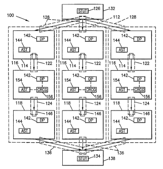
Figure 4 illustrates a telephonic switch, shown
generally at 100. Operation of an embodiment of the
present invention permits connections between various
of the circuit elements of the switch 100 to be tested
S to verify the correctness of their connections. The
switch 100 can, for example, be formed of the switch
disclosed in the aforementioned patent, U.S. Patent No.
5,347,513. Further details of the switch and its
operation are disclosed therein.
Analogous to the circuit 10, also representative
of a telephonic switch shown in Figure 1, the switch
100 includes three redundant circuit portions 112.
Each of the redundant circuit portions include first,
second, and third circuit boards 114,, 116, and 118,
1S respectively. Circuitry disposed upon the first
circuit boards 114 form conventional, terminal
connection~units which are bi-directional,
multiplexer/demultiplexer devices. While shown in
block form in the figure, the terminal connection units
may actually be a series of cascaded
multiplexer/demultiplexer devices, disposed upon a
series of circuit boards and coupled together by
couplers analogous with the couplers forming the signal
paths 22 and 24 shown in Figures 1-3.
2S Circuitry disposed upon the second boards 116 form
the switch core of the switch. And, circuitry disposed
' upon the third circuit boards 118, similar to the
circuit boards 114, form conventional, terminal
connection units. The terminal connection units may
again be a series of cascaded multiplexer/demultiplexer
CA 02238030 1998-OS-19
WO 97/2043b PCT/SE96/015b1
-16-
devices disposed upon a series of circuit boards and
coupled together by couplers.
Signal paths 122 connect the circuit boards 114
and the circuit boards 116 of the respective circuit
portions 112 together. Signal paths 124 connect to the
circuit boards 116 and 118 of the respective circuit
portions together. The signal paths 122 and 124 are
formed of electrical, optical, or other couplers.
During assembly of the telephonic switch 100, a
circuit assembler connects the various circuit boards
of the circuit portions together by coupling the
couplers forming the signals paths 122 and 124 of the
various circuit boards together. When the terminal
connection units are formed of the cascaded-together
series of multiplexer/demultiplexer devices, these
devices must also be coupled together by the assembler.
A switch termination unit terminal (STUT) 126 is
coupled to the circuit boards 114 of each of the
circuit portions 112 by way of signal paths 128, formed
of electrical, optical, or other couplers. Signals
generated by a device, here a central processor 132 are
applied to the redundant circuit portions 112 by way of
the signal paths 128, and the switch termination unit
terminal forms a portion of the central processor 132.
Only a single switch termination unit terminal 126 is
illustrated in the figure in connection with the
circuit portions 112. Additional switch termination
unit terminals 126 may also be, and typically are,
coupled to the terminalconnection units disposed upon
the circuit boards 114.
CA 02238030 1998-OS-19
WO 97/20436 PCT/SE96/0156I
_17_
' Another switch termination unit terminal 134 is
also illustrated in the figure. The switch termination
unit terminal 134 is coupled to the circuit boards 118
by way of signal paths 136, again formed of an
electrical, optical, or other coupler. The switch
termination unit terminal 134 forms a portion of a
device 138. Again, although additional switch
termination unit terminals 134 are not illustrated in
the figure, typically, a plurality of devices are
connected to the terminal connection units disposed
upon the circuit boards 118 by way of a plurality of
switch termination unit terminals 134.
Also, while not shown, connections between the
switch core disposed upon the circuit boards 116 are
formed when the telephonic switch is assembled such
that the circuit boards 116 are stacked upon one
another or plugged into a circuit backplane. Analogous
connections can be made between the terminal connection
units disposed upon the circuit boards 114 and between
the terminal connection units disposed upon the
terminal connection units 118.
The terminal connection units disposed upon each
of the circuit boards 114 and the terminal connection
units disposed upon the circuit boards 118 each include
- 25 at least either a device processor 142 and an
allocation set up terminal 144. An allocation setup
terminal is a hardware logic device. The terminal
connection units disposed upon such circuit boards also
include a plane compare/majority vote (PC/MV) device
146. The PC/MV devices 146 are operable in
CA 02238030 1998-OS-19
WO 97/2036 PCT/SE96/01561
_18_
conventional manner to poll values of signals received
at, or generated at, the circuit boards 114 and 118,
respectively.
The switch cores disposed upon the circuit boards
S 116 also each include a device processor and an
allocation set up terminal, indicated in the figure by
reference numerals 152 and 154, respectively. Either
the processor 152 or the terminal 154, or a combination
thereof, form a cyclic redundancy code to generator
(CRCG) 156. For purposes of illustration, the CRCGs
156 are separately indicated in the figure.
As examination of the illustration of the
telephonic switch 100 indicates, numerous signal paths,
signal paths 122, 124, 128, and 136 are required to be
formed during assembly of the switch. Additional
signal paths may be formed of signal paths coupling
cascaded portions of the termination connection units,
as noted previously.
Testing for the correctness of the connections
forming the various signal paths is necessary to ensure
that the correct connections have been formed during
assembly of the switch. Operation of an embodiment of
the present invention permits such determinations to be
made.
Figure 5 illustrates a portion of the telephonic
switch 100 in greater detail. The illustrated portion
includes circuit boards 114 and 116 of one of the
circuit portions 112, as described previously.
Circuitry forming a terminal connection unit is
disposed upon the circuit board114, and circuitry
CA 02238030 1998-OS-19
WO 97/20436 PCT/SE96/01561
-19-
forming the switch circuitry of a switch core is
disposed upon the circuit board 116. A signal path 122
is again shown to connect the circuit boards 114 and
116.
The terminal connection unit disposed upon the
circuit board 114 is again shown to include an
allocation set up terminal 144 and a PC/MV device 146.
As in this embodiment, the terminal connection unit
includes an allocation set up terminal 144, the
terminal connection unit does not further include a
device processor, shown in the alternative to an
allocation set up terminal in the circuit shown in
Figure 4. The plane comparator/majority voter 146 of
the terminal connection unit disposed upon the circuit
board 114 is again illustrated in the figure.
The allocation set up terminal 144 is coupled to
the signal path 122 by way of a register 158. The
terminal 144 is coupled to receive plane identification
bits on the line 162 and command signals on the line
164. Signals generated on the lines 162 and 164 can,
for example, be generated by the central processor 132,
shown in Figure 4.
The switch core disposed upon the circuit board
116 is here shown to include a device processor 152, a
cyclic redundancy code generator 156 and a register
166. The register 166 is coupled between the signal
path 122 and the device processor 152.
Once a circuit assembler has connected the coupler
forming the signal path 122 in a manner believed to
form the connection shown in Figure 5, a test to verify
CA 02238030 1998-OS-19
WO 97/20436 PCT/SE96/01561
-20-
~ for the correctness of the connection can be performed. ,
In normal protocol of communication between the
terminal connection unit and the switch core, data is
transmitted between the terminal connection unit and
the switch core in designated time slots wherein groups
of time slots together define a frame of data.
In one embodiment of the present invention,
application of plane ID signals on the line 162 and a
control signal generated on the line 164 causes
generation of a coded signal which is transmitted upon
the signal path 122. Either, or both, the plane ID
signal and the control signal can be generated by a
central processor, such as the central processor 132
shown in Figure 4. The coded signal is received by the
switch core disposed upon the circuit board 116 when
the signal path 122 has been properly connected to the
circuit board 116. Detection of the coded signal
transmitted upon the signal path 122 at the circuit
board 116 verifies that the coupler forming the signal
path 122 has been correctly connected.
Figure 6 illustrates the coded signal transmitted
in one embodiment of the present invention to test for
the correct connection of the coupler forming the
signal path 122 connecting the circuit boards 114 and
126 of the various circuit portions 112. The coded
signal here forms the two most significant bits of a
bit sequence forming a link ID updates status (LUS)
time slot which is transmitted during one frame of
data. The coded signal is identified by LID bits
formed of bits 7 and 6 of the time slot.
CA 02238030 1998-OS-19
WO 97/20436 PCT/SE96/01561
-21-
j
Other bits transmitted during the LUS time slot
are generated for other purposes and are here indicated
to include the UPDATE bits which are used between
terminal connection units for purposes of
S synchronization, STA bits and TFA bits, both of which
are used for alarm purposes. When the LID bits are of
the logical values "10", the coded signal is defined to
be active, and the receiving terminal, the device
processor of the switch core shown in Figure 5, detects
IO the presence of such signal values in the LUS time
slot.
Figure 7 also illustrates a portion of the
telephonic switch 100 shown in Figure 4. In this
illustration, the switch termination unit terminal 126
15 forming a portion of a central processor 132 is
connected to link ID transmitters 168 which are
connected to the switch termination unit terminal 126
by way of signal paths 128. The link ID transmitters
168 are formed of circuitry analogous to the circuitry
20 disposed upon the circuit board 114 forming the
terminal connection unit shown in Figure 5. The link
ID transmitters and switch termination unit terminal
form the "sending side" which transmits coded signals
to a "receiving side."
25 The transmitters 168 generate signals which are
supplied at terminal connection links 172. A terminal
' connection link 174 of a single receiving element, here
a terminal connection unit or a switch core is also
illustrated. A link ID receiver 176 formed of, for
30 example, circuit elements corresponding to the
CA 02238030 1998-OS-19
WO 97/20436 PCT/SE96/OI561
-22-
circuitry illustrated to form portions of the switch ,
core disposed upon the circuit board 116 in the
illustration of Figure 5 is also shown.
The link ID receiver 176 is further coupled to
receive plane ID signals on line 178 and is coupled to
a device processor 152. A plane comparator/majority
voter 146 is also indicated, in dash in the figure. A
test to verify the correctness of the connection of the
signal path formed of a coupler interconnecting the
sending side and receiving side is performed by
transmitting coded signals, as described above, from
the transmitters 168 and detecting their reception by
the receiver 176.
Figure 8 illustrates another portion of the
telephonic switch 100 shown in Figure 5. In this
illustration, a switch core 114 of one plane forms the
sending side which transmits the link ID sequence. A
link ID transmitter, here coupled to receive signals
generated by an allocation set up terminal and to
receive plane ID signals inserts an active, link ID bit
sequence into an LUS time slot for transmission upon a
signal path to a receiving side.
All three planes of the receiving side are shown.
Each plane includes a link ID receiver 192 which is
coupled by way of a terminal communication link 193 to
receive the link ID signal transmitted by the sending
side. The link ID receivers 192 are each coupled to a
switch termination unit terminal 134 by way of signal
paths 136.
CA 02238030 1998-OS-19
WO 97/20436 PCT/SE96/01561
-23-
Figure 9 also illustrates a portion of the
telephonic switch 100 shown in Figure 5. In this
illustration, a terminal connection unit 114 of one
plane forms the sending side which transmits the link
ID sequence. A link ID transmitter, here coupled to
receive signals generated by an allocation setup
terminal and to receive plane ID signals inserts an
active, link ID bit sequence into an LUS time~slot for
transmission upon a signal path to a receiving side.
All three planes of the receiving side are shown. Each
plane includes a link ID receiver 192 which is coupled
by way of a terminal communication link 193 to receive
the link ID signal transmitted by the sending side.
The link ID receivers 188 are each coupled to a switch
termination unit terminal 134 by way of signal paths
136.
Figure 10 illustrates another portion of the
telephonic switch 100 shown in Figure 5. In this
illustration, a terminal connection unit 124 of one
plane forms the sending side which transmits the link
ID sequence. A link ID transmitter, here coupled to
receive signals generated by an allocation setup
terminal and to receive plane ID signals inserts an
active, link ID bit sequence onto an LUS time slot for
transmission upon a signal path to a receiving side.
A terminal connection link 174 of a single
' receiving element, here a cascaded, terminal connection
unit forms a receiving side. A link ID receiver 176
formed of, for example, circuit elements corresponding
to the circuitry illustrated to form portions of a
CA 02238030 1998-OS-19
WO 97/20436 PCT/SE96/01561
-24-
terminal connection unit disposed upon the circuit
board 114 in the illustration of Figure 5 is again
shown.
Operation of an embodiment of the present
invention permits a determination to be made of the
correctness of connections formed between circuit
elements of circuit portions of a circuit having
' redundant circuit portions. Coded signals are
transmitted and detection of the coded signals
indicates correct connection of the coupler forming the
signal path. Because a coded signal is transmitted,
the connection of any type of coupler, such an optical
or other non-physical coupler, can be tested and
verified to be correct.
In the event that a misconnection is determined,
an appropriate corrective reassembly ofthe connection
between the circuit elements can be made. When the
circuit forms a telephonic switch, the coded signal,
can, as above-described, form a sequence of signal bits
generated during a single time slot of a frame
transmitted between elements of the telephonic switch.
In the event that a misconnection is detected,
reassembly of the affected portion of the switch can be
made.
The previous descriptions are of preferred
examples for implementing the invention, and the scope
of the invention should not necessarily be limited by
this description. The scope of the present invention
is defined by the following claims.