Note: Descriptions are shown in the official language in which they were submitted.
CA 02238305 1998-OS-21
WO 97/19498 PCT/US96/19682
1
MODULAR JACK CONNECTOR
FIELD OF THE INVENTION
The present invention relates generally to modular jack connectors designed to
be mounted on printed circuit boards and, more particularly, to modular jack
connectors including components for filtering common and differential mode
interference and for eliminating high frequency noise.
1o BACKGROUND OF THE INVENTION
Electrical devices are frequently subject to adverse operation in the presence
of radio frequency interference in the electrical lines connecting the devices
to, e.g.,
data communication lines. The electrical devices are not only susceptible to
such
interference, they also function as a source of such interference. Filters
must therefore
be interposed between connected electrical devices to screen out the
interference and
minimize its effect on the operation of the electrical devices.
This interference may cause two types of distortion of the power circuit wave
form, viz., common mode interference where identical wave forms are impressed
on
the electrical lines connecting the electrical devices, and differential mode
interference
2 0 _ which appears as a voltage difference between the connecting electrical
lines. Circuitry
exists to filter radio frequency interference, but for optimum effectiveness
and cost, it
has been found to be more efficient to treat the two types of interference
independently, i.e., to provide one group of electrical components to serve as
a
common mode filter and another group of electrical components to serve as a
2 5 differential mode filter.
Since electrical devices are often coupled by modular jack connectors, it is
desirable to construct modular jack connectors with integral filter components
to avoid
the need for additional, external filter components.
In addition, it is desirable for modular jack connectors mounted on printed
CA 02238305 1998-OS-21
WO 97/19498 PCT/US96/19682
2
circuit boards to eliminate noise and interference present in the electrical
connection
between the plug received in the jack and the printed circuit on which the
jack is
'
mounted. To this end, it has been suggested that line-to-ground capacitors be
incorporated in the connector to provide low impedance to high frequencies
between
the lines and ground.
One such connector is described in U.S. Patent No. 4,695,115 (Talend).
Talend discloses a modular jack in which bypass capacitors engage the contacts
in
order to pass noise and other high frequency signals to ground. The capacitors
are
end-mounted ceramic capacitors (tombstone capacitors) and are coupled at one
end
to contacts in the jack at a location between a terminal mating portion of the
contacts
and the portion ofthe contacts that engage a printed circuit board. The
capacitors are
connected at their other end to a conductive member which in turn is coupled
to a
grounding region on the printed circuit board so that the capacitors
operatively ground
the contacts.
It is a disadvantage of the structure of the Talend jack that the capacitance
is
limited since the size of the ceramic capacitors cannot be increased without
correspondingly increasing the size ofthe jack. Since it is desirable for the
jack to have
a low profile and to be as small as possible and within industry standards,
this prior art
jack is not entirely satisfactory. Further, the direct connection between the
capacitors
2 0 and the contacts detrimentally affects the intended signal passing through
the contacts.
OBJECTS ANB SUMMARX OF THE INVENTION
It is an object of the present invention to provide a new and improved modular
jack.
Another object of the present invention is to provide a new and improved
modular jack incorporating line filters and bypass capacitors.
Still another object of the present invention is to provide a practical and '
e~cient solution to the connection of a capacitor to electrical current paths
through
a connector in order to ground the current paths.
CA 02238305 1998-OS-21
WO 97/19498 PCT/US96/19682
3
' It is another object of the present invention to provide a modular jack with
capacitance means in which the disadvantages of the prior art modular jacks
are
y
substantially eliminated.
It is yet another object ofthe present invention to provide a modular jack
with
capacitance means, the capacitance of which is significantly greater than the
capacitance of bypass capacitors of prior art jacks, and wherein the size of
the modular
jack is small and within industry standards.
In accordance with the present invention, these and other objects are attained
by providing a modular jack comprising a housing, a first set of contacts for
engaging
the contacts of a mating plug connector, a second set of contacts for engaging
the
circuit of the printed circuit board on which the jack is mounted, circuit
means for
electrically coupling contacts of the first set to contacts of the second set,
a capacitor
formed of flexible sheet-like materials, preferably formed into a plurality of
folded
pleats, and a metallic shield at least partially surrounding the housing and
electrically
coupled to a ground region of the printed circuit board on which the jack is
mounted.
The capacitor includes two conductive sheet members and an intermediate
insulative
material. A first one of the conductive sheet members in the capacitor is
coupled at
one ofthe extreme capacitor pleats to contacts of the first set and a second
one of the
conductive sheet members in the capacitor engages the metallic shield at the
other
2 o extreme capacitor pleat to thereby ground the first set of contacts
through the pleated
capacitor to eliminate high frequency noise and interference. In a preferred
embodiment, the contact coupling circuit means includes a circuit board
component
arranged within the jack housing. To provide common and dii~erential mode
interference filtering, a plurality of toroidal coil pairs are mounted on the
circuit board
2 5 component in the contact coupling circuit means. A f rst group of the
toroidal coil
pairs functions as a common mode filter and a second group of the toroidal
coil pairs
' functions as a differential mode filter.
In accordance with another embodiment of the invention, the contacts of the
first set of contacts are coupled in pairs to each other and each contact pair
is coupled
CA 02238305 2000-06-07
-4-
to a capacitor, such as the pleated capacitor described above, through a
respective resistor. Only after passing through one of the resistors does the
electrical signal from the first set of contacts reach the capacitor. By means
of
this construction, the capacitor constitutes a centre point or centre mode or
centre tap for each pair of contacts of the first set of contacts and
establishes a
0-value common mode voltage at the output terminals of the connector. The
interposition of a resistor between the capacitor and each pair of contacts of
the
first set of contacts which engage the contacts of the modular plug provides
balanced signal pairs and a balanced circuit without adversely affecting the
signal.
It is also significant that only a single capacitor is required in a
jack connector according to the invention since each of the contact pairs is
connected to the capacitor via a respective resistor and the contact coupling
circuit means. Thus, the need for multiple capacitors is avoided.
The jack housing may be provided with any conventional
mounting arrangement for mounting the jack on a printed circuit board, such as
the arrangement described in U.S. Patent No. 5,244,412.
In an eight position jack according to the invention, i.e. , having
eight contacts in the first set, adapted to be coupled to a modular plug
having
only four signal-carrying contacts, only four contacts of the first set are
coupled
by the contact coupling circuit means to four contacts of the second set. The
four
remaining unused contacts of the first set are connected in pairs to each
other,
and each pair of unused contacts is coupled to the capacitor which functions
to
ground the unused contacts thereby filtering noise and interference. In this
embodiment, a resistor may be used to couple each connected pair of unused
contacts to the capacitor, in addition to the use of a resistor between
coupled
pairs of the used contacts of the first set and the capacitor, to provide a
balanced circuit.
CA 02238305 1998-OS-21
WO 97/19498 PCT/US96/19682
~ BRIEF DESCRIPTION OF TIIE DRAWINGS
Additional objects of the invention will be apparent from the following
description of the preferred embodiment thereof taken in conjunction with the
accompanying non-limiting drawings, in which:
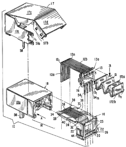
5 Fig. 1 is an exploded perspective view of a connector in accordance with the
invention;
Fig. 2 is a perspective view of the connector of Fig. 1;
Fig. 3 is a sectional view of the capacitor component of the connector taken
along line 3-3 ofFig. 1;
to Fig. 4 is a sectional view of the connector taken along line 4-4 of Fig. 2;
Fig. S is a sectional view of the connector taken along line 5-5 of Fig. 2;
Fig. 6 is a sectional view of the connector taken along line 6-6 of Fig. 4;
and
Fig. 7 is a circuit diagram of a jack connector in accordance with the
invention.
DETAILED DESCRIPTION OF TFIE PREFERRED EMBODIMENT
Referring now to Figs. 1-7 of the drawings wherein like reference characters
designate identical or corresponding parts throughout the several views, an
embodiment of a device in accordance with the present invention in the form of
a
modular jack connector 10, adapted to couple an electronic device to the
circuit of a
2 o printed circuit board through a modular plug connector, comprises a two-
part housing
14 formed of an insulative material, such as plastic, a first set of
conductive contacts
comprising a plurality of contacts 12,,...,I2ro a second set of contacts
54,,...,54"" a
circuit board assembly 13a comprising circuit means for electrically coupling
the
contacts 12 of the first set to the contacts 54 of the second set, a capacitor
15 formed
2 5 of flexible sheet-like materials formed into a plurality of folded pleats
15,,..., i SX and
a metallic shield 17 which at least partially surrounds the housing 14. The
housing 14
~ includes a first inner housing part 16 and a second outer housing part 18
which
together define a receptacle 19 adapted to receive a modular plug. A leg
portion 12a
of each of the first contacts 12,,...,12" engages a respective contact of the
modular plug
CA 02238305 1998-OS-21
..
-6-
received within the receptacle 19.
Referring to Figs. 1, 4, 5 and 6, the inner housing part 16 is
formed of an insulative plastic material and has a substantially L-
shaped configuration including a framework section comprising a
transverse base portion 20 and a pair of side portions 22 projecting
upward from both sides of the base portion 20 (Fig. 1), and a guide
section 24 extending forwardly from the top of the framework section
in a cantilever fashion. The rear side of the framework section of the
inner housing part 16 is partially closed by a pair of transverse upper
and lower walls 25 extending between the side portions 22. A
significant open space is defined at the rear side of the framework
section of the inner housing part 16 between upper and lower walls 25.
A plurality of substantially parallel guide slots or
channels 28 are formed in the top surface 30 of the guide section 24 of
the inner housing part 16 and each channel 28 is receivable of a leg
portion 12b of one of the contacts 121,...,12n (Fig. 1). Each channel 28
opens at its rearward end 32 at the open top of the framework section
of inner housing part 16 and terminates at its forward end 34 which is
recessed rearwardly of the forward edge 36 of the guide section 24 to
form fingers 38.
As best seen in Figs. 1 and 4, each of the first set of
contacts 121,...,12n has a first leg portion 12a extending though the
receptacle 19 (Fig. 4) formed in the interior of the housing 14 for
engaging a respective one of the plug contacts. The second leg portion
12b of each of the contacts 121,...,12n is positioned in a respective one of
the channels 28. The rear end of the second leg 12b of each contact 12 is
attached, e.g., by soldering, to a circuit board component 13 of the
circuit board assembly 13a. The upper end of each contact 541,...,54m of
the second set of contacts is connected to the circuit board component
13 and each second contact 54 extends through a respective bore 26
formed in the base portion 20 for connection at its lower end to the
.,
CA 02238305 1998-OS-21
_7_
printed circuit board 4 (Fig. 4).
The contact coupling circuit means that couple the
contacts 12 of the first set to the contacts 54 of the second set are
situated within the framework section of the inner housing part 16.
The contact coupling means includes the circuit board component 13
having a printed circuit including a contact element 76 (Fig. 1) and
four toroidal coil pairs 70a, 70b, 72a, 72b (Fig. 5) mounted on one side of
the circuit board component 13. Each of the toroidal coil pairs 70a, 70b
comprises a toroidal core 74b and two coils 71, 73 wound around the
core 74b. Each of the toroidal coil pairs 72a, 72b comprises a toroidal
core 74a and two coils 77, 79 wound around the core 74a.
Referring to Figs. 5 and 7, one end of coil 71 of toroidal
coil pair 70a is connected to the contact 12~ and the other end of coil 71
is connected to the contact 122. Thus, contacts 121, 122 are coupled to
each other via coil 71. Similarly, contacts 12~, 128 are coupled to each
other via coil 71 of the toroidal coil pair 70b. The other coil 73 of each
of the toroidal coil pairs 70a, 70b is connected at one end to a coil 79 of a
respective one of the toroidal coil pairs 72a, 72b and at its other end to
the coil 77 of the respective one of the toroidal coil pairs 72a, 72b. Coils
77, 79 are connected at their other ends to respective ones of the
contacts 54 of the second set of contacts, i.e., coil 79 of toroidal coil pair
72a is connected to contact 541, coil 77 of toroidal coil pair 72A is
connected to contact 542, coil 79 of toroidal coil pair 72b is connected to
contact 543, coil 77 of toroidal coil pair 72b is connected to contact 544.
Thus, as best seen in the circuit diagram shown in Fig. 7, contacts 54
are coupled in pairs to each other via coils 77 of the toroidal coil pairs
72a, 72b which are connected to coils 73 of the toroidal coil pairs 70a,
70b which in turn are connected to coils 79 of the toroidal coil pairs
72a, 72b.
Coils 71, 73 are wound around respective toroidal cores
74b in a specific manner and incorporated into the contact coupling
CA 02238305 2000-06-07
_8_
circuit means so that their current-induced inductive fluxes are additive. As
such, toroidal coil pairs 70a, 70b function as differential mode filters.
Coils 77,
79 of the toroidal coil pairs 72a, 72b are wound around toroidal core 74a
inductively opposite to each other and are equal in number of turns so that
their
current-induced fluxes substantially cancel each other. In this case, toroidal
coil
pairs 72a, 72b thus function as common mode filters. Toroidal coil pairs 72a,
72b are smaller in size than toroidal coil pairs 70a, 70b since while the
toroidal
coil pairs 72a, 72b must comply with ETHERNET specifications and have a
minimum inductance value, there is no standard industry specification for
toroidal coil pairs 72a, 72b which function as common mode filters.
With respect to the arrangement of coils on toroidal cores to form
toroidal coil pairs which function as either common mode filters or
differential
mode filters, reference is made to U.S. patent Nos. 3,996,537 and 4,263,549.
As seen most clearly in Figs. 1 and 3, the capacitor 15 is a
continuous, flexible, elongate laminate assembly formed of a laminate of a
sheet
170 of insulative material such as CAPTONTM and a pair of flexible conductive
sheet members 172a, 172b formed of wire mesh attached to respective sides of
the sheet 170 by conductive adhesive means, such as conductive paste 171 (Fig.
3). An insulative coating 173, such as non-conductive paste, is applied to the
outer surface of both the sheet members 172a, 172b with regions of the first
and
last pleats left exposed. In the illustrated embodiment, the capacitor
laminate
assembly was folded to form seven substantially equal sections or folded
pleats
151,...,15X where x=7. An exposed region of the conductive sheet member 172a
of the first pleat 151 is adjacent to and attached to the contact element 76
arranged on the circuit board component 13 and an exposed region of the
conductive sheet member
CA 02238305 1998-OS-21
- 8a -
172b of the last pleat 15~ is attached to an inner surface of the metallic
shield 17 (Fig. 4).
Although the capacitor laminate assembly in the
illustrated embodiment has six folds defining seven pleats, the
5 number of pleats in the capacitor 15 depends on the capacitance to be
obtained and the dimensions of the conductive sheet members 172a,
172b and the sheet 170 of insulative material. Thus, the capacitor 15
may even be an unfolded flexible laminate assembly provided the
capacitance provided thereby is sufficient to enable effective operation
10 of the connector.
The capacitor 15 must have an odd number of pleats, e.g.,
seven as shown, in order to maintain the proper polarity to ground,
i.e., the sheet member 172a must be electrically coupled to the circuit
means coupled to contacts 12 and the sheet member 172b must be
15 electrically coupled to the metallic shield 17.
CA 02238305 1998-OS-21
WO 97/19498 PCTlUS96/19682
9
' The construction of the capacitor i 5 in this manner, that is as a flexible
laminate
assembly formed in a plurality of folded pleats, provides significant
advantages in the
construction and operation of the connector 10. In particular, it enables a
significant
increase in the capacitance which can be provided in the small space occupied
by the
capacitor and existing in the interior of the connector. In an experimental
embodiment,
over 100 Pf of capacitance was obtained by making a five-pleated capacitor
from 0.340
x 2.0 inches of copper sheet mesh with 0.4 x 2.0 inches of CAPTON~ film. The
thickness of the capacitor was about 0.124 inches, the sheet members 172a,172b
having a thickness of about .0016 inches, the CAPTON'~ sheet 170 having a
thickness
of about .005 inches, the layer of conductive paste I7I between the sheet
members
172a,172b and the CAPTON~ sheet 170 having a thickness of about .0014 inches
and
the layer of non-conductive paste 173 on the outer surface of at least one of
the sheet
members 172a,172b having a thickness of about .0014 inches.
Referring now to Fig. 6, the circuit board component assembly 13a also
includes four resistors 78 mounted on an opposite side of the circuit board
component
13 from the side on which the toroidal coil pairs 70a,70b,72a,72b are mounted.
The
contact element 76, to which the capacitor 15 is connected via conductive
adhesion
means, is also arranged on the same side of the circuit board component 13 as
the
resistors 78 and is coupled to resistors 78 by the circuitry of circuit board
13. The
2 o circuit ofthe circuit board component 13 provides an electrical connection
from each
of the resistors 78 to the capacitor contact element 76 to which the capacitor
15 is
mounted.
In oneembodimentof the invention,a resistor 78is provided for each~air of
contacts 12 of the first set. Each resistor is coupled between each pair of
contacts 12
2 5 and the capacitor 15 to provide balanced signal pairs and a balanced
circuit without
adversely affecting the signal.
Fig. 7 illustrates a circuit diagram of the components of an eight position
jack,
i.e., a jack having eight contacts 12,...,128, in accordance with the
invention which is
adapted to be coupled to a printed circuit board 4 having only four signal-
carrying
CA 02238305 1998-OS-21
WO 97/19498 PCT/US9b/19b82
contacts. Therefore, only four contacts I2,, I2z, I2~,128 of the first set are
coupled by
the contact coupling circuit means 1:o four contacts of the second set
541,...,544. The
four unused contacts 123,...,126 of the first set are connected in pairs, 123
and 124, 125
and 126, via the appropriate electrical connections on the circuit board
component 13
5 and then each pair is connected to a resistor 78. On the other hand,
electrical
connections, which may be wires 75, are provided (shown in dotted lines in
Figs. 5 and
6) to couple the resistors 78 which are coupled to the contacts
121,12z,12~,128 to a
respective one of the coils 7 i .
The contacts 123,124 are thus connected to each other and to a single resistor
10 78 and similarly, the contacts 125,126 are connected to each other and to
another
resistor 78. Contacts 123,124,125,126 are unused and filtered. Coil 71 of the
first
toroidal coil pair 70a connects contacts I2, and 122 and another coil 71 of
the second
toroidal coil pair 70b connects contacts 12,128. Wires 75 connect each of the
coils
71 to one of the resistors 78. The circuitry on circuit board component 13
includes
connections between each of the resistors 78 and capacitor 1 S. All of the
contacts
121,...,128 are thus electrically coupled to the capacitor 15 via the
resistors 78. In view
of this arrangement, the current path from each pair of the contacts 12 is
directed to
the capacitor 15 only through one of the resistors 78 providing for balanced
signal
pairs.
2 o Referring again to Fig. I, the assembly of the jack 10 will now be
described.
The contacts 12,,...,12n are initially pre-formed with the first and second
leg portions
12a,12b as shown in Fig. 1. The circuit board component assembly 13a is also
pre-
assembled with its electrical-circuit-containing circuit board component 13,
and the
toroidal coil pairs 70a,70b,72a,72b, wires 75, capacitor contact element 76
and
resistors 78 mounted on the circuit board component 13 and the pad-engaging
contacts
54,,...,54m and contacts 12, ,...,12" connected thereto. Upon insertion of the
circuit
board assembly 13a into the framework of the inner housing part 16, the pad-
engaging
contacts 54 are inserted through aligned bores 26 in the base portion 20 of
the inner
housing part 16 and the legs 12b of contacts 12,,...,12" are inserted into
respective
CA 02238305 2000-06-07
- 11 -
ones of the channels 28 in the guide portion 24 of the inner housing part 16
such
that the first leg portions 12a thereof extend beyond the forward edge of the
channels 28.
The sub-assembly of the inner housing part 16, circuit board
assembly 13a and contacts 121, ..,12n is then inserted into the rearward space
within outer housing part 18 in the direction of arrow A as shown in Fig. 1.
During insertion, the mating contact portions, i.e., the first leg portions
12a of
contacts 121, ,..12n are aligned with respective guide slots formed in the
outer
housing part 18 between portions and engage a surface whereby the first leg
postions 12a are bent into the shape shown in Fig. 4 as insertion of the
firmer
housing part 16 into the outer housing part 18 continues. Other details of the
assembly of the inner housing part 16 into the outer housing part 18 can be
found in U.S. Patent No. 5,244,412.
Mesh sheet 172a at the first pleat 151 of the pleated capacitor 15
is electrically connected to the contact element 76 of the circuit board
component
13 by means of a conductive adhesive.
The metallic shield 17 is then applied over the outer housing part
18 of the housing 14 to surround at least a portion of the housing 14 once the
capacitor 15, circuit board assembly 13a and contacts 121, ...12n are secured
in
the housing 14. To this end, the metallic shield 17 is constructed with folds
corresponding to the edges of the outer housing part 18. To apply the metallic
shield 17 about housing 14, first side portions 17a (only one of which is
shown
in Fig. 1) and a front portion 17b (Fig. 2) of the metallic shield 17 are
positioned
abutting corresponding surfaces of the outer housing part 18, i.e. the
metallic
shield 17 is placed over the outer housing part 18 so that side portions 17a
engage side portions 18a of the housing and the front portion 17b of the
metallic
shield 17 engages with the front, substantially open side of the outer housing
part 18 (see Fig. 2).Then, the top surface 17c of the metallic shield 17 is
brought
into engagement with the top surface of the outer housing part 18. Conductive
adhesive is applied to connect the parts of the metallic shield 17 to the
outer
surface of the housing 14.
Mesh sheet 172b at the last pleat 15~ of the pleated capacitor 15
is electrically
CA 02238305 1998-OS-21
,.
s
- 12-
connected to the rear surface 17d of the metallic shield by means of a
conductive adhesive.
The rear surface 17d of the metallic shield 17 is bent about
the fold between the rear surface 17d and the top surface 17c to close a
rear side of the outer housing part 18, i.e., that side of the outer
housing part 18 which is open, through which the inner housing part
16 is inserted into the outer housing part 18 and at which the capacitor
is positioned. The rear surface 17d of the metallic shield 17 is
attached to the side portions 17a of the shield 17 by cooperating
10 fastening members 57a, 57b to securely close the shield 17 about the
housing 14. In this manner, only a lower portion of the housing 14
and the receptacle 19 for entry of the modular plug are exposed (as
shown in Fig. 2) and are not covered by the metallic shield 17. The jack
connector 10 is then attached to the printed circuit board 4 by inserting
15 the mounting posts 56 into holes 9 in the printed circuit board 4.
Electrical connection of the metallic shield 17 to the
printed cixcuit board 4 is facilitated by metallic tabs 58 extending from
the lower surface of the side portions 17a of the metallic shield 17. Tabs
58 are soldered to a grounding region 150 (Fig. 2) on the printed circuit
board 4 to operatively ground the metallic shield 17 and thus ground
the first set of contacts 121,...,12n coupled thereto through the capacitor
15 and the circuit board component 13.
The examples provided above are not meant to be
exclusive. Many other variations of the present invention would be
obvious to those skilled in the art, and are contemplated to be within
the scope of the appended claims. For example, although in the
illustrated embodiment a printed circuit board component is
contained within the connector, in a more basic embodiment, it is
possible to dispense with the printed circuit board component and
toroidal coil pairs attached thereto, and to connect the pleated capacitor
via resistors to the contacts themselves or to some electrical coupling
means which couple the contacts which engage the contacts of the
CA 02238305 1998-OS-21
- 12a -
mating plug and the contacts which engage the printed circuit board.
Also, it is possible to dispense with the circuit board component
altogether and to mount the toroidal coil pairs, resistors,
CA 02238305 1998-OS-21
WO 97/19498 PCT/US96/I9682
13
capacitor and contact coupling circuit means on the housing, e.g., interior
walls of the
housing.