Note: Descriptions are shown in the official language in which they were submitted.
CA 02238319 1998-0~-21
W O 97/20962 PCTAUS96/19408
~u~ ~ING OF Ll'l'nlU~
FIELD OF T~E INrVENTION
The present invention relates to processes for
S sputtering lithium and sputtering targets useful in such
processes.
BACKGRO ~ D OF THE INrV~NTION
In certain industrial processes, it is
necessary to add lithium to a substrate. In particular,
electrochromic devices, which are adapted to change
optical properties in response to changes in an applied
electrical potential typically include a plurality of
layers incorporating mobile lithium ions. Under the
influence of an applied potential, the lithium ions will
migrate from one layer to another. The various layers
are selected so that the optical properties change
depending upon the concentration of lithium in each
layer. Materials of this nature are disclosed, for
example, in United States Patent No. 5,370,775. These
materials can be used in optoelectronic devices such as
light modulators, display devices and the li~e.
Electrochromic materials can also be used in selectively
controllable window systems for various applications,
including windows on buildings and vehicles. Certain
2s production processes for making electrochromic materials
require application of lithium to the electrochromic
material after the same is formed. As disclosed in the
'755 patent, this can be accomplished by exposing the
electrochromic materials to an electrolytic process
using an electrolyte bearing lithium ions. Although
this process is effective, it requires exposure of the
substrate bearing the electrochromic layer to a liquid
electrolyte. This, in turn, can add to the cost of
handling substrates, particularly large substrates such
as window glass panes.
It has been proposed heretofore to use
sputtering to apply lithium to a substrate such as an
electrochromic substrate. In the sputtering, ions are
CA 02238319 1998-0~-21
WO 97/20962 PCT~US96/19408
_z_
impelled against an exposed surface of a source or
"target" formed from the material to be applied, as by
imposing an electrical potential between the target and
a counterelectrode while maintaining the target in
proximity to the substrate. The energetic ions
impacting on the target dislodge atoms of the target,
commonly referred to as "adatoms", which then deposit on
the substrate. Typically, such a process is conducted
in a gaseous atmosphere maintained under a very low
subatmospheric pressure. The gaseous atmosphere is
ionized to form a plasma, a mixture of ionized gas atoms
and free electrons. Ions of the gas form the energetic
ions which bombard the target. The potential applied
between the target and the counterelectrode ordinarily
is a fixed (DC) potential, wherein the target is
negative with respect to the counterelectrode, where the
target is a conductive material. An alternating
potential at radio frequencies (RF) typically is used
when the target is a dielectric material. Most
commonly, the radio frequencies used for such sputtering
are at the particular radio frequencies reserved by
communications authorities for industrial, scientific
and medical uses, the so-called "ISM" frequencies, most
typically about 13.56 MHZ or higher.
Targets formed from lithium compounds such as
~i2CO3 can be successfully sputtered to deposit lithium
into electrochromic materials. ln large scale syste~s,
however, the RF sputtering potential required with a
Li2CO3 target presents process problems such as
nonuniformity and requires expensive equipment for
generating and handling high power RF. It would be
desirable to use a sputtering target having an exposed
surface consisting essentially of pure, metallic
lithium. Such a metallic lithium sputtering target at
least in theor~ should provide faster more uniform
deposition of lithium into the substrate particularly in
a relatively large-scale process. As set forth in
United States Patent 5,288,381, proposals for use of a
CA 02238319 1998-0~-21
W O 97/20962 PCT~US96/19408
--3--
lithium metal target surface have been advanced.
However, there has been no practical process heretofore
for sputtering lithium from a target having a metallic
~ lithium surface. In particular, it has been impractical
to sputter lithium at a reasonably fast rate from a
target having metallic lithium at its exposed surface
using DC sputtering potential without damaging the
target. It has also been difficult to fabricate lithium
sputtering targets heretofore.
10There have, accordingly, been substantial
unmet needs for further improvements in lithium
sputtering processes. There have been further needs for
improvements in sputtering targets for use in such
processes and in methods of making such targets.
SUMMARY OF THE INVENTION
The present invention addresses these needs.
One aspect of the present invention provides
methods of sputtering lithium. Methods according to
this aspect of the invention preferably include the
steps of maintaining a target having metallic lithium on
an exposed surface in a substantially inert gas at
subatmospheric pressure together with a counterelectrode
and a substrate. The methods further include the step
of imposing a periodically reversing electrical
potential between the target and the counterelectrode so
as to form a plasma adiacent to the target and bombard
the exposed surface of the target with ions of the gas
to thereby expel lithium from the target to the
substrate. The electrical potential desirably has a
reversing frequency between about 8 kHz and about 120
kHz. Most preferably, the target includes a layer of
metallic lithium disposed on a supporting layer formed
from a metallic material such as copper or a copper-
based alloy, the lithium being metallurgically bonded to
the supporting layer.
Surprisingly, it has been found that processes
employing these conditions can allow sputtering of
lithium from a lithium surface target to proceed at a
CA 02238319 1998-0~-21
W O 97/20962 PCTAUS96/19408
-4-
substantial rate. By contrast, attempts to sputter
lithium ~rom a target with a metallic lithium surface
using a non-reversing DC potential can result in rapid
destruction of the target when high power levels are
applied. Although the present invention is not limited
to any theory o~ the cause of these difficulties, it is
believed that destruction of the target with DC
potential results from formation of a dielectric,
sputter resistant layer on the target surface, or from
lo impurities or defects in the target surface. It is
believed that these layers, impurities or ~efects build
up a static charge as DC sputtering continues, and that
arcing occurs when the static charge builds to the point
of dielectric breakdown of the insulating layer. It is
believed that the reversing potential causes dissipation
of such charges and therefore prevents arcing. Such
dielectric layers theoretically should not form in an
inert gaseous atmosphere. However, it is believed that
even when substantially pure inert gases are used as the
2~ feed stock for forming the atmosphere, and even with
scrupulous attention to purging of the reaction ch~h~,
some residual reactive gases such as oxygen and nitrogen
persist. Any reactive gases present in the system will
react with the lithium to form the insulating films
2~ during the process. Further, it is believed that
formation of the dielectric layer can begin during
exposure to air incident to handling and installation of
the target and startup of the sputtering system.
Also, it is believed that a lithium layer
metallurgically bonded to the supporting layer provides
a path for heat transfer from the ~ithium l~yer to the
supporting layer having substantially lower thermal
resistance than that which can be achieved by abutting
contact between the lithium and the supporting layer.
Moreover, it is believed that this low thermal
resistance will be maintained during the process. As
used in this disclosure, the term "metallurgical bond"
means an interface between metallic layers at which the
CA 022383l9 l998-0~-2l
W O 97/209~2 PCTAJS96/19408
--5--
metallic layers are substantially bonded to one another
and in which the interface consists essentially of
metals and intermetallic compounds. It is believed that
the metallurgically-bonded interface will not be
S susceptible to cont~ ;n~tion by oxidation or other
reactions with atmospheric cont~;n~nts during the
sputtering process. The methods preferably further
include the step of cooling the supporting layer, as by
cooling a holder which is in contact with the supporting
layer, so that heat is continually conducted from the
lithium layer into the supporting layer.
Regardless of the ~ch~nisms of operation, it
has been found that methods according to the foregoing
aspects of the present invention can be used with
surprisingly good results to sputter lithium at
substantial rates.
According to a further aspect of the present
invention, it has been found that if the target is
exposed to a '~clearing" potential including a reverse-
direction potential (target positive with respect tocounterelectrode) during one or more intervals in the
sputtering process, sputtering potentials which
otherwise would not be expected to work well, such as a
pure forward DC sputtering potential or a low frequency
AC sputtering potential, can be employed during the
rem~in~er of the sputtering process. The clearing
potential may include one or more periodic or aperiodic
pulses of reverse-direction potential interspersed with
forward-direction potential pulses, or may include a
conventional, periodic alternating potential. Most
preferably, the intervals during which the clearing
potential is applied include a first interval before
application of the sputtering potential itself. The
target should maintained in the inert atmosphere during
3S the process, from the first interval to after
termination of the sputtering potential. The process
typically is conducted in an enclosed sputtering ch~mh~r
and the chamber remains closed during the entire
CA 02238319 1998-0~-21
W O 97120962 PCTAUS96/19408
process. Any chamber opening or other exposure of the
target to the ambient atmosphere desirably is followed
by application of the clearing potential. Although the
present invention is not limited by any theory of
S operation, it is believed that application of the
reversing potential at startup removes contaminants,
such as lithium oxide leaving a very pure target surface
which in turn facilitates sputtering under the
sputtering potential.
Stated another way, the preferred processes
according to this aspect of the present invention
include the step of applying the clearing potential
before applying the sputtering potential, and then
applying the sputtering potential while maintaining the
target in the inert atmosphere. The exposed surface of
the target is thus cleaned by sputtering during
application of the cleAn; ng potential, and this cleaning
may continue during the initial application of the
sputtering potential. The ability to start with a
lithium metal target having a con~A~;nAted surface on
the target offers considerable advantages in process
design. Thus, it would require considerable care to
install a lithium target in a sputtering chamber without
somehow contA~;n~ting its surface, by even momentary
exposure to ambient air. In accordance with this aspect
of the invention, reasonable amounts of such
contA ;n~tion can be ac~ odated without disrupting the
sputtering process.
Application of the clearing potential during
further intervals, interspersed with periods of the
sputtering potential, further facilitates the process.
Although the present invention here again is not limited
by any theory of operation, it is believed that the
clearing potential counteracts the tendency of the
3S lithium metal target to form a dielectric layer on its
exposed surface during the sputtering process. Thus, the
dielectric layer is believed to form even in the
presence of a substantially inert atmosphere as used in
CA 02238319 1998-0~-21
W O 9712~g62 PCTAJS96/19408
_7_
an industrial process, due to the inevitable presence of
small amounts of contaminant gases such as oxygen and/or
nitrogen, and due to the high reactivity of lithium.
During the sputtering process, and particularly in a DC
sputtering process, the dielectric layer in turn is
~ believed to accumulate a positive charged on the side
facing the plasma, which in turn can lead to arcing with
the negatively-charged target if the dielectric layer
brea~s down. It is believed that the clearing potential
acts to dissipate the positive charge. This itself
suppresses arcing and also facilitates removal of the
dielectric layer which further suppresses arcing.
In a particularly preferred process according
to this aspect of the invention, the target is exposed
lS to an alternating potential, such as the reversing
potential ~ ed above, during inception of the
sputtering process, and DC potentials can be employed
during the L I '; nder of the sputtering process. The
target is maintained in the inert atmosphere from before
termination of the alternating potential to after
termination of the DC potential. Stated another way, if
the sputtering process is started using the alternating
potential, it can continue, at reasonable speed, using a
direct potential. The process typically is conducted in
an enclosed sputtering chamber and the ~-.hi~ h~r remains
closed during the entire process. Any chamber opening
or other exposure of the target to the ambient
atmosphere desirably is followed by application of the
reversing (AC) potential. Although the present
invention is not limited by any theory of operation, it
is believed that application of the reversing potential
at startup removes contaminants, leaving a very pure
target surface which in turn allows DC sputtering under
reasonable conditions.
3~ Preferred processes according to these aspects
of the invention provide the ability to deposit lithium
uniformly over large substrates. Although DC sputtering
can be employed as discussed above, it is preferred to
CA 02238319 1998-0~-21
W O 97/20962 PCTAJS96/19408
-8-
apply the a reversing potential, including periods of
reverse polarity, throughout the entire sputtering
process. Where the substrate includes a lithium-
intercalable material as discussed below, it has been
found that the reversing potential promotes more rapid
transfer of lithium into the substrate. The reasons for
this phenomenon are not fully understood. ~ere again,
the present invention is not limited by any theory of
operation. ~owever, it is believed that application of
the alternating potential to the target and
counterelectrode may also result in application of an
alternating potential on the substrate, and that this
potential may facilitate intercalation of the lithium
into the substrate.
The reversing potential may be a symmetrical,
sinusoidal alternating potential, or else may have other
forms such as an asymmetrical, pulsed potential which
the sputtering target is negative with respect to the
counterelectrode for the majority of the cycle and
2D positive for the minority of the cycle. The potential
more preferably has a reversing frequency between about
10 kHz and about 100 kHz.
The counterelectrode may also include a second
lithium-bearing target, in which case the second target
is sputtered during one phase of the reversing
potential. The substrate may include a lithium-
intercalable material at an exposed surface, and lithium
expelled from the target desirably intercalates into
this lithium-intercalable material. The lithium-
intercalable material may be a metal chalcogenide suchas an oxide of tungsten or vanadium. The lithium-
intercalable material may be an electrochromic material.
The process is particularly useful in treatment of
relatively large substrates. Most preferably, the
substrate is moved in a preselected direction of motion
during the potential applying step so that new regions
of the substrate are continually exposed to the expelled
lithium. The substrate may be a relatively large item
CA 02238319 1998-0~-21
W O 97/20962 PCT~US96/19408
_g_
such as a sheet or pane of window glass. The substrate
may have dimensions transverse to the movement direction
of at least about 0.2M and desirably about 0.2M to about
l.SM. Even larger substrates may be employed. The target
may incorporate a plurality of target elements, each
such target element having an exposed surface portion.
These plural target elements may be retA;n~ on a single
target holder. Most desirably, each target element
includes a top layer of metallic lithium defining the
1~ exposed surface and a metallic supporting layer, the top
layer being metallurgically bonded to the supporting
layer.
Further aspects of the present invention
provide sputtering target elements. Each such
lS sputtering target element may include a metallic
supporting layer as discussed above together with a
layer of metallic lithium overlying a front surface of
the supporting layer and metallurgically bonded to such
supporting layer. The supporting layer desirably is
formed from a metal which does not tend to form alloys
with lithium rapidly at elevated temperature.
Desirably, the metal of the supporting layer is selected
from the group consisting of copper, copper-based
alloys, nickel-plated copper and stainless steel.
Indium desirably is present as a thin coating or
interfacial layer between the lithium top layer and the
metallic supporting layer, so that the lithium layer is
bonded to the supporting layer through the indium
interface. Sputtering targets according to this aspect
of the present invention can be utilized in processes as
aforesaid. It is believed that the intimate
metallurgical bond between the lithium top layer and the
supporting layer materially enhances heat transfer from
the lithium layer to the supporting layer and to the
other components o~ the apparatus. This, in turn,
prevents melting of the lithium even at substantial
sputtering power levels.
-
CA 02238319 1998-0~-21
W O 97/20962 PCTrUS96/~9408
-10-
Further aspects of the present invention
provide methods of making sputtering targets. Methods
according to this aspect of the present invention
desirably include the steps of providing a metallic
S supporting layer, applying molten lithium to a front
surface of the supporting layer and cooling the molten
lithium to thereby solidify the lithium and form a layer
of lithium metallurgically bonded to the supporting
layer. Most preferably, the supporting layer includes,
at its front surface, a metal selected from the group
consisting of copper and copper based alloys. The step
of applying molten lithium may include the step of
juxtaposing a solid metallic lithium preferably in the
form of a sheet of metallic lithium, with the supporting
layer so that the solid lithium overlies the top surface
and melting the solid lithium.
Most preferably, the molten lithium is brought
to an elevated temperature above its melting point,
desirably at least about 230QC, and more preferably
about 240 to about 280QC, and maintained at such
elevated temperature for at least about 20 minutes while
in contact with the supporting layer. Still higher
temperatures, and longer holding times, can also be
used. Such elevated temperature and prolonged wetting
~5 time greatly facilitates wetting of the supporting layer
by the lithium and formation of a good metallurgical
bond between the lithium and the supporting layer.
Lower temperatures, typically about l90QC, can be used
if the supporting layer is thoroughly cleaned before
application of lithium. The step of providing a metallic
supporting layer may further include the step of
providing a coating of indium on the front surface of
the supporting layer. The indium layer also promotes
wetting. The step of melting the solid lithium can be
3S performed by applying heat to the supporting layer so
that heat is transferred through the supporting layer to
the solid lithium. As further discussed below, these
preferred arrangements provide for substantially uniform
CA 02238319 1998-0~-21
W O 97/20962 -11- PCT~US96/19408
application of lithium, and substantially uniform
melting of the lithium, over the extent of the front
surface. The supporting layer may have a depression in
~ its top surface and a ridge surrounding the depression.
The step of applying molten lithium may be conducted so
that the molten lithium completely fills the depression
and covers the ridge. This preferred method provides a
relatively thick portion of the lithium layer in the
depression and yet provides a thin portion of the layer
on the ridge. The thin portion can be retained at the
outer edge of the ridge by surface tension. This
provides complete coverage of the target surface support
layer. The sputtering operation desirably is conducted
so that lithium is sputtered principally from the thick
portion of the layer, as by aligning the thick portion
of the layer with the magnetic field of a magnetron-type
target holder. Thus, the target has a prolonged service
life.
These and other objects, features and
advantages of the present invention will be more readily
apparent from the detailed description of the preferred
embodiments set forth below, taken in conjunction with
the accompanying drawings.
BRIEF DESCRIPTION OF THE DRAWINGS
Fig. 1 is a diagrammatic prospective view
depicting apparatus in accordance with one embodiment of
the invention, with portions removed for clarity of
illustration.
Fig. 2 is a diagrammatic, fragmentary
sectional view taken along lines 2-2 in Fig. 1.
Fig. 3 is a diagrammatic plan view taken along
lines 3-3 in Fig. Z.
Fig. 4 is a graph of certain experimental
results.
Fig. 5 is a diagrammatic perspective view
depicting a component in accordance with a further
embodiment of the invention.
CA 02238319 1998-0~-21
W O 97/20962 PCT~US96/19408
-12-
Figs. 6 and 7 are diagrammatic perspective
views depicting portions of apparatus in accordance with
further embo~; -nts of the invention.
Fig. 8 is a graph depicting further
experimental results.
DET~Tn~n DESCRIPTION OF THE PREFERRED EMBODIMENTS
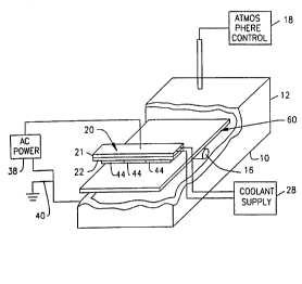
Apparatus utilized in one process of the
present invention includes an electrically grounded
metal-walled process ~hA~h~ 10 having an upstream end
12 and a downstream end 14. The process chamber is
equipped with conventional air locks or other devices
(not shown) to permit feeding of items to be treated
into the chamber through the upstream and to permit
withdrawal of the treated items at the downstream end
14. The ~h;~ hr-~- is equipped with a substrate conveyor
system schematically represented by a feed roller 16
adapted to feed flat sheet-like workpieces from the
upstream end to the downstream end. Substrate conveyor
16, and hence the substrates treated by the approaches
preferably are electrically isolated from the chamber
wall 10 and hence isolated from ground potential. The
~h~ h~n is also connected to conventional atmospheric
control apparatus 18 adapted to fill the space within
chamber 10 with an inert gas at a low subatmospheric
pressure. The atmospheric control apparatus may
incorporate conventional elements such as gas supply
cylinders, pressure regulators, vacuum pumps and the
like. The apparatus further includes a target element
holder 20. The target holder includes a generally
rectangular holder plate 21 about 40 cm long and about
13 cm wide. The rectangular holder plate is disposed
within chamber 10 and extends transversely to the
upstream to downstream direction of the chA~h~ The
target holder includes attachment devices, symbolically
3S represented by bolts 24 ext~n~i ng through the holder
plate for securing a base plate 22 to the holder plate.
Base plate 22 is provided with cooling fluid chAn~el~
26, which in turn are connected to a coolant supply unit
,
CA 02238319 1998-0~-21
W O 97/2~962 PCT~US96/19408
-13-
28 (Fig. 1). The coolant supply unit is adapted to
circulate a liquid through the coolant channels 26, and
to maintain such li~uid at a controlled temperature,
- thereby controlling the temperature of the base plate
22. Base plate 22 has a front surface 30 facing away
from the wall of the ~h~her. The target holder 20
includes conventional magnetron equipment 32 adapted to
project magnetic flux through the front face 30 of the
base plate, and to provide such magnetic flux over a
predetermined zone of the front face. This zone 34,
indicated by broken lines in Fig. 3, is generally in the
shape of an oval loop or "racetrack" and is oriented
with its long dimension transverse to the upstream to
downstream direction of the chamber. Holder plate 21 is
electrically connected to a conductor 36, which in turn
is electrically insulated from housing 10. Conductor 36
is connected to one side of an AC power source 38. The
opposite side of the power source is connected to ground
40 and to the metallic wall 10 of the chamber.
2~ A sputter target element 44 in accordance with
an embodiment of the invention includes a supporting
layer 46 having a front surface 48 and a rear surface
50. supporting layer 46 includes a metal at its front
surface 48. This metal should have good thermal
conductivity, but should not tend to diffuse rapidly
into lithium so as to contA in~te lithium remote from
the supporting layer with the supporting layer metal
when the supporting layer is held in intimate contact
with lithium under elevated temperatures. The metal
desirably is selected from the group consisting of
stainless steel, copper and copper-based alloys. As
used in this disclosure, the term "copper-based alloy"
means an alloy including more than 50% copper.
Substantially pure copper is preferred. Supporting
layer 46 desirably is entirely metallic. Preferably,
supporting layer 46 is of a uniform composition
throughout its thickness, from its from surface 48 to
its back surface 50. However, other arrangements may be
CA 02238319 1998-0~-21
W O 97/20962 PCTAUS96/19408
-14-
used. For example, the supporting layer may include
metals of other compositions at locations remote from
the front surface. Supporting layer 46 has a thin
coating 54 of indium on its front surface 48. Coating
54 is substantially continuous over the entire front
surface 48. Each target element 44 also includes a
front layer 56 of metallic lithium covering the front
surface of the supporting layer and hence covering the
indium coating 54. AB used in this disclosure, the term
"metallic lithium" refers to ~; pocitions consisting
essentially of metals wherein lithium is the predominant
metal, accounting for more than about 75% of the metals
in the composition and most preferably accounting for
about 100% of the composition. Essentially pure lithium
is the most preferred form of metallic lithium, although
alloys of lithium with other metals may be employed. The
front layer 56 is metallurgically bonded to the
supporting layer through the indium coating. The indium
coating desirably includes only the ;ni 1~ amount of
indium required to form a continuous layer on the
surface. Thus, the indium layer desirably is only a few
microns thick. This layer is essentially invisible in
the structure; it exists as a layer of relatively high
indium concentration at the interface between the
metallic lithium of the front layer and the metal of the
support layer. Preferably, the lithium front layer,
prior to use of the target element, is between about lmm
and about 10 mm thick.
Each sputter target element 44 may be
fabricated by first cleaning the supporting layer 46 and
etching it in an acid bath, preferably hydrochloric
acid. After removal of acid residue as by a distilled
water rinse, the supporting layer is transferred into an
enclosed working chamber such as a glove box maintained
under a dry, substantially inert atmosphere such as dry,
essentially oxygen-free argon. To assure cleanliness,
the atmosphere in the ~h~h~ is purified by melting a
mass of scrap lithium within the glove box before
,
CA 02238319 1998-0~-21
W O 97/20962 -15- PCTAUS96/19408
cleaning the target. The molten scrap lithium reacts
with or "gets" any contaminant gasses from the rhA h~r
atmosphere. The molten scrap lithium may be maintained
in the working ~-.h;-r~h-~r throughout the target fabrication
process. The supporting layer is placed on a heater,
such as a laboratory hotplate, with the front surface 48
facing upwardly. The front surface should be level,
i.e., as close to a true horizontal surface as possible.
The heater is operated to supply heat to the rear
surface 50 and thus transfer heat through the supporting
layer. While the supporting layer is heated, a thin
coating of indium is app}ied by depositing a small
amount of indium on the front surface. The indium tends
to flow and wet the front surface. This action may be
facilitated by ~echAnically agitating the lithium with
stainless steel brushes. The amount of indium utilized
need only be sufficient to fully wet the front surface,
and form a substantially continuous film over the entire
front surface.
After application of the indium, a layer of
molten lithium is applied. The molten lithium may be
applied by depositing clean, solid lithium on the front
surface. Individual pieces of lithium can be applied at
spaced apart locations on the front surface. More
2S preferably, however, solid lithium is applied as a sheet
of substantially uniform thickness covering
substantially the entire front surface of the supporting
layer. The temperature of the supporting layer should
be maintained as uniform as possible during the heating
step. As the temperature of the supporting layer
reaches about 180QC the solid lithium melts and forms a
layer of molten lithium on the front surface. During
this process, a substantially inert wall or dam, such as
a stainless steel sheet can be maintained around the
edges of the front surface to confine the molten
lithium. Alternatively, the surface tension of the
molten lithium can be used to retain the molten lithium
layer on the support layer. After melting of the lithium
CA 022383l9 l99X-0~-2l
W O 97t209~2 PCTnUS96/19408
-16-
and wetting of the indium-coated surface by the molten
lithium, the assembly is allowed to cool under the dry,
inert atmosphere. After cooling, the fi~i~h~ target
preserved in an inert atmosphere, as by packaging it in
S a sealed container under dry inert gas.
In an alternative process, the indium coating
is omitted, and the heating of the cupporting layer and
the molten lithium is continued after the lithium layer
has fully melted, so that the molten lithium reaches a
temperature substantially above its melting (liquidus)
temperature while in contact with the supporting layer.
Preferably, the molten lithium, and the supporting layer
in contact therewith, are heated to an elevated
t~mrerature of at least about 230QC and more preferably
lS about 240QC to about 280QC, and maintained at this
temperature for at least about 10 minutes and more
preferably at least about 20 minutes. Such elevated
temperature treatment promotes wetting and formation of
a metallurgical bond between the lithium and the
supporting layer. The indium layer can be used in with
the elevated t~mr~ature treatment as well.
The sputtering target is secured to the base
plate 22 by a layer of a thermally conductive adhesive,
such as a silver filled epoxy layer 58 between the rear
surface 50 of the target supporting layer and the front
surface 30 of the base plate. The thermally conducting
epoxy may be a silver filled epoxy. Preferably, the
epoxy is capable of withst~n~ing temperatures up to
about 180QC and desirably can withstand even higher
temperatures. Layer 58 should be as thin as possible,
but should be substantially continuous over the mating
surfaces of the parts to provide the best possible heat
transfer.
As best seen in Fig. 3, a plurality of
3S generally rectangular target elements 44 are secured to
base plate 22 in end-to-end arrangement, so that the
target elements together cover the magnetic field zone
34 of the target holder 20. Thus, the plural target
CA 022383l9 l998-0~-2l
W O 97/20962 PCT/JS96/19~08
-17-
elements form an array of target elements extl~r~l inq
transverse to the upstream-to-downstream direction of
chamber 10.
In a sputtering process according to one
embodiment of the invention, target elements as
- discussed above are secured on target holder 20. A
substrate 60 such as a plate or sheet of glass with a
layer 62 of a lithium intercalable electrochromic
material is advanced through the c-h;~ h~ in the upstream
to downstream direction by conveying device 16. As
used in this disclosure, the term "electrochromic
material" refers to a material or combination of
materials which can be used alone or in combination with
other materials to provide an electrochromic effect.
Layer 62 faces towards the metallic lithium from layers
of the target elements 44. The substrate desirably
moves at a rate of about 10-20 cm/min, although any rate
of movement can be employed depending on the amount of
lithium to be deposited on the substrate. The surface of
the substrate to be treated may be at any convenient
distance from the exposed surfaces of the target
elements as, for example, about 7-8 cm. Every portion of
the substrate passes in front of a target element 44.
Atmospheric control unit 18 is actuated to maintain an
atmosphere of substantially pure, dry argon at a
pressure between about 1 and about 100 milliTorr, and
most preferably at about 10 milliTorr.
AC power unit 38 is actuated to impose an
alternating potential on leads 36, and hence on holder
plates 21, base plates 22 and target elements 44. The
alternating potential has a frequency of about 120 kHz,
more preferably about 10 kHz to about 100 kHz and most
- preferably about 10 kHz to about 40 kHz. The power
source is regulated to apply a substantially constant
power level. Preferably, the power level is regulated
to between about 0.2 and about 7 watts per cm? and
preferably about 0.2 to about 3.5 watts per cm2 of
target element front surface. Another measure of power
CA 02238319 1998-0~-21
W O 97/20962 PCT~US96/19408
-18-
density in the process is power per unit length of the
loop or racetrack region 34. Using this measure, the
- applied power should be between about 0.15 and about 4
watts per millimeter of loop length and preferably about
S between 0.15 and about 2.5 watts per millimeter. The
applied power converts the argon gas in the vicinity of
the target elements to a plasma. ~he magnetic field
provided by magnetic elements 32 enhances formation of
the plasma in the vicinity of the target elemen~s.
Thus, the gas in the chamber remote from the target
elements remains largely unionized.
During each cycle of the applied potential,
the electrode assemblies, including base plates 22, go
to a negative electrical potential with respect to
ground. During this phase of the cycle, positively
charged argon ions from the plasma are accelerated
towards the target element and impact upon the surface
of the lithium layer, thus dislodging lithium atoms.
The dislodged lithium atoms pass to the substrate and
intercalate into the lithium intercalable layer 62.
If the target elements have been exposed to
ambient air or other reactive gases during installation
and start up, the voltage developed across AC power
source 38 at the start of the process will be relatively
high. It is believed that this high voltage is caused
by contAm;n~nts, such as oxides, nitrides or hydrides
formed by reaction of the lithium with the ambient
atmosphere. These cont~ in~nts can be removed by
continued sputtering under the argon atmosphere. Even
with a substantial amount of contA in~tion, which may
result from a full day's exposure of the target surfaces
to ambient air, the sputtering operation can be
conducted without appreciable arcing or destruction of
the target elements. During this initial sputtering,
3S essentially no lithium is removed from the target.
However, upon continued operation in this mode, the
contA inAntS are removed and the voltage drops to its
normal, steady state value, whereupon a transfer of
CA 02238319 1998-0~-21
W O 97/20962 PCTAUS96119408
-19-
lithium from the target elements continues to the normal
rate for an uncontaminated target. The ability of the
process to withstand contA in~tion of the lithium
sputtering target surfaces is particularly important in
industrial operation, as it allows reasonable handling
and equipment maint~ procedures.
During the process, a substantial portion of
the power applied by unit 38 is dissipated as heat is
applied to the lithium layers in the target elements.
The metallurgical bond at the interface between each
lithium layer and the supporting substrate layer 46
allows good conduction of heat from the lithium layer to
a supporting layer. Heat is removed from the supporting
layer through the silver loaded epoxy layer 58 and ba~e
plate 22 to the cooling channels 26 and thus to the
coolant circulated by supply unit 28.
Numerous variations and combinations of the
features described above can be utilized without
departing from the present invention. For example, the
number of target elements, and the size of each target
element, can be varied as desired to provide sputter
coating of essentially any size substrate. Also, it is
not essential to move the substrate during the
sputtering process if all of the substrate can be
accommodated in the vicinity of the sputtering target
surface, or if the target itself is moved. Inert gases
other than argon can be employed. For example, helium
can be used. Helium has an atomic mass close to that of
lithium. Similarity of atomic mass promotes efficient
sputtering. Substrates other than electrochromic
materials can be treated. Also, essentially any
suitable m~ch~nical fastening arrangement can be used
for securing the base plate 22 to the electrode holder.
Thus, other means such as clamps, interlocking parts or
pins can be used to secure the base plate and hence the
target element to the electrode assembly of the
apparatus. Typically, the configuration of these
CA 02238319 1998-0~-21
W O 97/20962 PCT~US96/19408
-20-
elements is set by the configuration of the electrode
holder itself.
A sputtering target element 144 in accordance
with a further ~hoAi~ept of the invention (Fig. 5)
S includes a supporting layer 146. The supporting layer
has a top surface 148 with a depression 147 and a ridge
149 surro~ln~ing the depression and defining the edges of
the top surface. A top layer 156 of metallic lithium
overlies the supporting layer. The top layer covers the
entire supporting layer top surface, including
depression 147 and ridge 149. The top surface of the
top layer is substantially flat or bulged slightly
upwardly in the center. The top layer thus includes a
relatively thick portion 155 overlying depression 147
and a relatively thin portion overlying ridge 149.
A target element in accordance with this
~ hl~Ai ?rt of the invention can be made by applying
molten lithium to the top surface of the supporting
layer and agitating the lithium using stainless steel
brushes so as to spread the lithium over the entire top
surface. Wetting of bare copper, by lithium, without an
indium layer, can be promoted by such agitation and by
heating the assembly well above the melting point of
lithium. Thus, where no indium layer is used, the
assembly desirably is heated to about 240-280QC, most
preferably about 260Q C, to promote wetting. The molten
lithium is effectively confined by surface tension at
the outer edges of ridge 149. Because only a thin layer
of lithium is present at the ridge, the pressure exerted
by the molten lithium is mi~i ~1 and is effectively
counteracted by surface tension. There is normally no
need for external dams or barriers at the edges.
In use, target 144 is fastened to a base plate
122 which in turn is secured to a target holder 121.
Holder 121 includes magnetic elements 132 similar to
those discussed above, which provide a magnetic field in
a magnetic field region 134. Target 144 is secured to
holder 121 so that depression 147 and the thick portion
CA 02238319 1998-0~-21
W O 97/20962 PCT~US96/1~408
-21-
155 of the top layer are aligned with magnetic field
region 134. The intensity of the plasma, and hence the
rate of sputtering are far higher rate in the magnetic
~ field region than in other areas. Therefore, lithium
S will be sputtered principally from the thick portion of
the top layer. The thick portion allows extended use of
the target.
As shown in Fig. 6, two lithium-bearing
targets 244 and 245 can be connected to opposite sides
of an AC power supply 238. These targets are disposed
within the chamber of sputtering apparatus as described
above. During one phase of the AC power cycle, the
first target 244 is negative with respect to the second
target 245, and hence lithium i5 sputtered from the
first target. During this phase, the second target 245
serves as the counterelectrode. During the next phase,
the second target 245 is negative and serves as the
source of sputtered lithium, whereas the first target
serves as the counterelectrode.
As shown in Fig. 7, counterelectrodes 345
formed separately from the sputtering chamber can be
used. These counterelectrodes can be formed from
relatively inert, sputter-resistant materials such as
stainless steel. The counterelectrodes can be disposed
within the chamber adjacent to the lithium-bearing
target 344. Location of the counterelectrodes can be
adjusted for optimum sputtering speed and uniformity.
The counterelectrodes can be connected to one side of a
power supply 338 and connected though a high impedance
339, desirably about 500 ohms or more, to ground. The
other side of power supply 338 is connected to the
target, whereas the chamber wall is grounded.
The preferred embodiments discussed above
utilize reversing or alternating potential (AC)
throughout the entire sputtering process. In further
embodiments of the invention, the reversing potential is
applied as a clearing potential during a first interval
at the beginning of the process, followed by a
CA 02238319 1998-0~-21
W O 97/20962 PCT~US96/19408 -22-
sputtering potential in the form of a direct potential
(DC) in which the target is negative and the
counterelectrode is positive. Desirably, the target
remains within the protected environment of the closed
sputtering ~ h~- from the beginning of the first
interval or AC potential until the end of the DC or
sputtering potential. The DC potential may be c ?nced
before termination of the Ac potential, upon such
termination or after such termination. However, any
idle or no-potential time between termination of the
clearing or AC potential and c_ encement of the DC or
sputtering potential should brief, desirably less than a
day and more preferably less than an hour. I~ the
chamber is opened and the target is exposed to ambient
air for any appreciable time, the AC potential should be
repeated. In this arrangement, it is preferred to use
AC potentials in the frequency ranges discussed above.
However, if the AC potential is used only for startup,
and the potential is switched to ~C before usable
substrates are processed, then process uniformity during
the AC portion of the operation will be less critical.
In this case, the reversing potential can be a radio
frequency potential without impairing process
uniformity. This approach is less preferred because of
the other drawbacks associated with RF apparatus.
The reversing potential employed as the clearing
potential is not limited to a conventional, fixed
frequency symmetrical alternating potential such as a
conventional sinusoidal AC. Merely by way of example,
the clearing potential may include one or more pulses
of reverse-direction potential (target positive with
respect to the counterelectrode) interspersed with a
series of forward-potential pulses during each said
interval. The reverse potential applied during each
pulse of reverse-direction potential may be of the same
magnitude as the forward potential employed during
sputtering, or, preferably, of a lesser magnitude. For
example, where a forward DC potential of about 200
CA 02238319 1998-0~-21
W O 97/20962 PCTAJS96/19408 -23-
volts is used for sputtering, the reverse-direction
potential used in the clearing intervals may be about 10
to about 200 volts. Also, the reverse-direction pulse
may be the same length, longer, or, preferably, shorter,
than the forward-potential pulses interspersed
- therewith. For example, each interval of clearing
potential may include reverse-potential pulses between
about l~s and about lO~s long interspersed with
forward-potential pulses between about lO~s and about
lOO~s long.
The sputtering potential also is not limited
to a direct potential. For example, the sputtering
potential may be an alternating potential having a first
frequency, whereas the clearing potential may be an
alternating potential having a second, higher frequency.
As these and other variations and combinations
of the features described above can be utilized, the
foregoing description of the preferred embodiments
should be taken by way of illustration rather than by
way of limitation of the invention as defined by the
claims.
Certain aspects of the invention are further
illustrated by the following non-limiting examples:
EXAMPLE 1
A generally rectangular target element as
described above, with a lithium surface about 38 cm long
and 12 cm wide is fabricated by casting lithium on an
oxygen-free hard copper supporting layer about 3.2 mm
thick. The lithium layer is about 5 mm thick. The
supporting layer is secured to the backing plate of an
MRC (Materials Research Corporation ) 903 sputtering
cathode assembly using a silver-loaded epoxy. The epoxy
is cured by baking at about 60~C for three hours and
the assembly is then stored overnight at ambient
temperature. The assembly is maintained in an argon
atmosphere during epoxy curing and during storage until
use.
CA 02238319 1998-0~-21
W O 97/20962 PCT~US96/19408 -24-
Substrates are fabricated by providing glass
sheets with a thin, transparent layer of an electrically
conductive oxide and then sputtering tungsten onto the
oxide layer of the sheet in an oxidizing atmosphere to
form a layer of W03. Substrates made using a tungsten
sputtering current of 8 amperes are referred to as "8
amp W03" whereas other substrates, prepared using a
tungsten sputtering current of 9 amperes are referred to
as "9 amp Wo3". The 9 amp W03 samples have a thicker
layer of W03 on the glass. Substrates are coated by
passing them back and forth repeatedly under the lithium
sputtering target while sputtering lithium from the
target. During this operation, the long direction of
the sputtering target is maintained transverse to the
direction of motion of the substrate. The substrate
moves at a speed of about 15 cm/min. A sputtering
potential is applied at 40 kHz.
The W03 layer on the substrate b~cr -~ dar~er
as lithium intercalates into it. Accordingly, light
trans~ission through the substrate is measured and the
change in light trAn~ ion is used as a measure of the
amount of lithium sputtered onto the substrate. The
results are shown in Fig. 4. The process operates
stably at power levels up to 550 watts.
~5 For comparison purposes, the same apparatus is
used to sputter lithium carbonate (Li2C03) using radio
frequency power. These results are also indicated in
~ig. 4 by the curve indicated as "dTLI2C03 700 watt. . ."
The data shown in Fig. 4 indicate that
sputtering from a metallic lithium target with 250 watts
of sputtering power transfers enough lithium to cause a
65% change in light tr~n~i~ion through an 8 amp W03
layer in three passes of the substrate under the target
(curve 100). By contrast, using 700 watts applied RF
power with an Li2Co3 sputtering target, with a similar 8
amp W03 layer, requires approximately 13-14 passes to
reach the same level of light transmission and hence the
same level of lithiation. (curve 102)
CA 02238319 1998-0~-21
W O 97/20962 -25- PCTrUS96/19408
EX~MPLE 2
Using procedures similar to those of Example
1, a series of test runs using AC and DC potentials are
made with a single target in a single çh~ h~r, The
target remains in the r-hA he~ and the chamber is
- maintained under the inert atmosphere from the beg; n~ i ng
of the first run to the end of the last run. Here
again, the lithium transfer to the glass sheets is
measured by the percent light transmission (%T, Fig. 8)
after exposure; lower values of %T indicate more
lithiation. The graph of Fig. 8 shows the results for
the various runs in the order in which the runs were
made, with later runs to the right as seen in the
drawing. Values of %T for runs with AC potential are
shown as distance below axis 400 in Fig. 8, whereas
values for runs with DC potential are shown above the
axis. In both cases, points closer to axis 400
represent greater degrees of lithiation. The first run
402 after the ch~mh~ is closed is made using AC
potential. Subse~uent runs demonstrate that although a
reasonable degree of lithiation is achieved with the ~C
runs, the AC runs yield a higher degree of lithiation.