Note: Descriptions are shown in the official language in which they were submitted.
CA 0223849~ 1998-0~-2~
WO 98/13806 PCT/US97/16465
POWER SUPPLY INPUT CIRCUIT
FOR F I33LD INS TRUMENT
BACKGROUND OF THE INVENTION
The present invention relates to a field
instrument. More specifically, the present invention
relates to an input circuit in the field instrument
which receives power from a communication loop.
Process control systems ~are used in
manufacturing and other process control environments to
monitor and control the operation o~ processes. In a
conventional process control system, instruments are
placed in the field to implement the process control
Such instruments (which are typically referred to as
field instruments or transmitters) may typically include
a peripheral device, and circuitry to support the
peripheral device. The field instrument is coupled to
a communication loop (i.e., a network segment o~ the
process control system) and transmits information over
th~ communication loop to other portions of the process
control system. The communication loop is typically a
two-wire loop which provides power for operation of the
field instrument. Communication is accomplished over
the loop through a field bus standard which is a digital
communications protocol.
The field instruments may typically include a
transmitter, a process variable control circuit or a
field mounted controller. A transmitter includes a
~ sensor which is placed in the ~ield and monitors a
variable of the process, such as pressure, temperature
or ~low The transmitter is coupled to the
communication loop and transmits information over the
communication loop to a controller which monitors
operation of the process. Transmitter communication
CA 0223849~ 1998-0~-2~
WO98/13806 PCT~S97116465
using the field hus standard allows more than one
transmitter to be coupled to a single communication loop
to transmit the sensed process variable to the control
room. The ~ield bus standard describing this
communication is described in ISA 50.02-1992 Section ll.
The HART~ s~andard is another communication standard
which allows digital communication over a 4-20 mA
process variable signal.
If the field instrument includes a process
variable control circuit, the peripheral is typically a
valve or other controllable device ~or controlling some
aspect o~ the process. The position o~ the valve, along
with other desired parameters, are monitored and the
valve i5 controlled by the process variable control
circuit to a desired position. Conventional process
variable control circuits include a microprocessor, a
microcontroller, or other suitable controller which
performs calculations and signal correction, and which
also facilitates communication over the communication
loop.
If the ~ield instrument is a field mounted
controller, it does not include a peripheral device per
se. Instead, it is coupled to the communication loop
and may typically poll a plurality of transmitters to
~5 receive a signal indicative of a sensed parameter or
parameters. The ~ield mounted controller then per~orms
a desired calculation and provides a resultant signal
over the communication loop ~or use in other portions o~
the process control system.
In any case, the field instr~ment is powered
by the communication loop either by an AC current, or by
a DC voltage. When an AC current is applied, an input
circuit in the ~ield instrument rectifies the AC signal
so that it can be provided to the remainder o~ the
CA 0223849~ 1998-0~-2~
WO98/13806 PCT~S97/16465
--3--
circuitry in the field instrument. When a DC voltage is
applied, it is desirable that the field instrument be
configured so that the DC voltage supply can be
connected to the field instrument in either polarity
(i.e., the field instrument will operate regardless of
the particular orientation taken by the positive and
negative power supply terminals relative to the field
instrument).
Prior field instruments have included a diode
bridge rectifier circuit. However, such a circuit
introduces a voltage drop thereacross of approximately
0.6 vclts to 1.4 volts. Therefore, the voltage
available to the rest of the field instrument is
signi~icantly less than that provided by the terminals
of the power supply. This reduces both the power
efficiency and the maximum output voltage of the bridge
rectifier.
SUMMARY OF THE INVENTION
A field instrument includes an input circuit
which is configured with a transistor bridge rectifier
couplable to a power supply. The transistor bridge
recti~ier is con~igured to provide power from the power
supply to a remainder of the ~ield instrument.
In one preferred embodiment, the ~ield
instrument includes a peripheral which is a controllable
device ~or controlling a process variable. Such a
device may typically be a valve. A peripheral accessing
circuit includes a process variable control circuit for
controlling the valve.
In another embodiment, the peripheral includes
a sensor for sensing a process variable. The peripheral
accessing circuit includes a transmitter ~or receiving
a sensor signal provided by the sensor and transmitting
it to a control apparatus which receives the sensor
CA 0223849~ 1998-0~-2~
WO98113806 PCT~S97/16465
signal and controls a process based on the sensor signal
received.
In yet another embodiment, the field
instrument includes a ~ield mounted controller The
controller is coupled for communication over a
communication loop.
BRIEF DESCRIPTION OF TH~ DRAWINGS
FIG l is a simplified block diagram o~ a
field instrument in accordance with the present
invention coupled to a communication loop.
FIG. 2 shows an input circuit in accordance
with the prior art.
FIG. 3 shows one embodiment of an input
circuit according to the present invention.
FIG. 4 shows a second embodiment o~ an input
circuit according to the present invention.
FIG. 5 shows a portion of an input circuit
implementing a second embodiment of the present
invention.
FIG. 6 shows a portion of the input circuit of
FIG. 5 in greater detail.
FIG 7 shows an implementation o~ the present
invention in a field bus multidrop configuration.
DETAILED DESCRIPTION OF THE PREFERRED EMBODIMENTS
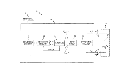
FIG. l is a simplified block diagram of a
~ield instrument lO according to the present invention.
Field instrument lO can be configured as a transmitter,
a process variable controller, or a field mounted
controller. In the embodiments in which ~ield
instrument l0 is configured as a transmitter or a
process variable controller, ~ield instrument l0
includes peripheral 12 and peripheral accessing circuit
14. Peripheral accessing circuit 14 is coupled to
communication loop 16. In the embodiment in which field
CA 0223849~ l998-0~-2~
WO98/13806 PCT~S97fl6465
-5-
instrument 10 is configured as a field mounted
controller, it may not have peripheral 12 (or converter
circuit 21 described below).
Communication loop 16 is optionally a 4-20 mA
loop which is coupled to control room or power supply
15. Control room 15 can be modeled as a voltage supply
17 in series with a resistor 19, in a known manner.
Field instrument lO is wholly powered by
communication loop 16 and can be operated either in a
current mode or in a voltage mode. In the current mode,
the power supplied to ~ield instrument lO is realized by
applying a current through communication loop 16 to the
input terminals o~ field instrument lO. In one
pre~erred embodiment, the power supply is based on an AC
current at approximately 16 kHz. A communication signal
is superimposed over the AC current at a ~requency o~
approximately l mHz.
In the voltage mode, the power supplied to
~ield instrument lO is realized by placing a symmetric
voltage via communication loop 16 across the input
terminals o~ ~ield instrument lO. In the voltage mode,
the wires coupled to the terminals o~ field instrument
10 also carry the digital communication signal. In one
preferred embodiment, each field instrument lO is
considered to be a current sink pulling approximately lO
mA o~ current from loop 16. The communication signals
are superimposed on the lO mA supply current signal with
a peak level o~ approximately 9 mA.
I~ field instrument lO is configured as a
transmitter or a process variable control circuit, ~ield
instrument lO includes peripheral 12, converter circuit
21, processing circuitry 22, interface circuit 24,
supply input circuit 26 and optional capacitance
isolation circuit 25. I~ field instrument lO is
CA 0223849~ l998-0~-2~
WOg8/~3806 PCT~S97/16465
con~igured as a transmitter, peripheral 12 is a sensor
which senses a process variable which is related to a
parameter of the process, such as temperature, pressure
or ~1OW. Peripheral 12 provides a sensor signal
indicative of the process variable to converter 21 which
converts the signal into digital form and provides it to
processing circuitr~ 22 which processes the process
variable. Processing circuitry 2Z may correct for
errors in (or compensate) the sensor or perform other
calculations on the process variable and is realized in
the form of a microprocessor. The processing circuitry
22 is coupled to interface circuitry 24 and controls
inter~ace circuitry 24 to transmit a signal indicative
of the corrected process variable over communication
loop 16 via input circuit 26 and optional capacitance
isolation circuit 25.
In the embodiment in which field instrument lO
includes a process variable control circuit, peripheral
12 typically includes a controllable device, such as a
valve or a switch, for controlling some parameter of the
process under control. Processing circuitry 22, in this
embodiment, typically includes a microprocessor, a
microcontroller, or other suitable control circuit for
receiving commands over communication loop 16, via
interface 2~, and for controlling peripheral 12 based on
the commands received. ~n this embodiment, converter
circuit 21 is a digital-to-analog converter, or other
suitable converter, which converts the digital control
signal ~rom circuit 22 to an analog signal lor maintains
it as a digital signal, as appropriate) which is applied
to the valve comprising peripheral device 12. In this
embodiment, field instrument lO can also include a
current-to-pressure controller. Processing circuitry 22
receives a control current over communication loop 16,
CA 0223849~ l998-0~-2~
WO98/13806 PCT~S97/16465
via interface 24, and converts the control current to a
pressure such as by controlling a valve. Processing
circuitry 22, in such an embodiment, would also receive
~eedback ~rom peripheral device 12 in accomplishing such
control
In the embodiment in which field instrument 10
is a field mounted controller, it may not have an
associated peripheral device 12 or converter circuit 21
Rather, the controller polls one or more transmitters
and receives signals indicative of the sensed parameters
over communication loop 16 Processing circuitry 22
performs desired calculations based on the signals
received and provides a resultant output signal over
loop 16 to be used in other portions of the process
control environment.
Capacitance isolation circuit 25 is optional
and is described in greater detail in U S Patent
Application serial number 08/225,237 filed on June 7,
1994, assigned to the same assignee as the present
application and entitled TR~NSMITTER WITH ELECTRICAL
CIRCUITRY FOR INHIBITING DISCHARGE OF STORED ENERGY,
which is incorporated herein by re~erence Briefly,
capacitance isolation circuit 25 includes an isolation
network coupled between the remainder of the circuitry
in field instrument 10 and communication loop 16 The
isolation network works to prevent discharge o~ energy
stored in the effective capacitance o~ ~ield instrument
10 onto the communication loop 16.
Supply input circuit 26 per~orms a number o~
functions If field instrument 10 is operated in the
current mode (in which the power signal supplied to
field instrument 10 is in the form of an AC current),
then supply input circuit 26 recti~ies the AC current so
that it is usable to supply power to the remainder of
CA 0223849~ 1998-05-2~
WO98113806 PCT~S97/16465
~ield instrument lO If field instrument lO is operated
in the voltage mode (in which the power signal supplied
to ~ield instrument lO is in the form of a DC voltage)
input circuit 26 is con~igured to allow the DC input
supply to be connected to field instrument lO in either
polarity. Thus, it is not important that the operator
ins~alling the system connect the supply in any
particular polarity.
FIG. 2 ls a schematic diagram of supply input
circuit 26 ' according to the prior art. Circuit 26'
includes diodes Dl, D2, D3 and D4 which are connected in
a diode bridge rectifier configuration Circuit 26~ has
disadvantages which are clearly illustrated when it is
assumed that the field instrument containing circuit 26'
is operated in the voltage mode. In that case, a DC
voltage is applied across the terminals of communication
loop 16 SO that each o~ the two terminals are at a
di~erent voltage potential (either VIN1 or VIN2) -
Depending on the polarity of the supply (i.e., depending
2~ on which terminal of communication loop 16 the operator
has connected to which terminal o~ ~ield instrument lO)
either VIN1 or VIN2 will have a higher voltage potential.
The present discussion will proceed under the assumption
that VIN1 is higher than VIN2 .
In that case, diodes Dl and D4 are forward
biased and diodes D2 and D3 are reverse biased, and
nonconducting. It can be seen that diodes Dl and D4
each reduce the output voltage VOUt by an amount VD
corresponding to the voltage drop across the ~orward
biased diodes. The voltage drop VD for a typical diode
is approximately 0.7 volts. Schottky diodes have a
typical VD of approximately 0.3 volts, but they are
signi~icantly more expensive than conventional diodes.
Therefore, circuit 26' introduces a voltage drop (VIN ~
-
CA 0223849~ 1998-0~-2~
WO98/13806 PCT~S97/16465
V0~) of two times the forward diode voltage VD of diodes
Dl-D4. This is approximately 0.6 volts to l.4 volts.
- Since the output voltage V0~ is a voltage
which is supplied to the remainder of field instrument
lO, supply input circuit 26' introduces a significant
voltage drop which reduces the power e~iciency and
maximum output voltage of supply input circuit 26'. of
course, circuit 26' has the same disad-vantages even if
the DC power supply is hooked up in a reverse polarity.
In that instance, diodes ~2 and D3 are ~orward biased
and diodes Dl and 34 are reverse biased, and
nonconducting. Thus, the voltage drop introduced by
circuit 26' in this arran~ement is still two times VD
(for diodes D2 and D3).
FIG. 3 illustrates one embodiment of supply
input circuit 26 in accordance with the present
invention. Supply input circuit 26 shown in FIG. 3
includes bipolar junction transistors Ql, Q2, Q3 and Q4,
as well as bias resistors Rl, R2, R3 and R4. FIG. 3
also includes input resistors R8 and R9 and capacitors
Cl and C2 which can form part of capacitance isolation
circuit 25. Capacitors Cl and C2 form an RF ~ilter and
resistors R8 and R9 are selected to have a value large
enough to limit any potential energy storage in
capacitors Cl and C2 fro~ ~eing rapidly discharged onto
loop 16 This is described in greater detail in the
above-re~erenced U.S. Patent Application Serial No.
08/255,237
FIG 3 shows that bipolar transistors Ql-Q4
are con~igured as a bridge recti~ier circuit
Transistors Ql and Q2 are PNP transistors and
transistors Q3 and Q4 are NPN transistors In the
embodiment shown in FIG- 3, the bias resistors Rl-~4 are
selected so that the cond~cting transistors operate in
CA 0223849~ l998-0~-2~
WO98/13806 PCT~S97/16465
-10 -
the saturated range. In other words, the bias resistors
R1-R4 are chosen so that the PNP transistor with an
emitter voltage that is positive with respect to VO~
and the NPN transistor with an emitter voltage tha~ is
negative with respect to VO~- generate a low collector
to emitter saturation voltage. The other pair o~
transistors is biased so that neither of them are
conducting.
In the embodiment shown in FIG. 3, it is
assumed that the DC supply voltage is coupled to ~ield
instrument lO so that VIN1 has a higher voltage potential
than VIN2 In that case, transistors Ql and Q3 are
biased so that they do not conduct, while transistors Q2
and Q4 are biased so that they operate in the saturated
range. Of course, i~ the DC supply voltage were coupled
to field instrument 10 in a reverse polarity,
transistors Ql and Q3 would be biased to operate in the
saturated range while transistors Q2 and Q4 would be
biased o~f.
In either case, circult 26 only introduces a
voltage drop e~ual to the collector to emitter
saturation voltage of the saturated transistors. Since
a typical transistor saturation voltage is approximately
0.05 to 0.2 volts, circuit 26 introduces a voltage drop
25 (VIN - VO~) of only approximately O.lO to 0.40 volts.
This is signi~icantly less than the voltage drop
introduced by circuit 26' o~ the prior art, shown in
FIG. 2.
FIG. 4 is a second embodiment o~ supply input
-30 circuit 26 according to the present invention. Supply
input circuit 26 shown in FIG. 4 is similar to the
circuit shown in FIG. 3 except that it is implemented
using field e~fect transistors. The circuit includes
~ield ef~ect transistors Q5, Q6, Q7 and Q8 and bias
CA 0223849~ 1998-0~-2~
WO98/13806 PCT~S97/16465
resistors R5, R6 and R7. In the implementation shown in
FIG. 4, PNP transistors Ql and Q2 of FIG. 3 ha~e been
~ replaced by P-channel MOSFETS Q5 and Q6 and NPN
transistors Q3 and Q4 of FIG. 3 have been replaced by N-
channel MOSFETS Q7 and Q8. Again, assuming VIN1 has a
higher voltage potential than VIN~, MOSFETS Q6 and Q8
provide the output voltage VO~, with a very small
voltage drop (VIN - VO~), while MO~FE~S Q5 and Q7 are
biased off. If the polarity of the DC supply is
reversed, and VIN2 has a higher voltage potential than
VIN1, then MOSFETS Q5 and Q7 provide the output voltage
VO~ while MOSFETS Q6 and Q8 are biased o~f.
of course, ~hese circuit diagrams are
illustrative only, and a variety of other configurations
could be used as well. For xample, in FIG. 4, resistor
R6 could be open circuited and resistors R5 and R7 could
be short circuited. Also, both transistor pairs Q5, Q7
and Q6, Q8 can be MOSFETS, or one pair can be bipolar
junction transistors while the other pair can be
MOSFETS.
The present invention can also be implemented
using an active biasing network. Such a network can be
used to implement a control function in circuit 26.
FIG. 5 illustrates a portion of one embodiment o~ input
circuit 26 using such an active biasing network. FIG.
5 only shows one pair of transistors (e.g., Q6 and Q8),
for the sake of simplicity. However, it will be
appreciated that a similar network can also be
implemented with the other set of transistors, such as
transistors Q5 and Q7.
The embodiment of supply input circuit 26
shown in FIG. 5 includes, in addition to the transistors
Q6 and Q8, resistors R8, R9, Rl0, Rll, Rl2 and Rl3,
amplifiers 34 and 36 and control circuit 38. While the
CA 0223849~ 1998-0~-2~
WO98/13806 PCT~S97116465
-12-
embodiments of circuit 26 shown in FIGS. 3 and 4 were
biased based substantially only on the values of the
input voltage, the embodiment of circuit 26 shown in
FIG. 5 is biased based on the values of the input
voltage, but also based on another desired parameter
through the operation of control circuit 38. The other
desired parameter is dependent upon the purpose o~
control circuit 38.
For example, the control function implemented
by circuit 38 can be any desired control ~unction such
as a current o~ voltage regulator function which
controls transistors Q6 and Q8 based on the current or
output voltage, or a ~ault detector ~unction which
detects faults (such as over-current, or over-
temperature, or other ~ault conditions) and controls theoutput transistors Q6 and Q8 based on the ~ault
detected. In essence, since the supply input circuit 26
is no longer con~igured using only diodes, but is
instead con~igured using a transistor bridge, the
circuit can now be actively controlled as desired:
Resistors R8 and R9, and resistors RlO and
Rll, ~orm voltage dividers which are coupled to MOSFETS
Q6 and Q8. These voltage dividers are coupled between
voltages VIN1 and VINZ
Resistors Rl2 and Rl3 are typically
implemented when the control ~unction implemented ~y
control circuit 38 is based (at least in part) on the
output current. Such a control ~unction lncludes a
current regulator ~unction and an over-current ~unction.
In that case, resistors Rl2 and Rl3 are very low value
resistors in order to maintain a very low voltage drop
across the circuit 26. Also, in that case, ampli~iers
34 and 36 are pre~erably operational transconductance
CA 0223849~ 1998-0~-2~
WO98/13806 PCT~S97/164G5
-13-
amplifiers which sink or source more current based on
their inputs.
In the embodiment in which control circuit 38
controls the output of circuit 26 to accomplish a
controlled output voltage, circuit 26 determines the
bias point of resistors Q6 and Q8 based on the polarity
of the input voltage, and also based on the output
voltage and a reference voltage supplied to control
circuit 38. The reference voltage is pre~erably any
suitable value.
In the embodiment in which control circuit 38
controls the output of circuit 26 based on fault
conditions, then the output of circuit 26 is controlled
based on the polarity of the input voltage, as well as
an output from a fault sensor, such as an over-current
sensor, or an over temperature sensor.
FIG. 6 shows one embodiment of a portion of
circuit 26 shown in FIG. 5 wherein control circuit 38
comprises a current regulator. The only portion of
co~trol circuit 38 which is shown in FIG. 6 is that
which is associated with output transistor Q6. Of
course, it will be appreciated that a similar
con~iguration would be associated with each of the
transistors Q5, Q6, Q7 and Q8 in circuit 26 in order to
accomplish desired control.
In the embodiment shown in FIG. 6, control
circuit 38 includes amplifier 40 and resistors Rl4 and
Rl5. Amplifier 40 has its inverting input connected to
its output through feedback resistor Rl5, and to one
side of resistor Rl2 through resistor Rl4. Ampli~ier 40
has its non-inverting input coupled to VO~+ In this
arrangement, amplifier 40 is configured to sense the
current provided at the output VO~ and provide an
output indicative of that current. The output of
CA 0223849~ l998-0~-2~
WO98/13806 PCT~S97/16465
-14-
amplifier 40 is provided as an input to a remainder of
control circuit 38. Control circuit 38 provides the
appropriate transfer ~unction so that the output is
suitable to be received by operational transconductance
amplifier 34 based on the control function being
implemented. There~ore, based on the sensed output
current across resistor R12, control circuit 38 controls
operational transconductance amplifi~r 34 to either
source or sink additional current. This controls the
output current through transistor Q6 and thus controls
the output current at VO~+-
Depending on the particular configuration ofamplifier 40, control circuit 38 can detect a fault
condition, such as an over current condition, or can
maintain the output current at VO~+ at a constant level.
As with the other ~igures in the present application,
FIG. 6 is illustrative only and a variety of other
configurations can be used as control circuit 38 in
order to control according to any number of di~ferent
parameters.
FIG. 7 illustrates the present invention
implemented in a fieldbus multidrop configuration.
Power supply 30 provides power to the system over loop
16. Controller 31 provides communication over lsop 16
with a plurality of ~ield instruments lO. ~oop 16 is
terminated by a fieldbus terminator 32, and barrier 33
provides an intrinsic safety barrier between a hazardous
environment and safe environment. It should be noted
that field instruments 10 may be located in either the
hazardous or the sa~e environment.
Therefore, the present invention provides a
power supply input circuit to a field instrument which
has a signi~icantly reduced voltage drop thereacross.
At the same time, the input circuit according to the
CA 0223849~ 1998-0~-2~
WO98113806 PCT~S97/16465
-15-
present invention is symmetrical to accommodate AC input
current, and to allow a DC voltage supply to be coupled
- to the field instrument in either polarity. Because the
present input circuit introduces such a small voltage
drop, the present circuit provides greatly improved
power ef~iciency and a higher maximum output voltage at
either a comparable or lower cost than prior input
circuits.
Also, the supply input circuit according to
the present invention, since it is implemented as a
transistor bridge instead of a diode bridge, can be
controlled. Thus, the biasing circuit can be formed as
an active biasing circuit which controls the output of
circuit 26 to regulate output voltage, to regulate
output current, or based on any number of other
conditions which are sensed by the control circuit 38.
Although the =present invention has been
described with reference to preferred embodiments,
workers skilled in the art will recognize that changes
may be made in form and detail without departing ~rom
the spirit and scope of the invention.