Note: Descriptions are shown in the official language in which they were submitted.
CA 02238754 2005-02-23
WO 97/20344 PCT/SE96/01556
1
METHOD OF MOUNTING A CHIP ON A FLEXIBLE FOIL SUBSTRATE
FOR POSITIONING ON A CAPSULE
FIELD OF THE INVENTION
The present invention relates to a method of mounting on a
unit a chip that has at least one optical active surface and
to an arrangement for mounting on a unit a chip that has at
least one optical surface, such as for mounting a chip on an
optical miniature capsule. Surface mounted and/or
encapsulated optoelectrical elements, such as photo--
detectors (PD), light-emitting diodes (LED) or laser diodes
(LD), possibly integrated with other electronic elements,
are often mounted on miniature capsules so as to be easy to
handle.
DESCRIPTION OF THE PRIOR ART
When using an optical fibre for high speed communication, a
permanent connection is often provided between the optical
and an active surface on an optical component, such as an
optical transmitter or an optical receiver. This connection
requires the end of the optical fibre to be matched very
precisely with a well-defined region on the optical
component_ It is therefore usual for the component to be
encapsulated together with a permanently mounted optical
fibre length, a so-called pigtail, such that a small
permanently mounted fibre will constantly hang from the
capsule. The encapsulation may be effected hermetically
with a metal or ceramic material. This component
encapsulating method-is time-consuming, highly expensive,
takes up a large
CA 02238754 1998-05-27
WO 97/20344 PCT/SE96/01556
2
volume and does not permit the encapsulated components to be
connected to and released from an optical fibre.
US-A 5,168,537, 5,199,093, 5,230,030, 5,249,245, 5,309,537,
5,337,391 and 5,420,954 teach earlier known methods and
arrangements for connecting optical fibres to optical
transmitters or receivers with the aid of some form of
interconnecting means, where the separate optical fibre end
is brought directly onto an active surface on an
optoelectrical element with the aid of different types of
guide means.
SUMMARY OF THE INVENTION
With the intention of simplifying an arrangement of a chip
having at least one optical active surface and positioning
the chip in a correct position in relation to an optical
miniature capsule for optimum light transmission between an
optical fibre and the optically active surface, the chip is
fastened on a foil which has at least one conductor and which
is provided with alignment marks and/or guide means for
correct positioning of the chip on the foil and for correct
positioning of the foil and the mounted chip on the capsule.
After having fastened the chip on the foil, the foil and chip
assembly can be readily fastened to the capsule. By using
guide means, for instance contact element guide pins on the
capsule, the foil and chip assembly can be positioned =
correctly in relation to the capsule, such that the ends of
the optical fibres in the contact element will lie opposite
to and in contact with the optically active surfaces of the
chip and therewith provide optimum light transmission.
CA 02238754 2005-02-23
WO 97/20344 PCT/SE96/01556
3
BRIEF DESCRIPTION OF THE DRAWINGS
Figure 1 illustrates an optical miniature capsule
arrangement according to an earlier known technique.
Figure 2 illustrates an optical miniature capsule
arrangement in accordance with the invention having room for
one chip and guide pins.
Figure 3a illustrates a foil substrate which carries
conductors and an underlying chip having optically active
surfaces in accordance with the invention.
Figure 3b illustrates the foil substrate with the chip shown
in Figure 3a and overlying conductors.
Figure 3c illustrates the foil strip and the chip shown in
Figure 3a with underlying conductors.
Figure 4a illustrates an optical miniature capsule which
includes a foil-mounted chip according to the invention with
overlying conductors. -
Figure 4b illustrates an optical miniature capsule which
includes a foil-mounted chip according to the invention with
underlying conductors.
Figures 5a and 5b illustrate an optical miniature capsule
which includes guide means and a foil-mounted chip according
to the invention, said Figures showing the miniature capsule
respectively from above and from one side thereof.
DESCRIPTION OF THE PREFERRED EMBODIMENTS
Figure 1 illustrates the construction of a known module or
so-called optical miniature capsule with certain
optoelectrical components 15. An optical multi-fibre
CA 02238754 2005-02-23
ATO 97/20344 PCT/SE96/01556
4
cable or ribbon fibre having several mutually adjacent
optical fibres is provided with a capsule connector having
guide pins which when connecting the connector to the
capsule function to position the connector accurately in
relation to the capsule, by virtue of the guide pins on the
connector entering accurately matching guide holes 11
provided in the front side of the capsule. The reference
numeral 17 identifies electric conductor paths which extend
from the optoelectrical components 15 straight down to an
underside of the capsule. Included on the front side of the
capsule is a shallow recess 19 in which the components 15
can be mounted in a sunken position relative to the
remaining parts of the front side of.the capsule or module.
When inserting the guide pins on the optical connector into
the guide holes in the capsule, this arrangement enables a
controlled distance to be obtained between the outer
connection surfaces of the optical components and -
corresponding surfaces.on the optical connector, normally
the end surfaces of the optical fibres in the fibre cable.
This enables damage to the connection surfaces as a result
of the pressure exerted when mounting the optical connector
to be avoided. The front side of the capsule may include
markings 21 in the form of alignment crosses or the like
which function to enable the optical components to be
positioned accurately on the front side of the capsule
relative to the position of the guide-pin receiving holes
11.
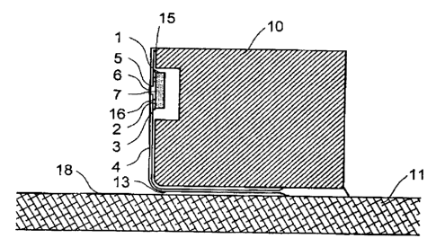
Figure 2 illustrates a module/optical miniature capsule 10
constructed in accordance with the invention and having a
CA 02238754 2005-02-23
WO 97/20344 PCT/SE96/01556
chip-receiving recess portion 14 and guide pins 17 for an
optical fibre connector.
5
r.
Figures 3a-3c illustrate a module/miniature capsule
electrical connection arrangement which includes a soft foil
substrate 9 comprised of a polymeric material, for instance
a polymide, with a metal foil 4, preferably copper foil, on
one side or on both sides of a so-called flex foil. The
copper foil is circuit-printed for the electrical connection
between a chip 1 and a circuit board 11. The chip may be
mounted on the foil substrate 9 by the so-called flip chip
technique, so that the active surfaces 7 of the chip will
face towards the foi2 substrate. The foil substrate has an
opening 5 which lies opposite the active surfaces of the
chip. The bond of the flip chip to the foil substrate can
be further enhanced with the aid of glue 3 which in the
illustrated case may be a transparent glue. The glue may be -
applied so as to fill in the foil opening, either partially
or completely. However, no opening is required when
sufficiently good light transmission is obtained through the
foil substrate_ A thin, transparent and rubbery film 6 can
be applied to the rear side of the foil substrate at
positions corresponding to the positions of the active
surfaces. The foil substrate with holes 8 for receiving
guide pins 17 on the capsule 10 is placed on these pins with
the chip received in the recess 14 in the module/capsule.
The chip and foil substrate can be bonded to the capsule
with glue 15, see Figure 4. when connecting a connector,
the thin, transparent rubbery film 6 will prevent the
formation of an air gap between the connector and the
component. For instance, when the flip chip bumps 2 have a
height of 50-75 urn, the copper foil substrate 4 has a
CA 02238754 1998-05-27
WO 97/20344 PCT/SE96/01556
6
thickness of 10 m, the polymeric foil 9 has a thickness of
25 m, and the film 6 has a thickness of 20 m, the total
distance between the connector fibres and the chip surface
will be 100-130 m, which is considered to be a sufficiently
short distance.
There are, in the main, two ways of achieving electrical
connection between chip and circuit board on the flex foil,
the difference therebetween being governed by the side of the
flex foil on which the conductors 4 lie. If the conductors
lie on the same side as the chip, as in the Figure 3b
illustration, the foil substrate is bent "forwards", see
Figure 4a, and not beneath the capsule when mounting on a
circuit board 11 and is connected with the conductors on the
circuit board 18 either with solder or a conductive glue 13.
If the conductors lie instead on the opposite side to the
chip-mounted side, see Figures 3c, the conductors are bent
beneath the module, see Figure 4b, and connected with the
circuit board mounted conductors with solder or a conductive
glue 13. In this latter case, the chip on one side of the
foil substrate is connected to the conductors on the other
side of the foil substrate through the medium of holes 16.
The active surfaces of the chip can either be positioned
relative to the guide pins in the module as the chip is
placed on the foil substrate or as the foil substrate is
mounted on the module. In the former case, there can be used
a mounting machine capable of placing the chip relative to
the holes 8 with sufficient precision in the order of about 5
m.
CA 02238754 1998-05-27
WO 97/20344 PCTlSE96/01556
7
There may be used a "visual" system that can refer to the
outer edges of the chip or to chip-carried alignment marks
and place these edges or marks correctly in relation to the
holes in the foil substrate. When these holes have the same
diameter as the guide pins 17, the chip will be positioned
correctly in relation to the guide pins when the foil
substrate/chip assembly is fitted onto the pins. In the
latter case, see Figure 5, two of the edges 19, 20 of the
recess 14 have been given sufficient accuracy in relation to
the guide pins 17. The foil substrate/chip assembly is then
fitted onto the guide pins and the outer edges of the chip
pressed against the well-defined edges 19, 20 prior to gluing
the foil substrate/chip assembly. This latter case requires
the holes in the foil substrate 8 to be slightly larger than
the diameter of the guide pins. Instead of using the edges in
the module recess, a metal foil or plastic foil of well-
defined profile can be fitted prior to fitting the foil with
the chip. This foil may also have edges that are well-defined
in relation to said holes, similar to the aforementioned
edges of the module recess and therewith provide well-defined
positioning of the foil substrate/chip assembly.