Note: Descriptions are shown in the official language in which they were submitted.
CA 02238827 1998-OS-27
WO 97/20342 PCT/EP96/05348
1
FORMING CONTACTS ON SEMICONDUCTOR SUBSTRATES FOR
RADIATION DETECTORS AND IMAGING DEVICES
The invention relates to methods of manufacturing radiation detectors and
radiation imaging devices, radiation detectors and imaging devices
manufactured by
these methods and the use of such imaging devices.
A typical method of manufacturing a radiation detector for an imaging device
comprises applying a layer of a metal such as aluminium to both of the main
surfaces
of a planar semiconductor substrate, applying a layer of photoresistive
material to
cover the semiconductor material, exposing the photoresistive material on the
surface
of the planar substrate with an appropriate mask pattern, removing the
photoresistive
material to expose a pattern of the metal to be removed, etching away the
metal to
be removed and then removing the remaining photoresistive material to leave a
pattern of contacts on one surface of the substrate and a metallised layer on
the other
surface of the substrate. The contacts on the first surface of the substrate
then define
an arrangement of radiation detector cells.
For optical wavelengths and charged radiation (beta-rays), silicon has
typically
been used for the semiconductor material for the substrate. A method of the
type
described above has been used to good effect with this material.
in recent years, cadmium zinc telluride (CdZnTe) has increasingly been
proposed as a more suitable semiconductor material for use in X-ray, gamma-ray
and
to a lesser extent beta-ray, radiation imaging. CdZnTe is good at absorbing X-
rays
and gamma-rays giving better than 90% efficiency for IOOkeV X-rays and gamma-
rays with a 2mm thick detector. The leakage or dark current of these detectors
can
be controlled and values of the order of IOnA/cm2 or less at 100Volts bias are
achievable.
A small number of companies worldwide currently produce these detectors
. commercially in a variety of sizes and thicknesses. Usually one or both
sides of the
planar detectors are contacted with a continuous metal layer such as gold (Au)
or
platinum (Pt). As mentioned above, such detector substrates then need to be
<-t -. ~ ...
. . r~-~.4~i. r . : ><,A...i~..l..~.f',I~il-\.~
CA 02238827 2001-12-20
processed to produce a detector having a pattern of contacts (e.g. pixel pads)
on one
surface, with -the opposite surface remaining uniformly metallized, in order
that the
detector may be position sensitive, that is in order that the detector is able
to produce
a detector output indicating- the position at which radiafiion impacts the
detector. A
readout chip then can be 'flip-chip' joined to the patterned side of the
CdZnTe
detector (e.g., by bump bonding using balls of indium or conductive polymer
material, gluing using one-way conductive materials or other conductive
adhesive
Iayer techniques) so that the position dependent electrical signals which
result from
incidence and absorption in the detector cells of X-rays or gamma-rays can be
processed. _ The readout chip could be of the pulse counting type with very
fast
integzation and processing time (typical a few microseconds or at most a few
mill~iseconds)_ Alternatively, it may be, one of type described in. the
Applicant's
~opending Internxtio~al patent application PCT EP95/02056 svhich_ provides for
charge accumulation for individual detector cells. With an imagi.~g device as
1:S described in PCT 1~P95/02056, integration times can be several
milliseconds, or tens
or hundreds .of milli'seconds_ As the signal integration or standby/readout
period
increases it becomes niQre;critical that.:~e gold or platinum contacts on the
CdZnTe
surface are electrically .separated .fo a high degree to avoid signals from
neighbousiag
contacts (pixel pads)' leaking and. rausizig the contrast resolution to
degrade.
It has been found that the traditional method of forming the contacts on the
detector surface, particularly when Cc~mT'e is used as the semiconductor
material,
does not provide as high an electrical separation of the contacts would be
desired to
make optimum use of the advantages ~hxcll are to be derived from the imaging
devices as described in the International application PCT 1rP95/02056.
2-'i
In accordance with one aspect of the invention, there is provided a method of
manufacturing a radiation detector having a plurality of detector cell
contacts on a
first surface of a semiconductor radiation detector substrate at positiorLS
for defining
radiation detector cells and a layer of conductive material on a second
surface of said
3f? substrate opposite to said first surface, said substrate being formed from
cadmium
zinc telluride or cadmium telluride semiconductor material for detecting x-
rays,
gamma-rays or beta-rays, and said cell contacts and sand layer of conductive
material
a CA 02238827 1998-OS-27
3
being on said first and second surfaces, respectively of said semiconductor
material,
wherein said method includes steps of forming said contacts on said first
surface
including steps of:
a) forming layers on said first surface of said substrate with openings to
said
substrate surface at said contact positions, including substeps of:
a(i) forming a layer of passivation material on said first substrate surface;
a(ii) forming a layer of photoresistive material on said passivation layer;
a(iii) selectively exposing said photoresistive material;
a(iv) removing said photoresistive material from areas corresponding to said
contact positions to expose said passivation material layer;
a(v) removing said passivation material from said areas exposed in step
a(iv) corresponding to said contact positions to expose said first
substrate surface.
b) applying metal over said layers) and said openings; and
c) removing metal overlying said at least one layer to separate individual
detector
cell contacts, including substeps of:
c(i) forming a further layer of photoresistive material on at least said
metal;
c(ii) selectively exposing said photoresistive material of said further layer
and removing said photoresistive material of said further layer apart
from areas corresponding generally to said openings;
c(iii) removing metal not covered by said photoresistive material of said
further layer; and
c(iv) removing remaining photoresistive material.
The present inventors have found that the surface resistivity of a CdTe or a
CdZnTe semiconductor substrate is degraded when the substrate is exposed to
metal
etchants suitable for removing gold and/or platinum. As a result of this, the
electrical
separation of the individual contacts which result from the conventional
method of
forming such contacts is not as good as would be expected from the properties
of that
material before treatment. By using a method in accordance with the invention,
the
surface of the semiconductor substrate between the contacts can be isolated
from the
metal etchants, thus preventing the damage which would result if the metal
etchants
A~1IEMDCD' S>-IEET
' CA 02238827 1998-OS-27
4
came into contact with the semiconductor surface.
The use of an insulating layer of passivation material means that after
manufacture of the detector, the passivation material remains between the
contacts
protecting the semiconductor surface from environmental damage in use and
further
enhancing the electrical separation of the contacts.
Preferably, step (a) comprises a further substep:
a(vii) removing remaining photoresistive material of said photoresistive
material layer.
To protect the other main surface and the sides (edges) of the semiconductor
substrate, photoresistive material an additionally be applied to all exposed
surfaces
prior to step a(v).
In a preferred method in accordance with the invention, the areas
corresponding generally to the openings are larger than the corresponding
openings,
so that after the removal in step c(iii) of the metal not covered by the
photoresistive
material of the further layer, the contacts cover the opening and also extend
up and
laterally beyond the opening. In this way the ingress of metal etchant around
the
photoresistive material, whereby the metal etchant might reach the
semiconductor
surface, can be avoided.
The invention finds particular use with substrates formed of cadmium zinc
telluride (CdZnTe).
Preferably, the metal layer for forming the contacts is applied by a method
such as sputtering, evaporation or electrolytic deposition, preferably by
sputtering.
Preferably, the metal layer for forming the contacts comprises gold (Au),
although other metals, for example platinum (Pt) or indium (In), could also be
used.
Step (c) can comprise removing unwanted metal by a photoresist liftoff
technique, although more typically step (c) comprises removing unwanted metal
by
means of an appropriate metal etchant.
Each metal contact can define a respective pixel cell of an array of pixel
cells,
or one of a plurality of strips arranged parallel to each other, depending on
the
application of the detector.
With a method according to the invention, the metal contacts can be of the
order of IO~,m across with a spacing of the order of S~cm.
~','~~~O~D S~~EE
CA 02238827 2001-12-20
The invention further provides a method of manufacturing a radiation imaging
device comprising.
manufacturing a radiation detector as def ned above; and
individually connecting individual contacts for respective detector cells to
5 corresponding circuits on a readout chip, far example by a flip-chip
technique.
In accordance with another a~gect of the invention, there is provided a
radiation detector comprising a semiconductor substrate for detecting
radiation with
a plurality of metal Contacts for respective radiation detector cells on a
first surface
thereof and with a layer of conductive material on a second surface of said
substrate
opposite to said first surface, wherein said substrate 'is fornaed from
cadmium zinc
telluride or cadmium telluride semiconductor material for detecting x-rays,
gamma-
rays or beta-rays,. and said cell contacts and said layer or conductive
material are on
said first and second surfaces, respectively of said semiconductor material,
the overall
width of a said metal contact is larger than the width of said contact
adjacent said
substrate, and aluminium nitride passivation material extends between
individual
contacts and said first surface of said substrate.
In a preferred embodiment of the invention the semiconductor substrate is
made; of cadmium zinc telluride (CdZnTe). Aluminium nitride has been found to
be
paTTicularly effective as a passivation material for CdZnTe because it can be
applied
at low temperature, CdZnTe being temperature sensitive-
~e metal contacts can define an array of pixel cells, or a plurality of strips
arranged parallel to each other, depending on the field of use of the detector-
Pixel contacts formed on detector sulistzate are preferably substantially
circular
and are arranged in a plurality of rows, snore preferably with alternate rows
:?5 preferably being offset from adjacent rows-
The metal contacts are of the order of IO~.m across with a spacing of the
order
of 5~.m_
The resistivity between metal contacts should be in excess of lGit/square,
preferably in excess of lOGS~/square, more preferably in excess of
100Gi1/square and
:30 even more preferably in excess of IOOOGS~/square (XT~/square).
The--metal contacts c~n-compri~:n respective rims upstanriin~
dram the first subscrate su'rfare.
CA 02238827 2001-12-20
5a
.P: radiation imaging device in accordance with the invention finds
particular
CA 02238827 1998-OS-27
. . . .
6 .. ,. .
application for X-ray, gamma-ray and beta-ray imaging.
Thus, an embodiment of the invention can provide a method for
manufacturing, for example, detectors having a CdZnTe substrate with one side
uniformly metallised with gold and the other side patterned with gold
structures in a
manner that does not adversely affect the surface characteristics of the
CdZnTe
substrate between the gold structures. Thus, a method can be provided for
creating
gold structures on one side of a CdZnTe detector, the method achieving inter-
structure resistivity of the order of GS~/square or tens or hundreds of
GS~/square.
The use of an electrically insulating passivation layer between contacts
further
enables the area between metal contacts to be protected, thus giving the
detector
stable performance over time and avoiding effects such as oxidation which
increase
the surface leakage current and decrease the inter-contact resistivity.
Aluminum
nitride (A1N) passivation has been found to be particularly effective when
applied
between gold contacts to protect the surface and enhance the electrical
separation of
the gold contacts. The passivation layer of aluminium nitride can be
implemented at
relatively low temperatures typically less than 100°C. By contrast,
silicon oxide
,. .-:
p,,.;.~;'''. .
CA 02238827 1998-OS-27
7
(Si0=), which is typically used as a passivant for silicon (Si)
semiconductors, needs
temperatures in excess of 200°C. After exposure to these temperatures,
CdZnTe
would be unusable.
Embodiments of the invention will be described hereinafter, by way of
example only, with reference to the accompanying drawings in which:
Figure 1 is an example of a first method of forming metal contacts on a
semiconductor substrate;
Figure 2 is an example of a first method in accordance with the invention of
forming metal contacts on a semiconductor substrate with a passivation layer
between
contacts;
Figure 3 is another example of a second method in accordance with the
invention of forming metal contacts on a semiconductor substrate with a
passivation
layer between contacts;
Figure 4 is a schematic plan view of one contact configuration on a detector
IS substrate;
Figure 5 is a schematic plan view of another contact configuration on a
detector substrate; and
Figure 6 is a schematic plan view of a further contact configuration on a
detector substrate.
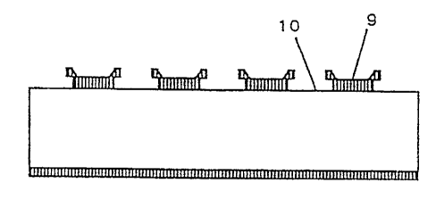
Figure 1 illustrates a method of forming metal contacts on a semiconductor
substrate at positions for defining radiation detector cells. In this example
it is
assumed that the semiconductor substrate is made of cadmium zinc telluride
(CdZnTe), although it will be appreciated that cadmium telluride (CdTe) can be
used.
Also, it will be assumed that the metal used for the metallisation layer and
the gold
contacts is gold, although it will be appreciated that other metals, alloys or
other
conductive materials, for example platinum or indium, could be used.
Thus, Figure 1 is a schematic cross-sectional view from the side of a detector
substrate at various stages in the formation of gold contacts on a CdZnTe
substrate.
Step A: The CdZnTe detector substrate 1 has one face (the lower face in Figure
1) uniformly metallised with gold 2.
Step B: Photoresistive material (photoresist) 3 is spun on the bare face (the
upper face in Figure 1) of the CdZnTe substrate. The photoresist is any of the
CA 02238827 1998-OS-27
WO 97/20342 PCT/EP96/05348
8
common materials used in photolithography, sensitive to certain light
wavelengths for
creating a pattern on it.
Step C: Openings 4 are made in the photoresist using an appropriate mask or
other conventional technique for removing photoresist according to a desired
pattern.
Step D: Photoresist is also applied to the sides 5 of the detector to protect
them
from consequent steps.
Step E: Gold 6 is sputtered, evaporated or laid by electrolysis uniformly over
the photoresist and the openings on the upper side of the detector, as a
result of which
the gold layer 6 covers the photoresist and also contacts the CdZnTe surface
at the
openings of the photoresist. The upper gold surface and the uniformly
metallized
face 2 are electrically separated by the photoresist 5 on the sides (edges) of
the
detector.
Step F: A second layer 7 of photoresist is applied over the gold layer 6 and
also over the uniformly metallized face 2.
Step G: Openings 8 are made in the second layer 7 of photoresist corresponding
to the gold areas that need to be removed, that is the gold areas 8 not in
contact with
the CdZnTe surface. It will be noted that each area of photoresist which
remains on
the upper face is larger than the corresponding area of gold in contact with
the
CdZnTe substrate.
Step H: The unnecessary gold areas 8 are etched away using a gold etchant via
the openings in the second layer ? of photoresist. The second layer of
photoresist 7
protects the gold patterns 9 which are in contact with the CdZnTe surface,
since the
photoresist is not sensitive to the etchant. As the area of photoresist which
remains
on the upper face is larger than the corresponding area of gold in contact
with the
CdZnTe substrate, this prevents the etchant reaching the CdZnTe substrate,
even at
the interface between the gold and the first layer of photoresist 3.
Step I: The second layer 7 of photoresist is removed thus revealing the gold
contacts 9 and the first layer 3 of photoresist is removed thus revealing the
bare face
10 of the CdZnTe detector between the contacts 9. The photoresist layer 5 on
the r
sides of the detector and lower face of the detector is also removed at this
stage. No
photoresist therefore remains on the CdZnTe detector since it is usually
hydroscopic
.x
CA 02238827 1998-OS-27
9
material that in time would absorb humidity and degrade the detector
performance.
Consequently, with the above procedure the end result is a CdZnTe detector
with the lower face 2 uniformly metallised with gold and the upper face
metallized
with gold 9 in a desired pattern. The method ensures that at no stage the gold
etchant
comes in contact with the CdZn'Te surface. The area 10 between the final gold
patterns (pixel pads) 9 thus remains totally unharmed and is not influenced by
the
gold etchant. As a result, the surface of the CdZnTe retains very high
resistivity, in
excess of 1GS2/square between gold pixel pads 9, and very low surface leakage
current. As mentioned above, as high as possible resistivity between gold
pixel pads
9 is desired in order to allow long integration, standby or readout times of
the signal
created from impinging X-rays and gamma-rays without deterioration of the
image
contrast resolution. With the above method, the inter-pixel resistivity can be
tens,
hundreds or even few thousands of GS~/square without compromising pixel
resolution.
Indeed 300GS~/square has been measured and values in excess of a TS~/square
are
achievable.
With the above described method gold pixel pads 9 as small as l0,um across
with S,um spacing in between (i.e. l5um position sensitivity) can be readily
obtained,
while retaining very high inter pixel resistivity.
Additionally, a passivation layer can be applied between the gold pixel pads.
Passivation will ensure a stable performance over time, by avoiding oxidation
of the
surface not covered by gold. Passivation also enhances the inter-pixel
resistivity.
One problem is the compatibility of the passivation layer with respect to
CdZnTe.
The inventors have found that aluminum nitride is an appropriate passivation
material
for CdZnTe.
Figure 2 illustrates a method in accordance with the invention of forming
metal contacts on a semiconductor substrate at positions for defining
radiation detector
cells with a layer of passivation material between the metal contacts. The
same
assumptions are made as for the method of Figure 1. The passivation material
is
aluminium nitride.
Step A: The CdZnTe detector substrate 1 has one face (the lower face in Figure
1) uniformly metallised with gold 2.
CA 02238827 1998-OS-27
Step B: Aluminum nitride 11 is sputtered on the bare face of the CdZnTe
detector 1.
Step C: Photoresistive material (photoresist) 12 is spun on the passivation
layer
11.
5 Step D: Openings 13 are made in the photoresist 12 using an appropriate mask
for removing photoresist according to a desired pattern.
Step E: Photoresist is also applied to the sides 14 of the detector to protect
them from consequent steps.
Step F: Openings 15 are made though the passivation layer 11 using an
10 aluminium nitride etchant to expose the CdZnTe substrate.
Step G: Gold 16 is sputtered, evaporated or laid by electrolysis uniformly
over
the photoresist and the openings on the upper side of the detector, as a
result of which
the gold layer 16 covers the photoresist and also contacts the CdZnTe surface
at the
openings of the photoresist. The upper gold surface and the uniformly
metallized
face 2 are electrically separated by the photoresist 14 on the sides of the
detector.
Step H: A second layer 17 of photoresist is applied over the gold layer 16 and
also over the uniformly metallized face 2.
Step I: Openings 18 are made in the second layer 17 of photoresist
corresponding to the gold areas that need to be removed, that is the gold
areas at 18
not in contact with the CdZnTe surface. It will be noted that each area of
photoresist
which remains on the upper face is larger than the corresponding area of gold
in
contact with the CdZnTe substrate.
Step J: The unnecessary gold areas 19 are etched away using a gold etchant
via the openings 18 in the second layer 17 of photoresist. The second layer of
photoresist 17 protects the gold patterns 20 which are in contact with the
CdZnTe
surface, since the photoresist is not sensitive to the etchant. As the area of
photoresist which remains on the upper face is larger than the corresponding
area of
gold in contact with the CdZnTe substrate, this prevents the etchant reaching
the
CdZnTe substrate, even at the interface between the gold and the first layer
of
photoresist 3.
Step K: The second layer 17 of photoresist is removed thus revealing the gold
' CA 02238827 1998-OS-27
11
contacts 21 and the first layer 12 of photoresist is removed thus revealing
the
passivation layer 11 in the regions 20 between the contacts 21. The
photoresist Layer
on the sides of the detector and lower face of the detector is also removed at
this
stage. No photoresist therefore remains on the CdZnTe detector since it is
usually
hydroscopic material that in time would absorb humidity and deteriorate the
detector
performance.
Once again, at no step does the gold etchant, or indeed the aluminium nitride
etchant come in contact with the regions 20 between the gold pixel contacts 21
or the
edges and sides of the CdZnTe detector. As a consequence, during the above
procedure the surface of the substrate at 20 between the gold contacts 21
remains
unharmed, retaining very high resistivity of the order of GS2/square, tens,
hundreds
or even thousands of GS2/square. The aluminum nitride passivation covers the
area
between the metal contacts 21 protecting the corresponding regions form
oxidation
(providing stability over time) and enhancing the inter-contact resistivity.
1~ Variations of the above procedure may be applied without departing from the
scope of the invention. For example the first layer 12 of photoresist may be
removed
prior to gold sputtering (after openings 15 have been made). This alternative
method
of the invention is shown in Figure 3. In the method shown in Figure 3, steps
A -
F correspond to steps A - F of the method of Figure 2.
20 Step G: This is an additional step in which the photoresist is removed from
the
upper face to expose the passivation layer at 22.
Step H: This corresponds generally to step G of Figure 2 except that in step H
the gold is applied over the passivation layer at 22 and the openings at 23
(see Figure
3G).
Steps I - L correspond generally to steps H - K, respectively, of Figure 2,
except for
the absence of the layer of photoresist 12.
CA 02238827 1998-OS-27
WO 97120342 PCT/EP96/05348
12
A result of the method of Figure 3 is that the resultant pixel pads are
flatter
(i.e. they have a lower profile) than with the method of Figure 2, as can be
seen by
comparing Figures 2K and 3L.
Figures 4, 5 and 6 are used to illustrate possible pixel contact patterns on
the
upper surface of the detector substrate. In Figure 4, an array of square pixel
contact
pads is shown. In Figure 5 an array of circular pixel pads is shown. The use
of
circular rather than square pixel pads increases the surface resistance
between pads
by increasing the amount of resistive material between adjacent pads. Figure 6
illustrates an array of offset (honeycombed) pixel pads. Once again this
further
increases the resistance between pads by increasing the surface amount of
resistive
material between adjacent pads.
It will be appreciated that rather than providing an array of contacts for
defining an array of pixel detector cells, other contact configurations, for
example
contact strips for defining strip-shaped detector cells, can be obtained with
the same
method.
Although reference has been made to the use of gold for the contacts, gold is
an advantageous material because it can be readily etched to define the
desired contact
structures and give good contact {better than aluminium, for example) to the
CdZnTe,
it is apparent that the procedure disclosed above could also be applied for
any kind
of metal contacts (e.g. platinum) in combination with an appropriate etchant.
As mentioned above, it should be noted that the longitudinal dimensions
{width) of the top of the gold contacts 9 (Figure 1), 21 (Figure 2) or 32
(Figure 3)
is larger than that at the gold-substrate interface. This arises from the
relative sizes
of the openings to the substrate surface and the photoresist left over the
portions for
forming the contacts to ensure that, when redundant gold is etched away, the
etchant
will not seep through to the interface between first layer of photoresist (or
the
passivation layer} and gold in the openings.
A radiation imaging device can be constricted by connecting a radiation
detector produced by the method according to one of the above described
methods to -
a readout chip having circuits for accumulating charge from successive
radiation hits,
individual contacts (e.g. pixel pads) for respective detector cells being
'flip-chip'
F ~ h y~' ~ ~~. ' r u-~.l ~~ ~.i Y t '~=
~~..~~i~ ' -
r
CA 02238827 2001-12-20
w v r ucv.a4~ PCT/EP9G/05348
13
joined (e.g. , by bump bonding using balls of indium or conductive polymec
material,
gluing using one-way conductive materials, yr other cot~duetive adhesive layec
techniques) to respective circuits for accumulating charge.
Thus, the invention teaches how to obtain a radiation detector (e_g. based on
a CdZnTe substrate) with one side metaltised according to a desired pattern
with
maximum possible electrical resistivity separation between the metal contacts_
High
resistivity between mesa! concocts is desirable to improve conaast resolution.
and
eliminate signal leakage between 'adjacent metal contacts on the substrate
surface.
Tlzis is particularly retevant when long charge accumulation times and lvag
standby/readout times are employed by the readout clop. ouch accumulation and
scandbylreadout times could, for example, be in excess of lmsec in examples of
imaging devices using a radiation detector marrufaccured itt accordance with
the
ptrsent invention. Such im$ging devices find application, for e~cample, foe X-
toy.
gamma-ray and beta-ray imaging as described in the applicant's International
patEnt
applicatiotr PCT EP95/02056..~ - .
Although particular embodiments of tb~e invention have been described by way
of example, it wilt be 'appreciated chat additions, modifications anCl
alternatives thereto
nnay 6e envisaged.