Note: Descriptions are shown in the official language in which they were submitted.
CA 02238955 1998-OS-26 617PO1CA
NOVEL BIASING SCHEME FOR GAASFET AMPLIFIER
1 Introduction:
GARS and PHEMPT GAAS transistors are now widely used for low noise amplifiers
(LNA's) in at frequencies in excess of 1 GHz. Such devices are relatively low
cost and
offer very low noise and high gain at moderate currents and voltages.
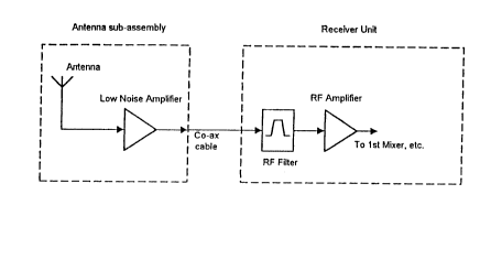
When such amplifiers are used as the first receiver block to amplify signals
received at
microwave antennas, it is common to use 2 or more stages, frequently with anti-
aliasing
filters included in the amplifier chain, as shown in fig 1 a and 1 b
Generally, the LNA block is wideband relative to the signal bandwidth and
usually does
not impose any limitation on signal modulation or architecture of the balance
of the
receiver system. For example, such an LNA could be used for a narrow band QPSK
system or for a wideband direct sequence spread spectrum system, provided only
that
any in-line filters have sufficient bandwidth to pass the entire signal
spectrum (as is the
usual case).
The power consumption of the individual stages of such amplifiers is typically
10mA
from a 5V supply, and multiple stages increase the current draw
proportionally. While
this power current is moderate compared with earlier technology, it represents
a
substantial drain for battery powered equipment such as hand held global
positioning
system (GPS) receivers. There is thus benefit to be derived from a further
reduction in
the current consumption.
2 Biasing considerations.
A PHEMPT transistor, when operated at drain current of 10mA, has a negative
gate to
source voltage typically between 0.1 V and 0.4V. If the source of grounded, it
is thus
necessary to bias the gate negatively with respect to ground to achieve the
desired
bias current. This is commonly achieved by the use of capacitive pump circuits
which
generate negative bias voltages. The PHEMPT gate input impedance (at DC) is
very
high and thus the input bias current is very low and the bias circuit current
consumption
can be made relatively low.
The variation in the Source to Gate threshold for GARS FET transistors is not
well
controlled and consequently. additional control circuitry is required to
regulate the bias
current which flows in the e~rcuit.Commonly, the negative bias voltage
provided by
the capacitive pump circuit simply provides the necessary biasing voltages and
additional circuitry is required to implement the bias current control.
Fig 2a shows a means of biasing a PHEMPT without a negative bias pump. This
relies
upon a degeneration resistor in the source to control the bias current. A
major
disadvantage of this simple circuit is that the variation in gate threshold
for PHEMPT
devices is very poor leading to wide tolerances in current draw.
Fig 2b shows a biasing circuit which makes use of a negative bias device.
CA 02238955 1998-OS-26
PHEMPT and GAASFET transistors are capable of operation at extremely high
frequencies, and it is important to provide well controlled AC source
impedances at all
ports up to the maximum frequency of operation to prevent spurious
oscillations. It is a
common practice to directly connect the GARS FET source to ground plane to
achieve
such control.
3 The improved biasing system.
If great care is paid to the PHEMPT source decoupling to make the it stable,
it is then
possible to bias the source to an arbitrary DC potential. This then allows the
DC path to
be separated from the AC path and a circuit can be devised in which the bias
current in
a second stage also flows in the first stage, thereby halving the current
requirements.
This is shown symbolically in Fig 3.
However, it is still necessary to control the current by a negative feedback
loop, and
this is shown symbolically in Fig 4. A bipolar transistor (Q3) acts as a
constant current
sink and thus its collector current defines the source to drain current in Q1.
This bias
current is sensed in a series resistor (R3) in the current path. In order to
establish the
correct biases on the two transistors, the gate bias of Q2 is defined by the
potential
divider R6, R7. This then determines the source potential of Q2 to be Vt (for
Q2) above
the Q2 gate potential. By these means the supply voltage may be "split" across
Q1 and
Q2.
L2 acts as an RF choke and serves to separate the AC and DC paths. L1 and C2
provide AC matching from the PHEMPT output to the F1 filter input. R2 is a
stabilising
resistor which plays no active role in the biasing (since at low frequencies,
the drain of
QZ provides a constant current output):
The potential across R3 is made equal to the potential across R4 which is
established
by the R4 R5 potential divider. By inspection it can be seen that if the
current in the
sense resistor is low compared with that defined by the potential divider, the
base of
the NPN transistor is driven more positive (to increase the current) and vice
versa. By
these means the current in both the upper and lower transistors is defined by
a
single loop and the current is "used" twice.
The minimum drain to source voltage required for GAASFET or PHEMPT transistors
(to
maintain both a low noise figure and high gain) is lower than 1 V so that it
is possible to
"fit" the whole circuit into 2.7V, provided the sensing operational amplifier
is capable of
operation from a single low voltage supply. Such amplifiers are commonly
available.
Since it is common for amplifiers to packaged as pairs, a second amplifier can
be used
to bias the gate of the second stage transistor Q2. This is shown in Fig 5
which also
shows the RF components used to implement this particular version of the LNA.
The biasing circuit is inherently stable at low frequencies and bias
stabilisation is not
required.
2
CA 02238955 1998-OS-26
4 The advantages of this improved biasing circuit are:
4.1 Only one negative feedback stage is necessary to establish the bias
current in
both a first stage and a second stage of a low noise amplifier.
4.2 The available supply voltage is "shared" between the transistors in the
two
stages, resulting in a very low drop-out voltage.
4.3 The bias current is "used" twice resulting in current consumption half of
that
which would be required for a conventional circuit.
4.4 The negative gate threshold of Q1 allows the gate of Q1 to be biased at
ground,
which still provides sufficient "voltage headroom" for Q3 to act as a constant
current
sink.
4.5 A single control node provides for power down of both stages of the LNA
(for
power saving applications).
4.6 The bias control is extremely precise because it is solely determined by
resistor
values and is independant of PHEMPT parametric variation.
Other Variants
It is possible to combine the key elements of this biasing system with a
conventional
negative bias pump circuit. This is shown in Fig 6. In this, a capacitive pump
is used
to generate a negative bias voltage on the gate of the 1st amplifier
transistor, Q1,
which then provides the constant current sink function provided by Q3 shown in
figures
4 and 5. The example in fig 6 is functionally equivalent to those in figures 4
and 5, but
offers some advantages:
5.1 The source of Q1 is tied directly to ground, eliminating the requirement
for
bipass capacitors, and simplifying the stablity requirements
5.2 The NPN bias transistor (Q3 above) is eliminated.
6 Integrated Circuit bias systems.
Both the ground bias (the first version) and the negative bias versions are
very
convenient to integrate, where advantage can be taken of bandgap voltages and
additional amplifiers.
It is possible to configure the circuit so that the bias current is determined
as a function
of a band gap voltage divided by a resistor.
In figure 7, the amplifier bias current flows through R5, and the magnitude
sensed by
the potential across it. Amplifier A1 combined with R6, R7, R8, and R9 serve
as a
CA 02238955 1998-OS-26
differential amplifier which generates an output proportional to the potential
across R5,
but with respect to ground.
The output of a very low current band gap voltage generator is input to the
potential
divider R2, R3 and this provides a reference input to A2. The sense of the
feed back is
so as to make the output of A1 track the reference input to A2. By these
means, the
PHEMPT bias current is determined by a ratio which is essentially a supply
voltage and
temperature independent. It is envisioned that the current determining
resistor (R5)
would be discrete, thereby making the bias current largely independent of both
supply
voltage and temperature, within a wide range. Thus the current consumption
with a 5V
supply is thus virtually the same as that at 3V.
The negative charge pump version may be combined with the bandgap biasing to
achieve the same end result. Either version are very suitable for integration.
4