Note: Descriptions are shown in the official language in which they were submitted.
CA 02238974 1998-0~-28
E2927
59/25
DESCRIPTION
METHODS OF PROCESSING SEMICONDUCTOR WAFER AND
PRODUCING IC CARD, AND CARRIER
TECHNICAL FIELD
The present invention relates to semiconductor
wafer processing techniques, and particularly to a
technique effective for use in handling semiconductor
wafers when the semiconductor wafers are processed to a
very small thickness of 100 ~m or below.
BACKGROUND ART
Now, in the semiconductor devices required to
be thin as well as high density and small size, such as
semiconductor devices applied to IC cards, thinner
packages than the usual ones are used, such as TQFP
(thin quad flat package) and TSOP (thin small outline
package). In order to manufacture such packages, it is
necessary to make the semiconductor wafers particularly
thin. Here, the known techniques for making the
semiconductor wafers thin, as for example described in
"PRACTICAL LECTURES VlSI PACKAGING TECHNOLOGY (the
second volume)" published by NIKKEI BP Co.,Ltd. on May
31, 1993, pp. 12 to 14, are three types of grinding,
chemical etching and lapping. As in the publication,
the grinding is the technique for grinding the rear
surface of a semiconductor wafer with a diamond
grindstone, the etching is the technique for etching the
CA 02238974 1998-0~-28
rear surface of a semiconductor wafer with a mixture of
chiefly fluoric acid and nitric acid while the
semiconductor wafer is being rotated with high speed,
and the lapping is the technique for grinding the rear
surface of a semiconductor wafer with abrasive grains.
The thinning process by the grinding or
lapping is able to grind semiconductor wafers of general
thickness, or about 625 ~m (or 725 ~m) to a thickness of
about 300 ~m, but has a difficulty when trying to grind
to a thickness of, for example, 100 ~m or below because
the semiconductor wafer might be cracked even under
strict care when removing it from the grinder. Even if
the wafer is not cracked, it is remarkably warped
depending on the stress in the passivation film on the
wafer surface and the internal stress of the wafer.
This warp causes operational problems in the following
processes such as dicing. In addition, it is difficult
to process large-diameter semiconductor wafers, or
12-inch or above wafers to a specified level of flatness
and uniformity.
Moreover, in the thinning process by etching,
since the wafer is rotated at high speed, an excessive
stress is exerted on the semiconductor wafer by the pins
that hold its outer peripheral portion at a plurality of
locations, thus breaking the wafer. Furthermore, a warp
will occur due to the internal stress as in the grind-
ing.
In order to solve the above problems, the
CA 02238974 1998-0~-28
inventors have found to fix the semiconductor wafer to a
certain support base with tape and process it after
various examinations. However, normal tape is also
discarded after use in the process of each wafer, thus
increasing the cost, or causing a new problem.
Accordingly, it is an object of the invention
to provide a technique capable of making semiconductor
wafers thin without any crack by solving the above
technical problems.
It is another object of the invention to
provide a technique capable of making semiconductor
wafers thin under easy operation.
It is still another object of the invention to
provide a technique capable of making semiconductor
wafers thin without any warp.
It is further object of the invention to
provide a technique capable of making semiconductor
wafers thin at low cost.
The features of the invention, and the above
objects of the invention together with other objects
will be best understood by the following description,
taken in conjunction with the accompanying drawings.
DISCLOSURE OF INVENTION
A typical one of the inventions disclosed in
this application will be described briefly as below.
The semiconductor wafer processing method
according to the invention includes a first step of
CA 02238974 1998-0~-28
preparing a plate-like or film-shaped carrier that is
formed of a base and an adhesive member provided on one
surface of the base, a second step of producing a wafer
composite by bonding a semiconductor wafer to the
carrier in such a manner that the rear surface of the
wafer with no circuit elements formed therein is
opposite to the carrier, and a third step of making the
semiconductor wafer thin by spin-coating an etchant on
the rear surface of the semiconductor wafer of the wafer
composite that is supported with its semiconductor wafer
side up.
In this semiconductor wafer processing method,
the semiconductor wafer of the wafer composite is made
to have a larger diameter than the carrier so that all
the outer peripheral edge of the semiconductor wafer
overhangs from the carrier when the wafer composite is
formed by bonding the wafer on the carrier. In the
third step, the semiconductor wafer can be thinned while
a gas is being blown from below against the wafer
composite. In addition, the semiconductor wafer may be
made to have a diameter equal to or smaller than the
carrier so that the peripheral edge of the wafer does
not overhang from the carrier when the wafer composite
is formed.
Moreover, after the semiconductor wafer is
thinned by the third step, a fourth step and a fifth
step may be provided. The fourth step is for sticking
the rear side of the wafer on a dicing sheet and peeling
CA 02238974 1998-0~-28
off the carrier, and the fifth step is for dicing the
semiconductor wafer on the dicing sheet into individual
semiconductor chips.
The semiconductor wafer processing method of
the invention includes a first step of preparing a
semiconductor wafer with a passivation film formed on
its main surface in which circuit elements are already
built, a second step of preparing a plate-like or
film-like carrier that is formed of a base and an
adhesive member provided on one surface of the base, a
third step of producing a wafer composite by bonding the
semiconductor wafter to the carrier in such a manner
that the rear surface of the wafer with no circuit
elements formed therein is opposite to the carrier, and
a fourth step of holding the wafer composite with its
semiconductor wafer side up and spin-coating an etchant
on the rear surface of the semiconductor wafer thereby
to thin the semiconductor wafer. In this case, after
thinning the semiconductor wafer at the fourth step, it
is possible to add a fifth step of attaching the rear
surface of the semiconductor onto a dicing sheet and
peeling off the carrier from the wafer composite, and a
sixth step of dicing the semiconductor wafer left on the
dicing sheet into individual semiconductor chips.
The IC card producing method according to the
invention includes a first step of preparing a
plate-like or film-like carrier that is formed of a base
and an adhesive member provided on one side of the base,
CA 02238974 1998-0~-28
a second step of producing a wafer composite by bonding
a semiconductor wafer to the carrier in such a manner
that the rear surface of the wafer with no circuit
elements formed therein is opposite to the carrier, a
third step of holding the wafer composite with its
semiconductor wafer side up and spin-coating an etchant
on the rear surface of the semiconductor wafer thereby
to thin the semiconductor wafer, a fourth step of
attaching the thinned rear surface of the semiconductor
wafer to a dicing sheet and peeling off the carrier from
the wafer composite, a fifth step of dicing the semicon-
ductor wafer left on the dicing sheet into individual
semiconductor chips, a sixth step of reducing or loosing
or losing the adhesion of the dicing sheet, a seventh
step of mounting one or ones of the semiconductor chips
on a card substrate at chip-mounting positions, and an
eighth step of producing an IC card by using the card
substrate with the semiconductor chip or chips mounted.
According to the invention, there is provided
an IC card producing method including a first step of
preparing a semiconductor wafer with a passivation film
formed on its main surface in which circuit elements are
already built, a second step of preparing a plate-like
or film-like carrier that is formed of a base and an
adhesive member provided on one surface of the base, a
third step of producing a wafer composite by bonding a
semiconductor wafer to the carrier in such a manner that
the rear surface of the wafer with no circuit elements
CA 02238974 1998-0~-28
formed therein is opposite to the carrier, a fourth step
of holding the wafer composite with its semiconductor
wafer side up and spin-coating an etchant on the rear
surface of the semiconductor wafer thereby to thin the
semiconductor wafer, a fifth step of attaching the
thinned rear side of the semiconductor wafer to a dicing
sheet and peeling off the carrier from the wafer
composite, a sixth step of dicing the semiconductor
wafer left on the dicing sheet into individual semicon-
ductor chips, a seventh step of reducing or loosing orlosing the adhesion of the dicing sheet, an eighth step
of mounting one or ones of the semiconductor chips on a
card substrate at chip-mounting positions, and a ninth
step of producing an IC card by using the card substrate
with the semiconductor chip or chips mounted.
When bumps are formed at the chip electrodes
of the semiconductor wafer in the IC card producing
methods of the invention, the thickness of the adhesive
member provided on the base should be equal to or larger
than the height of the bumps. In addition, at the
seventh step, it is desirable to directly mount the
semiconductor chips on the card substrate from the
dicing sheet.
Moreover, the carrier in the invention is used
in the semiconductor wafer processing method, and its
adhesive member comprises an elastically flexible
suction pad for sucking the semiconductor wafer by
vacuum. In this carrier, the suction pad may have a
CA 02238974 1998-0~-28
size enough to suck substantially all region of one
surface of the semiconductor wafer. In addition, it may
be formed in a ring shape along the outer periphery of
the semiconductor wafer. Also, a plurality of such
suction pads may be provided on all the region of one
surface of the base in order to hold the semiconductor
wafer at a plurality of locations.
In addition, the carrier in the invention is
used in the semiconductor wafer processing method, and
its adhesive member comprises a suction groove that is
formed in the base to be communicated with a vacuum hole
connected to a vacuum pump so that the semiconductor
wafer is sucked by vacuum and peeled off from the
carrier by restoring to atmospheric pressure.
Also, the carrier in the invention is used in
the semiconductor wafer processing method according to
the invention, and its adhesive member is constituted by
a plurality of suction holes which are formed in one
surface of the base at different locations to be
communicated with a vacuum hole connected to a vacuum
pump so that the semiconductor wafer is sucked by
negative pressure and peeled off from the carrier by
restoring to atmospheric pressure.
Moreover, the carrier in the invention is used
in the semiconductor wafer processing method according
to the invention, and its adhesive member comprises a
porous member that has a great number of small holes and
is provided on one surface of the base for the small
CA 02238974 1998-0~-28
holes to be communicated with a vacuum hole connected to
a vacuum pump so that the semiconductor wafer is sucked
by vacuum and that it is peeled off from the carrier by
restoring to atmospheric pressure.
Also, the carrier in the invention is used in
the semiconductor wafer processing method according to
the invention, and its adhesive member includes an
exfoliation portion coplanar with the base to form a
plurality of small recesses, and gelled silicone
interposed between the peeling portion and the
semiconductor wafer to make the base adhere to the
semiconductor wafer, whereby when the surroundings of
the exfoliation portion are evacuated the silicone is
sunk in the recesses so as to be peeled off from the
semiconductor wafer. The exfoliation portion of the
carrier may be a net or an irregular surface formed on
the base.
In addition, the carrier employed in the
semiconductor wafer processing method according to the
invention has its base made of a transparent material
and its adhesive member made of a W cure-type adhesive
of which the adhesion is reduced or lost by ultraviolet
rays radiated through the base so that the carrier can
be peeled off from the semiconductor wafer.
Also, the adhesive member employed in the
semiconductor wafer processing method according to the
invention is made of a temperature activation type
adhesive of which the adhesion is reduced or lost by
CA 02238974 1998-0~-28
temperature change so that the carrier can be peeled off
from the semiconductor wafer. The temperature activa-
tion type adhesive of this carrier may have such a
characteristic that its adhesion is reduced or lost at a
low temperature.
The adhesive member employed in the semi-
conductor wafer processing method according to the
invention is a liquid that acts as an adhesive in such a
manner that the semiconductor wafer and the base are
made in intimate contact with each other by the
interfacial force exerted therebetween and that the
semiconductor wafer is peeled off from the base by
ultrasonic waves.
The base of the carrier should be made of an
acid-resistant material, for example, compacted fibrous
fluororesin.
Thus, since the semiconductor wafer thinning
process is performed on the wafer composite formed by
bonding the semiconductor wafer to the carrier, any
cracks can be prevented from occurring even with no
strict care when the semiconductor wafer is thinned. In
addition, since the reduction of the rigidity of the
thinned semiconductor wafer can be compensated for by
the carrier so that release of the stress in the
passivation film is prevented, the semiconductor wafer
is not warped. Thus, the semiconductor wafer can be
stably processed to be extremely thin.
Moreover, since the wafer composite can be
CA 02238974 1998-0~-28
handled in the same way as the semiconductor wafer
having a normal thickness before thinning, any cracks
can be prevented form occurring on the semiconductor
wafer even with no strict care, and the work for
thinning can be made with ease.
In addition, since the carrier of the wafer
composite is supported so that no unnecessary stress is
exerted on the semiconductor wafer, any warp does not
occur, and thus the semiconductor can be thinned with
high quality.
If the semiconductor wafer is fixed to the
base by the suction pad, the carrier is not necessary to
be discarded after use, and can be simplified in its
construction, and thus the semiconductor wafer can be
thinned at low cost.
If the wafer composite is formed by attaching
the semiconductor wafer to the base to overhang from the
carrier and spin-coated with an etchant while gas is
continuously blown against this wafer composite, the
etchant can be surely prevented from flowing around the
outer peripheral side into the main surface, thus the
circuit elements being not damaged.
If the wafer composite is so formed that the
outer periphery of the semiconductor wafer does not
overhang from the carrier, the etchant is prevented from
flowing around the peripheral side into the main
surface, and thus it is not necessary to blow gas
against the wafer composite. Moreover, since the
CA 02238974 1998-0~-28
thinned semiconductor wafer does not overhang from the
carrier, the wafer composite can be easy to handle.
Also, since all the main surface of the semiconductor
wafer is covered by the carrier so that it is shielded
from the external atmosphere, the rear surface of the
semiconductor wafer can be etched even by dipping.
If an IC card is produced by using semi-
conductor chips that are produced by dicing the thinned
semiconductor wafer, the IC card can be made thinner
than that of the conventional one.
If the thickness of the adhesive member
provided on the base is made equal to or larger than the
height of the bumps formed on the semiconductor wafer,
all the carrier is made in intimate contact with the
semiconductor wafer so that both are not peeled off from
each other. Also, if the semiconductor chips are
directly mounted on the card substrate from the dicing
sheet, the additional moving operation for the semi-
conductor chips can be omitted, thus throughput can be
improved.
The peeling operation after thinning can be
simplified by taking the vacuum suction structure of the
carrier for sucking the semiconductor wafer or by using
the adhesive member formed of the peeling portion and
the adhesive sheet or formed of W cure-type adhesive or
temperature activation adhesive. Moreover, since the
semiconductor wafer is always kept flat along the base,
the warp of the semiconductor wafer can be effectively
CA 02238974 1998-0~-28
suppressed.
Since the carrier formed of an reversible
temperature activation type adhesive can be repeatedly
used in the thinning process, the thinned semiconductor
wafer can be mass-produced at low cost.
Since the carrier having the base made of an
acid resistant material can be repeatedly used in the
thinning process, the thinned semiconductor wafer can be
mass-produced at low cost.
Since the base may be made of compacted
fibrous fluororesin having a feature of resistance
against acid, it is possible to use various different
adhesives such as temperature activation type adhesive
with weak adhesion to the base.
BRIEF DESCRIPTION OF DRAWINGS
Fig. 1 is a plan view of the carrier used in
the semiconductor wafer thinning process of one
embodiment of the invention, Fig. 2 is a cross-sectional
view taken along a line II-II in Fig. 1, Fig. 3 shows
part of the semiconductor wafer processing procedure
using the carrier of Fig. 1, Fig. 4 is another part of
the procedure using the carrier of Fig. 1 after the
operation of Fig. 3, Fig. 5 is a schematic diagram of
the etching apparatus used in the semiconductor wafer
thinning process according to the invention, Fig. 6
shows another part of the procedure using the carrier
after the operation of Fig. 4, Fig. 7 shows another part
CA 02238974 1998-0~-28
14
of the procedure using the carrier after the operation
of Fig. 6, Fig. 8 shows another part of the procedure
using the carrier of Fig. 1 after the operation of Fig.
7, Fig. 9 shows another part of the procedure using the
carrier of Fig. 1 after the operation of Fig. 8, Fig. 10
shows another part of the procedure using the carrier of
Fig. l after the operation of Fig. 9, Fig. 11 is a plan
view of the carrier used in the semiconductor wafer
thinning process according to another embodiment of the
invention, Fig. 12 is a cross-sectional view taken along
a line XII-XII in Fig. 11, Fig. 13 is a plan view of the
carrier used in the semiconductor wafer thinning process
according to still another embodiment of the invention,
Fig. 14 is a cross-sectional view taken along a line
XIV-XIV in Fig. 13, Fig. 15 is a plan view of the
carrier used in the semiconductor wafer thinning process
according to still another embodiment of the invention,
Fig. 16 is a cross-sectional view taken along a line
XVI-XVI in Fig. 15, Fig. 17 is a plan view of the
carrier used in the semiconductor wafer thinning process
according to still another embodiment of the invention,
Fig. 18 is a cross-sectional view taken along a line
XVIII-XVIII in Fig. 17, Fig. 19 is a plan view of the
carrier used in the semiconductor wafer thinning process
according to still another embodiment of the invention,
Fig. 20 is a cross-sectional view taken along a line
XX-XX in Fig. 19, Fig. 21 is a plan view of the carrier
used in the semiconductor wafer thinning process
CA 02238974 1998-0~-28
according to still another embodiment of the invention,
Fig. 22 is a cross-sectional view taken along a line
XXII-XXII in Fig. 21, Fig. 23 shows part of the
semiconductor wafer processing procedure using the
carrier of Fig. 21, Fig. 24 shows another part of the
semiconductor wafer processing procedure using the
carrier of Fig. 21 after the operation of Fig. 23, Fig.
25 shows another part of the semiconductor wafer
processing procedure using the carrier of Fig. 21 after
the operation of Fig. 24, Fig. 26 shows another part of
the semiconductor wafer processing procedure using the
carrier of Fig. 21 after the operation of Fig. 25, Fig.
27 shows another part of the semiconductor wafer
processing procedure using the carrier of Fig. 21 after
the operation of Fig. 26, Fig. 28 shows another part of
the semiconductor wafer processing procedure using the
carrier of Fig. 21 after the operation of Fig. 27, Fig.
29 (a) illustrates the state of the bonded semiconductor
wafer and carrier, Fig. 29 (b) illustrates the state of
the separated semiconductor wafer and carrier, Fig. 30
shows another part of the semiconductor wafer processing
procedure using the carrier of Fig. 21 after the opera-
tion of Fig. 28, Fig. 31 shows part of the semiconductor
wafer processing procedure according to still another
embodiment of the invention, Fig. 32 shows another part
of the procedure after the operation of Fig. 31, Fig. 33
shows another part of the procedure after the operation
of Fig. 32, Fig. 34 shows another part of the procedure
CA 02238974 1998-0~-28
16
after the operation of Fig. 33, Fig. 35 shows another
part of the procedure after the operation of Fig. 34,
Fig. 36 shows another part of the procedure after the
operation of Fig. 35, Fig. 37 shows another part of the
procedure after the operation of Fig. 36, Fig. 38 is a
plan view of the carrier used in the semiconductor wafer
thinning process according to still another embodiment
of the invention, Fig. 39 is a cross-sectional view
taken along a line XXXIX-XXXIX in Fig. 38, Fig. 40 is a
cross-sectional view of the carrier used in the semi-
conductor wafer thinning process according to still
another embodiment of the invention, Fig. 41 shows part
of the semiconductor wafer processing procedure accord-
ing to still another embodiment of the invention, Fig.
I5 42 shows another part of the procedure following the
operation of Fig. 41, Fig. 43 shows another part of the
procedure following the operation of Fig. 42, Fig. 44
shows another part of the procedure following the
operation of Fig. 43, Fig. 45 shows another part of the
procedure following the operation of Fig. 44, Fig. 46
shows another part of the procedure following the
operation of Fig. 45, Fig. 47 shows another part of the
procedure following the operation of Fig. 46, Fig. 48
shows another part of the procedure following the
operation of Fig. 47, Fig. 49 shows another part of the
procedure following the operation of Fig. 48, Fig. 50
shows another part of the procedure following the
operation of Fig. 49, Fig. 51 shows another part of the
CA 02238974 1998-0~-28
procedure following the operation of Fig. 50, Fig. 52
shows another part of the procedure following the
operation of Fig. 51, Fig. 53 shows another part of the
procedure following the operation of Fig. 52, Fig. 54
shows another part of the procedure following the
operation of Fig. 53, Fig. 55 is an enlarged plan view
of the chip electrode portion of the semiconductor wafer
of Fig. 41, Fig. 56 is a cross-sectional view taken
along a line C1-Cl, Fig. 57 shows the details of Fig. 48,
Fig. 58 is a plan view of the internal structure of the
IC card produced according to this embodiment, Fig. 59
is a cross-sectional view taken along a line C2-C2, Fig.
60 is an enlarged cross-sectional view of portion A of
Fig. 59, and Fig. 61 is an enlarged cross-sectional view
of portion B of Fig. 60.
BEST MODE FOR CARRYING OUT THE INVENTION
Preferred embodiments of the invention will be
described in detail with reference to the accompanying
drawings. In all the figures useful for the embodi-
ments, like elements are identified by the samereference numerals, and will not be repeatedly
described.
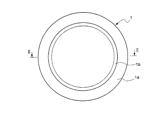
Fig. 1 is a plan view of the carrier used in
the semiconductor wafer thinning process according to
one embodiment of the invention, Fig. 2 is a cross-
sectional view taken along the line II-II in Fig. 1,
Fig. 3, Fig. 4 and Figs. 6 to 10 are flow diagrams of
CA 02238974 l998-0~-28
18
the semiconductor wafer processing procedure using the
carrier of Fig. 1, and Fig. 5 is a schematic diagram of
the etching apparatus used in the semiconductor wafer
thinning process.
The carrier 1 depicted in Figs. 1 and 2 has a
plate-like shape in order for the semiconductor wafer 2
(shown in Fig. 3 and other figures) to be stuck and held
on the carrier to form the wafer composite 10 (as shown
in Fig. 3 and other figures). This carrier 1 is formed
of a base la and an elastically flexible suction pad
(adhesive member) lb provided on one surface of the base
la. The base la formed in a disk along the shape of the
semiconductor wafer 2 is made of, for example,
fluororesin, glass plate or epoxy resin which has
resistance to acid. The suction pad lb to which the
semiconductor wafer 2 is stuck is made of, for example,
soft rubber having a size enough to absorb, or adhere to
substantially all region of one surface of the semicon-
ductor wafer 2. In this embodiment and the following
embodiments, the base la constituting the carrier 1 is
preferably made of a material having resistance to acid
as described above in order that it can be prevented
from changing in quality by an etchant L (Figs. 5, 6).
In addition, in order that the semiconductor wafer 2 can
be prevented from being broken by the action of
concentrated stress by the supporting pins of the
etching apparatus on the supported locations of the
semiconductor wafer 2 as will be described later, the
CA 02238974 1998-0~-28
diameter of the base la is designed to be slightly, for
example, about 10 ~m larger than the semiconductor wafer
2.
The semiconductor wafer 2 stuck on the suction
pad lb is ground to be thin by the following process.
First, the rear surface of the semiconductor
wafer 2, after the completion of the pretreatment
process up to the electric examination for the circuit
elements formed on the main surface, is ground to a
thickness of, for example, about 250 ~m with a diamond
grindstone or abrasive grains. In this case, immediate-
ly the thinning process described later may be performed
without this preliminary process.
Then, the semiconductor wafer 2, under the
condition that its rear surface having no circuit
elements is directed to the outside, or opposite to the
carrier l, is pressed against the carrier l as shown in
Fig. 3. When a light weight is loaded uniformly on the
entire surface of the semiconductor wafer 2, the suction
pad lb is elastically deformed so that the volume of the
pad closed by the wafer 2 is decreased to discharge the
internal air. When the load is removed from the wafer
2, the adhesion pad lb intends to be restored by itself
to the original shape. As a result, the reduced volume
expands somewhat close to the original volume, but air
is prevented from flowing into the pad by the wafer 2
that is made in intimate contact with the pad. Conse-
quently, a pressure-reduced state is created within the
CA 02238974 1998-0~-28
suction pad lb, so that the wafer 2 adheres by suction
to the carrier 1. Thus, the wafer composite 10 is
formed (Fig. 4). While in this embodiment the
semiconductor wafer 2 and carrier 1 constituting the
wafer composite 10 are equal in their diameters as
depicted in Fig. 4, the wafer 2 may have a smaller
diameter than the carrier 1 or may have a larger
diameter than that as described later.
After the completion of wafer composite 10, a
plurality of such wafer composites with their wafers 2
up are enclosed in a cassette case 20a (Fig. 5), and
carried to the etching process.
Fig. 5 shows the etching apparatus for the
wafer composite 10. The etching apparatus is a
spinning-type etcher which coats an etchant L by
spinning on the surface of the semiconductor wafer 2.
This etching apparatus includes a loader 30 having the
cassette case 20a, a working stage 50 on which the wafer
composite 10 being processed is placed, and an unloader
40 having a cassette case 20b in which the processed
wafer composite 10 is enclosed. Also, it has a handler
60 for carrying the wafer composite 10 from the loader
30 to the working stage 50, and from the working stage
50 to the unloader 40. The wafer composite 10 is
carried with its rear surface lifted by this handler 50.
Because an inert gas such as N2 gas, or air is blown from
below against the wafer composite placed on the working
stage 50, an air spout 70 is provided beneath the
CA 02238974 1998-0~-28
working stage 50. In addition, supporting pins 80 are
provided to grip the wafer composite 10 at, for example,
three locations 120 degrees spaced along the peripheral
edge of the stage 50. The supporting pins 80 can be
rotated around the working stage 50 by a motor not
shown, and thus the wafer composite 10 is rotated around
its rotating axis by the supporting pins 80. A nozzle
90 from which the etchant L is dropped on the semicon-
ductor wafer 2 is further provided above the working
stage 50.
The handler 60 picks up one of the wafer
composites 10 from the cassette case 20a that has been
set in the loader 30 of the etching apparatus, and loads
it on the working stage 50 with its wafer 2 side up.
Here, since the handler 60 carries the wafer composite
10 with its rear surface (namely, base la side) lifted,
such a shock as to occur when the semiconductor wafer 2
side sucked by vacuum is carried is not added to the
semiconductor wafer 2, and particularly the semicon-
ductor wafer 2 can be prevented from being cracked afterthe thinning process.
After loading the semiconductor wafer on the
working stage 50, N2 gas, for instance, is blown from the
gas spout 70 against the wafer composite 10, to slightly
float it from the stage 50, and it is gripped by the
supporting pins 80 when floated. Nhile the N2 gas is
being continuously blown against the wafer composite 10,
the wafer composite 10 is rotated at a rate ranging from
CA 02238974 1998-0~-28
a few tens of turns to several thousand turns, and the
etchant L is dropped from the nozzle on the semicon-
ductor wafer 2, thus thinning it as shown in Fig. 6.
For assuring the flatness after etching, it is desired
that when the etchant L is dropped, the nozzle 90 be
moved at a constant speed up to the outer peripheral
edge through the center of the semiconductor wafer 2
while the distance between the nozzle and the wafer is
maintained constant. The etching speed of the dropped
etchant L is selected to be, for example, 30 ~m/min, and
etching time is chosen to be, for example, about 400
seconds. In order that undesired vibration due to the
high-speed revolution is prevented from occurring, not
to wave the etchant L causing uneven etching or not to
detach the wafer 2 from the supporting pins 80, the
rotation center is made coincident with the center of
the wafer 2. In addition, although the constituents of
etchant L to be chosen are dependent on the purpose of
etching, it is desired that, in this embodiment for
thinning, the etching rate be selected to be as high as
10 ~m/min to 100 ~m/min. Moreover, when greater
importance is attached to the flatness, the etching
process may be divided into two steps so that the second
etching step can be performed with a lower etching rate
one of etchant L. While in this embodiment the etchant
L is a mixture of fluoric acid, nitric acid and
phosphoric acid, it may be added with a surface active
agent for controlling the reaction.
CA 02238974 1998-0~-28
In this way, the semiconductor wafer 2 of the
wafer composite 10 is etched to be thin up to a
thickness of about 50 ~m as shown in Fig. 7. In this
case, the thickness is not limited to 50 ~m, but may be
arbitrarily selected. After etching, the semiconductor
wafer 2 is rinsed with pure water, and dried by rotating
it at a high speed of 1000 to 3000 rpm.
After the thinning process, the wafer
composite 10 is unloaded from the working stage 50 by
the handler 60, and carried into the cassette case 20b
for unloader that is provided in the unloader 40. These
processing steps are performed for each of all the wafer
composites 10 housed in the cassette case 20a of the
loader 30. After the processed wafer composites are
placed in the cassette case 20b for unloader, the
cassette case 20b is taken out from the etching
apparatus.
Then, each wafer composite 10 is drawn out
from the cassette case 20b, and stuck on the dicing tape
4 with a ring 3 attached in such a manner that as
illustrated in Fig. 8 the rear surface of the wafer 2
can be cemented onto the adhesive surface as in the
conventional attachment of wafer 2 on tape. The dicing
tape 4 used is formed of, for example, a base made of
PET (polyethylene terephthalate), vinyl chloride,
polyester or polyethylene, and an adhesive of acrylic
polymer coated on the base. The base and adhesive may
be other materials. The dicing tape may be of the
CA 02238974 1998-0~-28
24
self-adhesive type in which the base itself has
adhesion.
After attaching the wafer composite onto the
dicing tape 4, a peeling jig 5 is used to peel off the
carrier 1 from the semiconductor wafer 2. Thus, the
semiconductor wafer 2 50 ~lm thick remains stuck to the
dicing tape 4 (Fig. 10). Under this condition, the
semiconductor wafer 2 can be diced into individual
semiconductor chips. After dicing, the semiconductor
chip or chips are mounted on an IC card through, for
example, an anisotropically conductive connection film.
According to the semiconductor wafer 2
processing technique of this embodiment, since the
semiconductor wafer 2 is stuck to the carrier 1 to form
the wafer composite 10 which is then handled for the
wafer 2 to be thinned, cracks and warps can be prevented
without strict care, and the semiconductor wafer 2 can
be stably thinned up to a very small thickness of, for
example, 50 ~m.
In addition, since the thinned semiconductor
wafer 2 can be handled as if it were a thick semicon-
ductor wafer before thinning, the semiconductor wafer 2
can be prevented from cracking even without great care,
and thus it is easy to work for thinning.
Moreover, since the carrier 1 of the wafer
composite 10 is held at different locations by the
supporting pins 80, the semiconductor wafer 2 can be
prevented from warping due to the stress by the
CA 02238974 1998-0~-28
supporting pins 80, and thus it can be thinned with good
quality finishing.
Furthermore, since the semiconductor wafer is
fixed through the suction pad lb to the base la, useless
throwing away of tape after use, for instance, can be
omitted unlike the case of fixing on tape, and the
structure of the carrier 1 can be simplified, thus the
semiconductor wafer 2 being thinned at low cost.
By making the base la of an acid-resistant
material, it is possible to repeatedly use the carrier
1, so that the semiconductor wafer 2 can be mass-
produced at low cost.
Fig. 11 is a plan view of the carrier in
another embodiment of the semiconductor wafer thinning
process according to the invention. Fig. 12 is a
cross-sectional view taken along the line XII-XII in
Fig. 11.
As illustrated, the carrier 1 according to
this embodiment has the suction pad lb formed in a ring
shape along the outer peripheral edge of the semicon-
ductor wafer.
According to this carrier 1, since the holding
force due to the vacuum of suction pad lb is exerted
only on the outer periphery of the semiconductor wafer,
not the inner region, it is possible to suppress the
warp in the semiconductor wafer due to the stress on the
inner surface region.
Fig. 13 is a plan view of the carrier used in
-
CA 02238974 1998-0~-28
still another embodiment of the semiconductor wafer
thinning process according to the invention. Fig. 14 is
a cross-sectional view taken along the line XIV-XIV in
Fig. 13.
The carrier 1 in this embodiment has a
plurality of suction pads lb provided over all area of
one side of the base la. Therefore, the semiconductor
wafer can be supported at a plurality of locations by
these suction pads lb.
Thus, even if some ones of the plurality of
suction pads lb are lost in their suction forces by
deterioration or deformation, it is assured that the
semiconductor wafer can be supported by the remaining
ones lb.
Fig. 15 is a plan view of the carrier used in
still another embodiment of the semiconductor wafer
thinning process according to the invention. Fig. 16 is
a cross-sectional view taken along the line XVI-XVI in
Fig. 15.
The carrier 1 in this embodiment has a smaller
diameter than the semiconductor wafer 2 so that the
outer peripheral edge of the semiconductor wafer 2 is
projected from the carrier 1. In other words, the
semiconductor wafer 2 of the wafer composite 10 is
overhanged from the carrier 1. In order that the
supporting pins can hold the carrier 1 without being in
contact with the overhanged semiconductor wafer 2, pin
contact projections la1 slightly protruding outward from
-
CA 02238974 1998-0~-28
the semiconductor wafer 2 are formed at three different
locations facing the pins along the peripheral edge of
the carrier. Such a structure as in the overhanged
semiconductor wafer 2 can be also applied to the carrier
1 in other embodiments. In addition, it is of course
possible that even in the overhanging structure, the
semiconductor wafer 2 may be directly supported without
the pin contact projections la1 though it depends on the
final thickness of the semiconductor wafer 2.
In addition, the base la has a hollow 6 which
is communicated with a vacuum hole 6a, connected to a
vacuum pump 7 and a circular suction groove (adhesive
member) llb for adhering to the semiconductor wafer 2 by
vacuum suction is concentrically formed in the surface
of the carrier la so that the center of the groove is
coincident with the center of the base la. The vacuum
hole 6a has a valve 8 mounted. This valve 8 is usually
closed, but when a nozzle 7a of the vacuum pump 7 is
inserted into the valve, the valve 8 is extended to open
the vacuum hole 6a. The suction groove llb is not
always formed in a concentric circle on the base la, but
may be of an arbitrary shape such as spiral shape.
While the valve 8 is provided at the center of the base
la as illustrated in Fig. 16, it may be mounted on, for
example, the outer peripheral side of the base la.
Moreover, the valve 8 may be of a complicated mechanical
structure or of a simple elastic type such as rubber.
First, the nozzle 7a is inserted into the
CA 02238974 1998-0~-28
vacuum hole 6a to open the valve 8 of the carrier 1, and
the wafer 2 is attached onto the base la while the
hollow 6 is evacuated by the vacuum pump 7. Then, after
enough evacuation is made until the semiconductor wafer
2 can be securely fixed to the base la, the nozzle 7a is
withdrawn from the valve. Since the valve 8 opens the
vacuum hole 6a to permit air to flow from the hollow 6
to the outside while the nozzle 7a stays inserted in the
valve, but closes the vacuum hole 6a after the nozzle 7a
is withdrawn from the valve, air can be prevented from
flowing from the outside into the hollow 6 so that the
semiconductor wafer 2 can be stuck onto the carrier l,
thus forming the wafer composite lO.
After the wafer composite lO is completed, the
etchant L for thinning is spin-coated on the semicon-
ductor wafer 2 of the wafer composite by the etching
apparatus shown in Fig. 5 as described in the previous
embodiment. Here, while the wafer composite 10 is being
rotated, N2 gas, for instance, is continuously blown from
below against the wafer composite. Since the semicon-
ductor wafer 2 is overhanged from the carrier 1 as
describe above, the N2 gas is blown against the downward
outer periphery of the main surface of the semiconductor
wafer 2 without being blocked by this carrier 1.
After the thinning process is finished, the
wafer composite is attached onto the dicing tape, and
then the vacuum hole is opened so that the pressure in
the hollow 6 can be restored to the atmospheric
CA 02238974 1998-0~-28
pressure. Accordingly, the suction force of the suction
groove llb to the semiconductor wafer 2 is lost, thus
allowing the carrier 1 to be easily separated from the
semiconductor wafer 2. Then, the semiconductor wafer 2
on the dicing tape is diced into individual semicon-
ductor chips.
According to the semiconductor wafer 2
processing technique of this embodiment, since the wafer
composite 10 is formed so that the semiconductor wafer 2
is overhanged from the carrier and since the etchant L
for thinning is spin-coated on the semiconductor wafer
while air is continuously blown from below against the
wafer composite 10, the etchant L can be prevented from
flowing around the peripheral side into the main
surface, even though a large centrifugal force cannot be
achieved because of spin-coating under a low revolution
rate. Therefore, the circuit elements formed on the
semiconductor wafer 2 can be protected from being
damaged by the etchant.
Moreover, since the semiconductor wafer 2 is
stuck by vacuum suction onto the carrier 1 to form the
wafer composite 10, and since the reduced pressure in
the hollow is restored to the atmospheric pressure after
thinning so that the wafer 2 and the carrier 1 can be
separated, the carrier 1 can be smoothly peeled off.
In addition, since the semiconductor wafer 2
is kept flat along the base la, the wafer 2 can be
suppressed from warp.
CA 02238974 1998-0~-28
It was previously described that the diameter
of the wafer 2 may be smaller than or equal to that of
the carrier 1 as is contrary to this embodiment. In
this case, if the outer periphery of the main surface of
the semiconductor wafer 2 is tightly and securely
cemented to the carrier 1 without any gap, the etchant L
can be prevented from flowing around the peripheral side
into the main surface. Therefore, as in this embodi-
ment, there is no need to spin-coat the etchant L while
air is continuously blown against the wafer composite
10. Also, since the thin semiconductor wafer 2 is not
overhanged from the carrier 1, it is easy to handle the
wafer composite 10. Moreover, since the entire main
surface of the semiconductor wafer 2 is covered by the
carrier 1 so as to be shielded from the external
atmosphere, the rear surface of the semiconductor wafer
2 can be etched to be thinned by the dipping system in
which the wafer composite 10 itself is dipped in the
etchant L, not by the spinning type etcher.
Fig. 17 is a plan view of the carrier used in
still another embodiment of the semiconductor thinning
process according to the invention. Fig. 18 is a
cross-sectional view taken along the line XVIII-XVIII in
Fig. 17.
In this embodiment, suction holes 21b are
provided in addition to the suction groove llb given in
the previous embodiment. In other words, the suction
holes 2lb are formed in one surface of the base la at a
CA 02238974 1998-0~-28
plurality of locations so as to be communicated with the
vacuum hole 6a through which the hollow 6 is connected
to the vacuum pump as does the suction groove llb. The
semiconductor wafer 2 is sucked by the vacuum pump 7.
Therefore, separation of the semiconductor wafer 2 from
the carrier 1 is made by restoration to atmospheric
pressure.
The semiconductor wafer 2 may be combined with
the carrier 1 to form the wafer composite 10 by the
vacuum suction via a plurality of suction holes 21b thus
formed.
Fig. 19 is a plan view of the carrier used in
still another embodiment of the semiconductor wafer
thinning process according to the invention. Fig. 20 is
a cross-sectional view taken along the line XX-XX in
Fig. 19.
In this embodiment, a porous member 31b made
of resin or metal is provided on one side of the base la
instead of the suction groove llb given in the previous
embodiment. As illustrated in Fig. 19 at A, the porous
member 31b has a number of small holes 31b1 formed, which
are communicated with the vacuum hole 6a through the
hollow 6 as shown in Fig. 20. The semiconductor wafer 2
is stuck to the carrier 1 by the vacuum suction via the
small holes 31b1 of the porous disk 31b, and separated
from the carrier by restoration to atmospheric pressure.
Thus, the semiconductor wafer 2 can also be
combined with the carrier 1 to form the wafer composite
CA 02238974 1998-0~-28
10 by the vacuum suction via the porous member 3lb.
Fig. 21 is a plan view of the carrier used in
still another embodiment of the semiconductor wafer
thinning process according to the invention. Fig. 22 is
a cross-sectional diagram taken along the line XXII-XXII
in Fig. 21. Figs. 23 to 28, and Fig. 30 are flow
diagrams of the semiconductor wafer working process
using the carrier shown in Fig. 21. Fig. 29 are
diagrams useful for explaining the sucked state and
separated state between the semiconductor wafer and the
carrier. In this embodiment, because the adhesion sheet
41bl illustrated in Fig. 22 is transparent, a net
(exfoliation) 41b2 is seen through this adhesion sheet
41bl.
The adhesion member 41b of the carrier 1 in
this embodiment is formed of the net 41b2 having a
plurality of small recesses and its surface flush with
that of the base la, and the adhesion sheet 41bl
interposed between the net 41b2 and the semiconductor
wafer 2 (Figs. 23 to 30) so as to stick the wafer 2 to
the base la. The adhesion sheet 41bl is made of a
flexible, surface-smooth material such as a curable
liquid polymer, namely, gelled silicone containing a
curable component. Therefore, when a solid substance
having a smooth surface such as the semiconductor wafer
2 is placed on the adhesion sheet 41bl, the entire
surfaces of the wafer 2 and adhesion sheet 41bl are made
in intimate contact with each other and fixed by inter-
-
CA 02238974 1998-0~-28
facial adhesion. In place of the net 41b2, the base la
may have an irregular surface formed as an exfoliative
portion.
A through-hole la2 is formed in the base la at
its center, and it is connected to the vacuum pump when
the semiconductor wafer 2 and the carrier 1 are
separated as described later.
The procedure of the semiconductor wafer 2
thinning process using the carrier 1 will be described
below. The procedure in this embodiment is substan-
tially the same as that in the previous embodiment
mentioned first, and thus like elements will be
described briefly.
First, as illustrated in Fig. 23, the
semiconductor wafer 2 thinned to a certain thickness is
pressed against the carrier 1. At this time, since the
presence of looseness due to extension and slack in the
adhesion sheet 41b1 will cause the semiconductor 2 to
~ibrate when it is rotated, the adhesion sheet 41b1 is
required to be completely in contact with the surface of
the base la and net 41b2. When a light weight is loaded
uniformly on the entire surface of the semiconductor
wafer 2, an interfacial force is exerted between the
semiconductor wafer 2 and the adhesion sheet 41b1,
causing the semiconductor wafer 2 to stick to the
carrier 1, so that the wafer composite 10 can be formed
(Fig. 24). This wafer composite 10 is loaded in the
etching apparatus shown in Fig. 5, and the etchant L is
CA 02238974 1998-0~-28
34
spin-coated on the rear surface of the semiconductor
wafer 2 of the wafer composite 10 with the semiconductor
wafer side up (Fig. 25), thereby thinning it (Fig. 26).
Then, after rinsing and drying, the wafer composite 10
is attached to the dicing tape 4 (Fig. 27), and the
through-hole la2 of the base la is connected to the
vacuum pump 7 so that the semiconductor wafer is sucked
by vacuum (Fig. 28). Thus, the semiconductor wafer 2
and adhesion sheet 41bl securely fixed face to face as
illustrated in Fig. 29 at (a) are shifted to, as it
were, the point-contact state since the adhesion sheet
41bl is pulled into the small recesses of the net 41b2 as
shown in Fig. 29 at (b). After the interfacial force
between both is extremely reduced by this shift, the
carrier 1 is separated from the semiconductor wafer 2.
Thus, the thinned semiconductor wafer 2 remains stuck to
the dicing tape 4 (Fig. 30). Thereafter, the semicon-
ductor wafer 2 is diced into individual semiconductor
chips.
According to the semiconductor wafer 2
processing technique of this embodiment, since the
pressure in the surroundings of the net 4 lb2 is reduced
after thinning, thus causing the adhesion sheet 41bl to
be pulled into the small recesses of the net 41b2 so that
the semiconductor wafer 2 and the adhesion sheet 41b1 are
brought into the point-contact state under which the
interfacial force is reduced to allow the carrier 1 to
be separated from the semiconductor wafer 2, the carrier
CA 02238974 1998-0~-28
1 can be more easily peeled off from the semiconductor
wafer 2, and thus the thin semiconductor wafer 2 can be
mass-produced with high productivity.
In addition, since the semiconductor wafer 2
can always be kept flat along the base la, it is
possible to suppress the warp of the semiconductor wafer
2.
Figs. 31 to 37 are flow diagrams of the
semiconductor wafer th;nn;ng process of still another
embodiment according to the invention.
The carrier 1 depicted in Fig. 31 has a
transparent sheet tape 52 attached to the base la with a
transparent adhesive 53. On the surface of the sheet
tape 52, is coated an adhesive of which the adhesion is
reduced or lost by irradiating W (ultraviolet) light 54
(Fig. 36), or a removable W cure-type adhesive
(adhesive member) 51b. Moreover, the base la is made of
a transparent or semitransparent material through which
W light 54 can penetrate, such as acrylic acid resin,
or a material having transparency.
The procedure of the semiconductor wafer
thinning process using this carrier 1 will be described
below. The procedure of this embodiment is substan-
tially the same as that of the embodiment mentioned
first, and thus like elements will be described briefly.
First, the semiconductor wafer 2 thinned to a
certain thickness is pressed against the W cure-type
adhesive 51b coated surface of the carrier 1 as
CA 02238974 1998-0~-28
36
illustrated in Fig. 31. When a light weight is loaded
uniformly on the entire surface of the semiconductor
wafer 2, the W cure-type adhesive 51b is pressed by the
semiconductor wafer 2, thus making the wafer 2 fixed to
the carrier 1 to form the wafer composite 10 (Fig. 32).
Then, the wafer composite 10 is loaded in the etching
apparatus in such a manner that the rear surface of the
semiconductor wafer 2 is placed up, and the semicon-
ductor wafer is thinned by dropping the etchant L on the
rear surface of the wafer 2 while it is being spun
(Figs. 33 and 34). After rinsing and drying, the wafer
composite 10 is attached to the dicing tape 4 (Fig. 35),
and W light 54 is irradiated on the wafer composite 10
through the base la (Fig. 36). The irradiated W light
54 penetrates the transparent base la, sheet tape 52,
and adhesive 53 and reaches the W cure-type adhesive
51b. Therefore, adhesion of the W cure-type adhesive
51b is reduced by the W light 54. At this time, the
carrier 1 is pulled away from the semiconductor wafer 2,
and thus the thinned semiconductor wafer 2 stays stuck
to the dicing tape 4 (Fig. 30). Thereafter, the semi-
conductor wafer 2 is diced into individual semiconductor
chips. In this case, the dicing tape 4 may be made of a
material of which the adhesion can be reduced by the
irradiation of W light. Thus, if W light is
irradiated on the semiconductor wafer when the
semiconductor chips after dicing are picked up, the
operation is easy.
CA 02238974 1998-0~-28
According to the semiconductor wafer 2
processing technique of this embodiment, the peeling-off
operation can be performed with ease, since W light 54,
after thinning, is irradiated on the W cure-type
adhesive 51b used as an adhesive for bonding the
semiconductor wafer 2 and the base la, thus reducing its
adhesion so that the carrier 1 can be peeled off from
the semiconductor wafer 2.
In addition, since the adhesion between the
carrier 1 and the semiconductor wafer 2 is reduced by
the irradiation of W light 54, there is no heat effect
on a member, such as the dicing tape 4, to which the
semiconductor wafer 2 is transferred after thinning, and
thus it is possible to increase the freedom in the
semiconductor production process design.
Moreover, since the thickness of the wafer
composite lO can be decreased by use of W cure-type
adhesive 51b, the wafer composite 10 can be handled like
the normal-thickness semiconductor wafer without
particular care to the small thickness.
Also, since the semiconductor wafer 2 can
always be kept flat along the base la, it is possible to
suppress the warp of the semiconductor wafer 2.
Fig. 38 is a plan view of the carrier used in
the semiconductor wafer thinning process of still
another embodiment according to the invention. Fig. 39
is a cross-sectional view taken along the line
XXXIX-XXXIX in Fig. 38.
CA 02238974 1998-0~-28
The carrier 1 in this embodiment has the base
la made of a PET film with a thickness of, for example,
188 ~m, and a temperature activation type adhesive
(adhesive member) 6lb, coated on the base la, of which
the adhesion is reduced or lost at a low temperature of
0~C to 5~C. The base la may be made of PET film of
which the thickness is, for example, 100 ~m or 250 ~m,
or made of, for example, plastic or glass plate other
than PET film. The temperature activation type adhesive
61b used is of the cool-off type in which the peel
strength per 25-mm width is 35 gf to 150 gf at a
temperature of 10~C to 90~C and is reduced to 0 gf at a
temperature of, about 0~C to 5~C. However, another type
may be used in which the temperature activation point is
as high as about 15~C depending on the environment in
which it is used. The temperature activation type
adhesive 6lb in this specification is an adhesive of
which the adhesion is reduced or lost by temperature
change, and it includes the cool-off type in which the
adhesion is reduced at a low temperature as in this
embodiment, and a warm-off type of which the adhesion is
reduced at a high temperature.
In the semiconductor wafer thinning process
using this carrier 1, first, the semiconductor wafer is
attached onto the carrier 1 at normal temperature to
form the wafer composite, and the semiconductor wafer is
thinned by the same etching process as in the previous
embodiments. Then, the wafer composite is stuck on the
CA 02238974 1998-0~-28
39
dicing tape so that the adhesive surface adheres to the
semiconductor wafer. Thereafter, the wafer composite on
the tape is left in a low-temperature environment such
as a refrigerator for ten minutes so that the wafer
composite is cooled to, for example, 3~C. Since the
temperature activation type adhesive 6lb is of the
cool-off type in which the peel strength is reduced to
about 0 gf at a temperature of 0~C to 5~C together with
great reduction of the adhesion, the carrier 1 can be
easily peeled off from the semiconductor wafer when the
wafer composite is cooled to 3~C.
While the temperature activation type adhesive
6lb used in this embodiment is of the cool-off type in
which the adhesion is reduced at a low temperature, it
may be of the warm-off type in which the adhesion is
reduced at a high temperature within a temperature range
in which the base la and the dicing tape are not
affected by heat. In addition, if the dicing tape is
made of a W tape of which the adhesion is reduced by
the irradiation of W light, the heat effect can be
completely eliminated.
According to the semiconductor wafer thinning
technique of this embodiment, the peeling-off operation
can be easily performed since the carrier 1 using the
temperature activation type adhesive 6lb as a bonding
agent is peeled off from the semiconductor wafer when
the adhesion is reduced by temperature change. In
addition, since the carrier 1 can be repeatedly used,
CA 02238974 1998-0~-28
the thinned semiconductor wafer can be mass-produced at
low cost.
Moreover, since the wafer composite can be
made thin by using PET film for the base la, it can be
handled like the normal-thickness semiconductor wafer.
Also, since the cost can be reduced, the carrier 1 is
disposable.
Since the film-shaped base la can be peeled
off from the semiconductor wafer, the separation is
easier than a plate-like and solid material. In
addition, a protective tape for BG (back grinding)
before etching for thinning can be used for the base la.
Also, since the semiconductor wafer is always
kept flat along the base la, the warp of the semicon-
ductor wafer can be suppressed even by the carrier 1 of
this embodiment.
Fig. 40 iS a cross-sectional diagram of the
carrier used in the semiconductor wafer thinning process
of still another embodiment according to the invention.
The base la of the carrier 1 according to this
embodiment is made of pressed-hard fibrous fluororesin
in place of the PET film described in the above embodi-
ment. Thus, the bonding agent such as the temperature
activation type adhesive 61b can enter into the gaps of
the fluororesin by anchor effect so as to be surely
coated on the base la. The bonding agent, or adhesive
member may be the W cure-type adhesive 51b mentioned in
the above embodiments.
CA 02238974 1998-0~-28
Thus, since the carrier 1 has its base la made
of fluororesin having a feature of resistance to acid,
it is possible to use various bonding agents such as the
temperature activation type adhesive 6lb that has low
adhesion to the base la.
Figs 41 to 54 are flow diagrams of an
embodiment of the IC card production method according to
the invention. Fig. 55 is an enlarged plan view of the
electrode portion of a chip of the semiconductor wafer
shown in Fig. 41. Fig. 56 is a cross-sectional diagram
taken along the line C1 to C1 in Fig. 55, Fig. 57 shows
the details of Fig. 48, and Fig. 58 is a plan view of
the internal structure of the IC card produced according
to this embodiment. Fig. 59 is a cross-sectional
diagram taken along the line C2 to C2 in Fig. 58, Fig. 60
is an enlarged cross-sectional view of portion A in Fig.
59, and Fig. 61 is an enlarged cross-sectional view of
portion B in Fig. 60.
In the IC production method of this embodi-
ment, first, the semiconductor wafer 2 having circuitelements built in the main surface, or in which the
so-called wafer process is already completed, is
prepared as illustrated in Fig. 41. Therefore, a
passivation film 2a (Figs. 55 and 56) made of, for
example, Si3N4 film is formed on the main surface to
shield the circuit elements from the external atmosphere
so that the characteristics of the elements can be
stabilized. In the illustrated example, Au (gold) bumps
CA 02238974 1998-0~-28
42
2b are formed on the chip electrodes by, for example,
electrolytic plating or vacuum evaporation. Wiring
conductors 10la (Fig. 58 and so on) on a card substrate
101 (Fig. 53 and others) which will be described later
are electrically connected through the Au bumps 2b to
the chips. In this case, the chip electrodes may be
connected to the wiring conductors by wire bonding
instead of the bumps. In addition, bumps made of other
metal, such as Pb (phosphorus)/Sn (tin) bumps may be
formed on the chip electrodes.
Fig. 55 shows the chip electrode of the
semiconductor wafer 2. As illustrated, the passivation
film 2a is deposited around the Au bump 2b on the chip.
As shown in Fig. 56, or in the cross-sectional diagram
taken along the line Cl-C1 in Fig. 55, the passivation
film 2a protecting the element region A is formed of two
layers: an inorganic passivation film 2al as an under-
layer and an organic passivation film 2a2 as an upper
layer. The inorganic passivation film 2al is made of,
for example, 1.2 ~m-thick SiN (silicon nitride) and 0.6
~m-thick SiO2 (silicon oxide), and the organic passiva-
tion film 2a2 is made of, for example, 2.3 ~m-thick
polyimide. On the element region A are formed, for
example, an Al electrode conductor 2c of 0.8 ~m-
thickness, and an underbump metal 2d on the conductor2c. The Au bump 2b of, for example, 20 ~m-height is
formed on this underbump metal 2d as a plated electrode.
In this embodiment, the underbump metal 2d is made of Ti
CA 02238974 1998-0~-28
(titanium)/Pd (palladium) for increasing the adhesion
and for metal diffusion protection. It may be made of
other metal, for example, TiW (titanium-tungsten), Cr
(chromium) or Cu (copper).
Then, as shown in Fig. 42, a surface-
protective resist 111 is coated on the main surface of
the semiconductor wafer 2, and heated. In addition, as
shown in Fig. 43, a BG tape 112 for rear surface grind-
ing is attached on the main surface of the semiconductor
wafer 2, and the rear side of the semiconductor wafer
of, for example, 550 ~m thickness is ground to a
thickness of, for example, 150 ~m as shown in Fig. 44.
Since the resist 111 is coated on the main surface of
the wafer, the surface of the semiconductor wafer 2 can
be protected from contamination by dust in the BG
process.
After the semiconductor wafer 2 is thinned by
the BG process, the BG tape 112 is peeled off as shown
in Fig. 45, and then the resist 111 is removed as shown
in Fig. 46.
The carrier 1 is prepared which has the base
made of, for example, 250 ~m-thick PET film and a normal
adhesive (namely, not of the temperature activation
type) coated on the base. Then, as shown in Fig. 47,
the semiconductor wafer 2 with its rear side up is
attached onto the carrier 1 to form the wafer composite
10. The carrier 1 may be of other types used in the
above embodiments.
CA 02238974 1998-0~-28
Here, the thickness of the adhesive of the
carrier 1 is equal to the height of the Au bump 2b, or
20 ~m. Therefore, the adhesive acts not only on the Au
bump 2b, but also on the passivation film 2a on the
wafer surface 20 ~m lower than the Au bump 2b. Thus,
all the carrier 1 is made in intimate contact with the
semiconductor wafer 2 so that both can be prevented from
being peeled off from each other. Since the adhesive
adheres to the wafer surface even though its thickness
exceeds the height of the Au bump 2b, the thickness of
the adhesive may be larger than the height of the Au
bump 2b (namely, equal to or larger than the height of
the Au bump 2b).
If the wafer composite 10 is formed, the
etchant L is dropped on the rear surface of the
semiconductor wafer of the wafer composite with its
wafer side up, and thinning it by spin etching to a
thickness of, for example, 50 ~m. Here, if the carrier
were not attached to the semiconductor wafer, the
semiconductor wafer would be warped when it is thinned
to such a level because the rigidity of the semicon-
ductor wafer 2 is reduced so that the residual stress in
the passivation film 2a is released. Particularly when
the compressing stress in SiN of inorganic passivation
film 2a1 and the tension stress involved with the curing
contraction of polyimide of organic passivation film 2a2
are released, the surface of the semiconductor wafer 2
would be warped to have irregularity. Thus, If the
CA 02238974 1998-0~-28
semiconductor wafer 2 is stuck to the carrier 1 to form
the wafer composite 10 as in this embodiment, the base
constituting the carrier 1 reinforces the semiconductor
wafer 2 to compensate for the reduction of rigidity, and
suppresses the release of the stress in the passivation
film 2a, with the result that the thinned semiconductor
wafer 2 is never warped. In this embodiment, as
illustrated in Fig. 4 8, the diameter of the semicon-
ductor wafer 2 is larger than that of the carrier 1 so
that the semiconductor wafer 2 overhangs from the
carrier 1. Thus, in order that the etchant L can be
prevented from flowing around onto the main surface upon
etching, N2 gas (nitrogen gas) G, for instance, is blown
against the lower side of the wafer composite 10.
For spin etching, an etcher 113 of, for
example, pinless chuck type is used as illustrated in
Fig. 57. Here, suction grooves 113a1 to be evacuated are
formed in the surface of a working stage 113a at a
plurality of locations. The suction grooves 113al are
communicated with an evacuation groove 113b1 of an
evacuation tube 113b connected to a vacuum pump. Since
the suction grooves 113a1 are evacuated through the
evacuation groove 113b1, the semiconductor wafer 2 is
sucked and fixed to the working stage 113a. Therefore,
although the semiconductor wafer 2 overhangs from the
working stage 113a, it is not necessary to support its
periphery by supporting pins. Thus, the etchant L can
be properly dropped on right place without staying at
CA 02238974 1998-0~-28
46
unnecessary locations of supporting pins, any defects
and dents can be prevented from locally occurring on the
semiconductor wafer during etching.
Since the flowing-around problem of the
etchant L mentioned above can be solved by strongly
combining the semiconductor wafer 2 and the carrier 1 to
be in intimate contact with each other, the diameter of
the semiconductor wafer 2 may be made smaller than that
of the carrier 1. In that case, the N2 gas G is not
necessary to be blown against the wafer composite 10,
and also other etching system such as dipping system as
described above can be employed for thinning the
semiconductor wafer 2.
After the semiconductor wafer 2 is thinned to
a thickness of about 50 ~m, the wafer composite 10 is
attached to the dicing tape 4 with its semiconductor
wafer 2 side up as shown in Fig. 49. Then, as
illustrated in Fig. 50, the lower surface of the tape is
fixed to a vacuum suction table 114, and the carrier 1
is peeled off from the semiconductor wafer 2 by peeling.
Thereafter, as shown in Fig. 51, the semi-
conductor wafer 2 is divided into individual semicon-
ductor chips P by, for example, full cutting. As shown
in Fig. 52, W light 54 is then irradiated on the W
adhesive of the dicing tape 4, thus reducing or loosing
or losing the adhesion between the dicing tape 4 and the
semiconductor wafer 2.
As illustrated in Fig. 53, the card substrate
CA 02238974 1998-0~-28
47
101 is set above the semiconductor chip P, and the
semiconductor chip P is tentatively attached by a direct
transfer system onto the card substrate 101 at a chip
mounting location with the anisotropically conductive
adhesive 116 being interposed therebetween. In the
direct transfer system, the card substrate is stuck up
from below by a sticking-up pin 114. Then, as shown in
Fig. 54, the chip P is fully bonded to the card
substrate by a bonding tool 118 with the lower side
being supported by a pedestal 117. In this bonding
process, the semiconductor chip is heated and pressed
against the card substrate.
Fig. 58 illustrates a IC card 100 formed by
the card substrate 101 with the semiconductor chips P
thus mounted. The IC card 100 is a wireless type IC
card assembled by laminate system. The IC card has its
card substrate 101 surrounded by a printed coil lOlb
which is formed in a ring shape along the periphery of
the IC substrate and which serves as an antenna for
receiving an external signal and transmitting an
internal signal. The IC card has also a wiring
conductor lOla formed extending from the printed coil
lOlb. The wiring conductor lOla connects the printed
coil lOlb and the semiconductor chips P, so that signals
are transmitted and received between the semiconductor
chips P having various functions and the external.
The members of the IC card 100 are laminated
with an adhesive as shown in Fig. 59. In other words, a
CA 02238974 1998-0~-28
48
spacer 102 with recesses provided for receiving the
printed coil lOlb, wiring conductor lOla and mounted
semiconductor chips P is bonded face to face to the
chip-mounded side of the card substrate 101, so that the
spacer 102 is flush with the semiconductor chips P. In
addition, a thickness correcting sheet 103 is attached
to the spacer 102 so as to adjust thickness to bring the
semiconductor chips P such as IC chips and capacitor
chips to the bending neutral point of the IC card 100
(the bending neutral point is the center of the
thickness of the IC card 100 if the members of both
sides of the semiconductor chip P are all equal). When
the IC card 100 is bent, the compressing force and
tension exerted on the semiconductor chips P can be
relieved by this thickness correcting sheet. Moreover,
decorated exterior plates 104a, 104b that serve as the
front and rear surfaces of the IC card 100 are respec-
tively bonded on both sides of the laminate of card
substrate 101, spacer 102 and thickness correcting sheet
103. In this embodiment, the card substrate 101,
thickness correcting sheet 103 and decorated exterior
plates 104a, 104b are made of PFT.
Fig. 60 is an enlarged view of portion A of
Fig. 59. In the chip-mounted region of the IC card 100,
the Au bumps 2b are electrically connected to the wiring
conductor lOla through the anisotropically conductive
adhesive 116 and by its adhesion so that the semicon-
ductors P are mounted on the card substrate 101. Also,
CA 02238974 1998-0~-28
49
the thickness correcting sheet 103 is bonded to the card
substrate 101 with the spacer 102 interposed there-
between. Fig. 61 is an enlarged view of portion B of
Fig. 60. The anisotropically conductive adhesive 116 is
formed by an adhesive 116b and conductive particles 116a
each of which is formed of, for example, a plastic ball
of about 5 ~m-diameter with an Au coating. Part of the
conductive particles 116a of the anisotropically
conductive adhesive 116 is crushed between the Au bump
2b and the wiring conductor lOla. Thus, the Au bump 2b
and the wiring conductor lOla can be electrically
connected through the crushed conductive particles 116a.
According to the IC card 100 production method
of this embodiment, since the carrier 1 and the semicon-
ductor wafer 2 are combined into the wafer composite 10of which the semiconductor wafer 2 is then thinned to a
thickness of, for example, 50 ~m without any crack and
warp and diced into semiconductor chips P which are used
in the assembly process for the IC card 100, the IC card
100 can be made thinner.
The present invention is not limited by the
specific embodiments previously mentioned in detail, but
is capable of various changes and modifications without
departing the scope of the invention.
For example, the base la may be molded out of
fluororesin, glass plate or epoxy resin, and the suction
pad lb may be a liquid such as water. In this case, the
interfacial force is exerted between the semiconductor
CA 02238974 1998-0~-28
wafer 2 and the base la so that both materials can be
bonded together, and in order to peel the carrier 1 from
the semiconductor wafer 2, ultrasonic wave is applied to
the wafer composite.
INDUSTRIAL APPLICABILITY
The semiconductor wafer processing technique
of the invention is useful for the application to the
semiconductor chips incorporated in ultra-thin type
electronic devices such as IC cards.