Note: Descriptions are shown in the official language in which they were submitted.
CA 02239343 1998-06-02
A matching Circuit and a method for matching
a transistor circuit
BACKGROUND OF THE INVENTION
1. Field of the Invention
The present invention relates to a matching circuit of
an amplifier which amplifies a microwave signal or millimeter
wave signal such as encountered in mobile communications, and
relates to low distortion transistor circuit using a matching
circuit.
2. Description of Related Art
With the appearance of high-capacity digital mobile
communications systems, there is an increased demand for
low-distortion, high-output power amplifiers. Along with this,
in order to lengthen the possible total connect time for mobile
telephone systems, there is a demand for high-output power
amplifiers which operates with high efficiency. In the past,
the feedback method and pre-distortion method have been
investigated for use in achieving distortion compensation in
high-output power amplifiers. Another method of distortion
compensation is, for example, as indicated at the 1996
Electronics Society Conference C-94 of the Institute of
Electronics, Information and Communication Engineers of Japan,
that of using series diode linearization, or that of using a
combination of a silicon bipolar transistor and a preamplifier
or applying a source inductor.
In the above-noted distortion compensation circuits,
however, because the attenuator circuit is provided before the
power amplifier to be distortion-compensated for the purpose
CA 02239343 1998-06-02
of adjusting level, not only is the circuit configuration is
both complex and large, making it difficult to achieve a compact
circuit.
In view of the above-described drawbacks in the prior art,
an object of the present invention is to provide a circuit
configuration technology that enables the implementation of a
compact, low-distortion high-output power amplifier using a
simple fabricationmethod, while alsoprovidinghigh-efficiency
operation.
SUMMARY OF THE INVENTION
To achieve the above-noted object, the first embodiment
of the present invention uses a capacitor, the capacitance of
which is bias voltage dependent for the purpose of impedance
matching.
Thesecondembodimentofthepresentinventionusesafirst
capacitor having a capacitance that is bias voltage dependent
for the purpose of impedance matching at the fundamental
frequency, and uses a second capacitor having a capacitance that
isnotbiasvoltage dependent forimpedancematchingwithrespect
to harmonics thereof.
And a method for matching a transistor circuit comprising
transistors and a matchingcircuitwhich is provided on an output
portion of said transistor, and a capacitor, a capacitance of
which being varied in response to bias voltage, wherein said
method comprising the steps of: a first step of varying an output
voltage of said transistor, being varied; a second step of
varying a capacitance of said capacitor in response to said
output voltage of said transistori a third step of matching
condition being varied due to an variation of said capacitance
CA 02239343 1998-06-02
of said capacitori and a fourth step of distortion of said output
voltage of said transistor, being varied in response to a change
of said capacitance of said capacitor.
By using a capacitor having a capacitance that is bias
voltage dependent in an impedance matching circuit, with an
increaseinoutputpower, thatis, withanincreaseinthevoltage
thatis appliedto the matching circuit capacitor, it is possible
to vary the matching condition. By doing this, as the output
power increases, it is possible to have the matching conditions
change from emphasis on output power to emphasis on distortion
compensation.
In a configuration having a first capacitor with a
capacitance that dependent upon the bias voltage used for
fundamental frequency impedance matching and a second capacitor
with a capacitance that is not dependent upon the bias voltage
used for harmonics impedance matching, accompanying an increase
in the output power, whereas the fundamental frequencyimpedance
changes, the matching condition with respect to harmonics does
not. Therefore, harmonics are always suppressed, thereby
enabling high-efficiency operation.
Description of the Drawings
Fig. 1 is an equivalent circuit diagram of the first
embodiment of the present invention.
Fig.2 is a drawingwhich shows the bias voltage dependency
of the capacitance of a (BaxSrlx)TiO3thin-film capacitor in the
first embodiment of the present invention.
Fig. 3 is a schematic drawing which shows principle of
the first embodiment of the present invention.
Fig. 4 is drawing which shows the effect of the first
CA 02239343 1998-06-02
embodiment of the present invention.
Fig. 5 is an equivalent circuit diagram of the second
embodiment of the present invention.
Fig. 6 is a schematic drawing which shows the principle
of the second embodiment of the present invention.
Detailed Description of the Preferred Embodiments
Embodiments of present invention are described below,
with reference being made tothe relevant accompanying drawings.
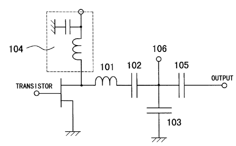
The matching circuit of the first embodiment indicates
a matching circuit according to the present invention as an
output matching circuit. Fig. 1 is an equivalent circuit diagram
of the first embodiment of the present invention, which is made
up of a series inductor 101, a series capacitor 102, a parallel
capacitor 103, a drain bias circuit 104, and a DC blocking
capacitor 105. With the exception of the fact that this circuit
configuration uses a capacitor having a capacitance that is
dependent upon the bias voltage as the parallel capacitor 103,
itisnotmuch different fromamatchingcircuitthatis generally
used.
A thin-film capacitor made of a material such as
(BaXSrl-x)Tio3~ Pb(zrxTil-x)o3~ SrBi2Ti2xNbxO9, BaTiO3, PbTiO3, or
SrTiO3 can be used as a capacitor having a capacitance that is
dependent upon the bias voltage. Of these capacitor materials,
the bias voltage dependency of the capacitance of a (BaxSrlx)TiO3
thin-film capacitor has been indicated, for example, at the 59th
Spring Applied Physics Society, noted in report 28p-ZF-9.
Fig.2showsthebiasvoltagedependencyofthecapacitance
of a (BaxSrlx)Tio3 thin-film capacitor with and without the
application of RF power to the substrate during the film
CA 02239343 1998-06-02
deposition. Because (BaxSrlx)TiO3is polarized by an electrical
field, the capacitance is the largest with a bias voltage of
0 volts. The capacitance decreases as the bias voltage is
increased. In the case in which RF power is applied, there is
a change of approximately 50% in the capacitance as shown in
Fig.2. Therefore, by using a (BaxSrlx)TiO3 capacitor, it is
possible to change the matching conditions with an increase in
output power, that is, with an increase in the voltage applied
to the matching circuit capacitor. And Fig.2 also shows leakage
current of a (BaxSrlx)TiO3thin-film capacitor.
Fig. 3 is a schematic representation of the principle of
the present invention which is shown on the impedance chart.
If the matching conditions that attain good transistor output
and distortion characteristics are both evaluated, the design
can be made so that, with an increase in the output power the
matching condition is changed from a condition that places
emphasis on output power to a condition that places emphasis
on distortion compensation.
Fig. 4 shows the dependency of output power and distortion
output on the input power. A matching circuit according to the
present invention enables attainment of low distortion even at
high output power, without reducing the gain. In a case in which
the direction or absolute value of capacitance change is not
appropriate, it is possible to provide a capacitor bias circuit
connected to a the terminal 106, or to increase the inductance
and capacitance in the matching circuit.
The matching circuit of the second embodiment indicates
a matching circuit according to the present invention as an
output matching circuit. Fig. 5 is an equivalent circuit diagram
CA 02239343 1998-06-02
of the second embodiment of the present invention, which is made
up of a series inductor 501, a parallel capacitor 502 for the
purpose of suppressing the second harmonic frequency, a series
inductor 503, a series capacitor 504, a parallel capacitor 505,
a drain bias circuit 506, and a DC blocking capacitor 507. This
circuit configuration uses a capacitorhaving a capacitancethat
is not dependent upon the bias voltage as the parallel capacitor
502 which is used for suppressing of the second harmonic
frequency, and uses a capacitor having a capacitance that is
dependent upon the bias voltage as the parallel capacitor 505.
With the exception of the fact that this circuit configuration
uses a capacitor having a capacitance that is dependent upon
the bias voltage as the parallel capacitor 505, it is not much
different from a matching circuit that is generally used.
A thin-film capacitor made of a material such as
(BaXSrl-x)TiO3~ Ph(ZrXTi1-X)O3, SrBi2Ti2xNbxO9, BaTiO3, PbTiO3, or
SrTiO3 can be used as a capacitor having a capacitance that is
dependent upon the bias voltage. Of these capacitor materials,
the bias voltage dependency of the capacitance of a (BaxSrlx)TiO3
thin-film capacitor has been indicated, for example, at the 59th
Spring Applied Physics Society, noted in report 28p-ZF-9, in
which it was indicated that, in the case of applying RF power
to the substrate during the film deposition, there is a change
in the capacitance of approximately 50%. Therefore, by using
a (BaxSrlx)TiO3capacitor in a matching circuit, it is possible
to change the matching conditions with an increase in output
power, that is, with an increase in the voltage applied to the
matching circuit capacitor.
Fig. 6 is a schematic representation of the principle of
CA 02239343 1998-06-02
the present invention which is shown on the impedance chart.
If the matching conditions that attain good transistor output
power and distortion characteristics are both evaluated, the
design can be made so that, with an increase in the output power
the matching condition is changed from a condition that places
emphasis on output power to a condition that places emphasis
on distortion compensation. By doing this, it is possible to
attain low distortion even at a high output power. In a case
in which the direction or absolute value of capacitance change
is not appropriate, it is possible to provide a capacitor bias
circuit connected to a the terminal 508, or to increase the
inductance and capacitance in the matching circuit An SiNX
capacitor can be used as the capacitor having a capacitance that
is not dependent on the bias voltage, which is used for
suppressing of the second harmonic frequency. The series
inductor 501 and the parallel capacitor 502 are designed to
achieve a condition in which the second harmonic frequency is
shorted. Because the capacitor used as the parallel capacitor
502 hasacapacitancethatisnotdependentuponthebiasvoltage,
the matching conditions for the second harmonic frequency do
not change with an increase in the output power. Thus, the second
harmonic frequency is always suppressed, enabling the
attainment of a high operating efficiency.
The first effect ofthepresent invention is that, byusing
a capacitor having a capacitance that is dependent upon the bias
voltage, so that as the output power increases the matching
condition is changed from one that emphasis output power to one
that emphasized low distortion, thereby eliminating the
distortion compensation circuit used in the past, it is possible
CA 02239343 1998-06-02
to attain a significant reduction in the surface area occupied
by the circuit. Additionally, the simplicity of the circuit
configuration is effective in reducing cost.
The second effect of the present invention is that, by
using a first capacitor having a capacitance that is dependent
upon the bias voltage so that the matching condition is changed
from a condition with emphasis on output power to one with
emphasis on low distortion, and by using a second capacitor with
a capacitance that is not dependent upon the bias voltage to
achieveshortingofthesecondharmonicfrequency, itispossible
to achieve not only low-distortion characteristics, but also
highly efficient operation, using a simple, compact circuit
configuration. Additionally, by suppressing second and higher
harmonics as well, it is possible to achieve even higher
efficiency.