Note: Descriptions are shown in the official language in which they were submitted.
CA 02239513 1998-06-03
W O 97/21284 PCT~US96/17739
EF~[CIENT APPARATUS FOR SIl\~ULTAN~OUS MODULATION
AND DIGITAL BEAMFORMING FOR AN ANTI~NNA ARRA~
Field of the Disclosure
The present invention relates to digital beamforming, and more particularly to
S an efflcient apparatus for simultaneous modulation and digital beamforming for an
~ntPnn~ array.
Background of the Disclosure
~lectronically steered directive antenna arrays according to the known art use atechnique known as digital beamforming. In digital beamforming, a plurality of
signal waveforms N, which are to be tr~n~mitt~, are l~lcse-lted by sequences of
numerical samples, with the aid of Analog-to-Digital (AtoD) convertors, if necessary.
In general the complex number sequences are applied to the inputs of a numericalprocessor known as a digital beamforming network. The digital beamforming
network computes a number M of numerical output sequences corresponding to the
number of elements in an antenna array that have to be driven. The general complex
output sequences are converted to analog waveforms with the aid of Digital-to-Analog
(DtoA) convertors for mo~ ting a radio frequency carrier using, for example, a
quadrature modulator of a known type. The modulated radio frequency waves are
then amplified for tr~n~mi~ion by respective ~ntenn~ elements. This prior art digital
beamforming network effectively performs a multiplication of a complex vector of N
inputs with an MxN complex matrix of coefficients to form a complex vector of M
outputs, for each time sample of the input signals.
A prior art digital beamforming network is illustrated in Figure 1. Information
signals, which may be analog signals such as speech, are converted to digital signals
~ 25 using AtoD convertors 10. The output signals from the AtoD converter 10 may, for
example, be PCM signals of 8 kilosamples per second of 16-bit cli~iti~fl samples.
The total bit rate of 128Kilobits/sec is usually considered excessive for tr~n~mi.~ion
of digital speech over radio links. As a result, an encoder 11, which may be a
Residll~lly Excited Linear Predictive encoder (RELP) or one of the other known
CA 02239~13 1998-06-03
W O 97/21284 PCT~US96/17739
forms such as Sub-band, CELP or VSELP is used to achieve significant compressionof voice bit rates down to 8 kilobits per second or even lower while preserving
reasonable telephone quality. Such encoders remove as much of the natural
redundancy from speech as possible making received quality more sensitive to bitS errors. It is therefore common to expand the bitrate again by replacing some
rednn(l~ncy in the form of more intelligent error correction coding. The net data
stream is then impressed on a radio wave for tr~n~mi.~ion using any of the knowndigital modulation techniques such as PSK, QPSK, Offset-QPSK, Pi/4-DQPSK,
l~QAM and so on. In PSK, the radio carrier is simply invert'ed in phase depending
10 on whether the data bit being tr~n~mitted is a binary ' 1 ' or a '0' . The abrupt
inversion of the phase gives rise to spectral spreading of the radio signal and potential
interference with other radio channels. Thus, the prior art modulation comprisesfil~Tinp of the digital waveform to round-off the transitions between ' 1' (+ 1) and '0'
(-1). In extreme cases known as partial response .cipn~lling~ over-flltering is used to
15 reduce the amount of spectrum used by a signal for its tr~n~mi~ion. Filtering is used
to obtain desired characteristics in the spectral domain, but can be achieved either
with spectral domain filters such as may be constructed with resistors, inductors and
c~r~ritcrs or may be achieved by processing in the time domain using time samples.
An archetypical time-domain filter is known as the transversal filter or Finite Impulse
20 Response (FIR) filter. Other prior art time domain filters are known as Infinite
Impulse Response filters (II~).
An FIR filter comprises one or more delay stages for delaying the signal to be
filtered forming a tapped delay line. When signals are already in the form of
sequential n--meric~l waveform values, such a tapped delay line may be formed by25 storing samples se(luentially in a digital memory device. Samples delayed by different
amounts are then weighted and added to form the filtering characteristic. Such afilter, when employed to filter digital waveforms, generally produces several output
values per input data bit so as to correctly ,t;~ sent the shape of the 1-0 transitions
which are important in controlling the spectrum to the desired shape. These values
30 are no longer +1 or -1, but any value in between. Thus, premodulation filtering has
the effect of ch~np-ing single-bit information values to a plurality of multi-digit values.
CA 02239~13 1998-06-03
W O 97/21284 PCTnUS96/17739
In prior art beamforming methods, the filtered, multi-valued modulation
waveform is applied to a digital beamformer 13. The digital beamformer forms M
di~re~ tly complex-weighted combinations of the modulation waveforms, which whenmodulated on to an a~p~u~liate radio frequency carrier and applied to corresponding
~ntenn~ array elements, will result in each modulated signal being radiated in aseparate, desired direction. The in-general complex numerical outputs of the
beamformer are DtoA converted using, for example, a DtoA convertor for the real
component followed by a smoothing or anti-~ in~ filter to produce a continuous
waveform between samples, and a similar device for the im~gin~ry part. The DtoA
converted waveforms are known as I,Q waveforms, and are applied to an I,Q
mo~ulator ~or quadrature modulator) which impresses the complex modulation on a
desired radio carrier frequency. The DtoA conversions anti~ cin~ filtering and I,Q
modulator are represented by blocks 14 of Figure 1.
The prior art beamformer thus forms M combinations of the N input signals
samples by means of an MxN matrix multiplication with a matrix of combining
coeffici~ont~. For example, suppose N=320 and N=640; then for each input signal
sample period, 204800 complex multiply-accumulate operations have to be per~ormed.
A typical coded digital speech signal may be represented by a modulation waveform
of lOKHz bandwidth, which, if sampled at 8 samples per cycle of bandwidth in order
to accurately represent 1-0 transitions, leads to 80'K complex samples per second from
each modulation waveform generator 12. Thus the number of complex operations persecond that digital beamformer 13 must execute is 80000 x 204800 =
16,384,000,000.
Instruction execution speeds of digital signal processing devices are measured
in Mega-Instructions Per Second or MIPS. Thus, 16384 MIPS of processing are
required. A complex multiply-accumulate consists however of 4 real multiply-
accum~ t.os in which DSP power is normally measured. Thus, the number of real
MIPS required is thus 65536, or with allowance for overhead, > 100,000.
A state of the art digital signal processor such as the Texas Instruments
TMS320C56 executes about 40MIPS. Thus, 2500 devices are needed for the
post~ t~ 320-input, 640-output beamformer. This may also be expressed as 8 DSP's
CA 02239~13 1998-06-03
W O 97/~1284 PCT~US96/17739
per voice channel. As state of the art DSPs are expensive, the use of 8 DSPs pervoice ch~nnel raises the cost of providing communications infrastructure which is
measured in terms of cost per in.ct~lled voice channel.
Summary of the Disclosure
It is therefore an objective of the invention to provide digital beamforming andspcctrally controlled modulated output signals at a reduced cost per voice channel,
which may be achieved by practicing the invention according to the following
description and drawings. The present invention relates to a beamforming networkwhich is adapted for tr~n~mitting ~ digital information streams using M antenna
elements. The N digital information streams are represented by binary l's and O's, or
in ~rithm~tic units, by + 1 or -1. These unfiltered digits form the inputs to the
inventive beamformer, which no longer have to perform multiplication. Furthermore,
precomputed sums and differences may be stored in look-up tables addressed by
groups of bits of the information streams, in order to save computational effort.
Since the beamforming network performs a linear operation, filtering of the digital
information waveforms in order to delimit the transmitted spectrum can be performed
on the output signals rather than the input signals, thus permitting the simplification of
the beamforming process.
According to one embodiment of the present invention, a digital beamforming
network for transmitting a first number of digital information signal using a second
number of antenna array elements is disclosed. Assembling means are used for
assembling one information bit selected from each of the information signals into a bit
vector. Digital processing means have an input for the bit vector and a number of
outputs equal to the second number of ~nt~.nn~ elements and process the bit vector.
Finally, modulation waveform generation means coupled to each of the second
number of outputs generate a signal for tr~nsmic~ion by each ~ntenn~ element.
According to another embodiment of the present invention, a digital
beamformer for tran~mitting a first number of digital information streams using a
second number of ~ntenn~ array elements is disclosed. The beamformer has selection
means for sele~ting one information bit at a time from each of the information streams
CA 02239513 1998-06-03
W O 97/21284 PCT~JS96/17739
and assembles them to form a real bit vector and selects another information bit from
the information streams to form an im~gin~ry bit vector in a repetitive sequence.
Digital processing means repetit*ely process the real bit vectors ~ltern~tely with the
im~gin~ry bit vectors to obtain for each of the second number of ~ntenn~ elem~nt~ a
5 first real and a first im~in~ry digital output word related to each real bit vector and
obtains a corresponding number of second real and second im~gin~ry output words
related to each im~gin~ry bit vector. Switching means selects the first real digital
output words alternating with the second im~gin~ry output words to produce a stream
of real OQPSK modulation values and alternately selecting the second real digital
10 output words alternating with first im~gin~ry output words to produce a stream of
im~in~ry OQPSK modulation values. Modulation waveform generation means
process for each of the ~ntenn~ elements the real and im~in~ry OQPSK modulation
values to obtain a corresponding OQPSK modulated radio waveform.
13rief Desçription of the Drawings
These and other features and advantages of the present invention will be more
readily understood upon reading the following det~ile~ description in conjunction with
the drawings, in which:
Figure 1 illustrates a prior art multiple beamforming network;
Figure 2 illustrates a beamforming network according to one embodiment of
20 the present invention;
Figure 3 illustrates generating filtered PSK according to a known method;
Figure 4 illustrates a mlm~ric~l generation of filtered modulated waveforms;
Figure 5 illll~tr~ted an implementation of the waveform generator illustrated inFigure 2;
~5 Figure 6 illustrates beamforming using precomputed look-up tables;
Figure 7 illustrates the use of 16 megabit DRAMs for beamforming according
to one embodiment of the present invention;
Figure 8 illustrates a DRAM for forming staggered interstitial beams between
different channels;
CA 02239~13 1998-06-03
W O 97/21284 PCTnUS96/17739
Figure 9 illustrates time~h~rin~ the inventive beamformer between different
fre~uency chAnn~s;
Figure 10 illustrates a beamformer used in con3unction with digital frequency
division multiplexing;
Figure 11 illustrates the generation of offset QPSK modulation waveforms;
Figure 12 illustrates an arrangement for offset QPSK beamforming according
to one embodiment of the present invention;
Figure 13 illustrates the use of the inventive beamformer for reception with
har-llimitin~ channels; and
Figure 14 illustrates the use of the inventive beamformer for receive
procee~ing of multi-bit quantities.
I)etAiled Description
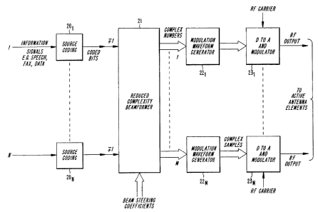
The inventive beamformer is illustrated in Figure 2. The Analog to Digital
conversion (Fig. 1 (10)), voice coding and error correction coding ~Fig. 1 (l l)) have
been abbreviated to the source coding block 20 of Figure 2. Source coding comprises
reducing analog voice, pictures, documents for faxing or any other form of
information to a digital bitstream for trAncmic~ion, and may comprise AtoD
conversion, data compression to remove redundancy and error correction and/or
detection coding to improve trAn~micsion reliability.
The output of the source coding may be represented arithmetically as a
sequence of +1 or -1's at the rate of one such number per information bit. This is a
much simpler sequence than is produced by the modulation waveform generator 12 of
Figure 1. Typically, the latter produces 8 multi-bit complex numbers per data bit,
because it filters the digital data waveform for trAn~mi.scion to constrain the spectral
occupancy. The present invention relies on the principle that the beamforming
network Lle ~ ns a linear operation, and that the modulation waveform generation is
a linear operation, and thus their order can be reversed. According to the present
invention, modulation waveform generation is performed after beamforming, thus
avoiding an expansion from one single bit value per information bit to several multi-
bit values ahead of the beamformer. Thus, the beamformer has to perform operations
CA 02239~13 1998-06-03
W O 97/21284 PCT~US96/17739
at typically 1/8th of the rate. Instead of multpilication, the beamformer only has to
perform N additions or subtractions (according as an input bit is + 1 or -1) of an
associated predetermined beamforming coefficiçnt For example, if the beamformingcoefficient.c for signal i's desired transmit direction are cli,c2i,c3i...cmi, and the bits
for signals i=1,2,3,4.. n are +1,-1,+1,+1.... +1, then the beamforming network
must calculate:
~QUATIQN SET 1
cl l-c12+c13 +c14.. +cln for array element 1
c21-c22+c23~c24.... +c2n for array lement 2 and so on.
The +/- sign pattern in forming the combinations corresponds to the data bit
polarities at the input. If each cik is in general a complex number, the above
r~esen~ 2nm additions or subtractions compared to the 4nm multiply-accumulates of
Figure 1. Moreover these need only be performed at typically 1/8th the rate, a total
saving factor of 16. This translates into a cost per voice channel reduced from 8
15 DSPs to 0.5 DSPS, which is affordable.
Before continuing to explain how even greater saving may be achieved by the
use of precomputed look-up tables, the function of the modulation waveform generator
22 which is now p~aced after the beamformer will be explained. When linear
modulation is used, data bit waveforms are filtered to contain spectral occupancy and
20 then modulated on to a radio frequency carrier using for example AM, PSK, QPSK,
DQPSK, OQPSK, etc. Linear modulations give rise to a varying radio frequency
amplitude as well as a varying phase, whereas non-linear modulations such as FM,PM, FSK, MSK, GMSK, CPFSK and the like are used when it is desired to m~int~in
a constant amplitude signal that is modulated only in phase. The latter may be
25 preferable for tT~n~mitting a single information stream, such as in a digital mobile
phone, because constant envelope tr~n~mittPrs can operate at greater efficiency. In an
active phase array tr~n~mittin~; a multiplicity of signals, the composite signals
- tr~n~mitt~d by each element are inevitably of varying amplitude and phase, and it is
thus no disadvantage, to use the more spectrally efficient linear modulation methods
30 which require varying the amplitude.
CA 02239~13 1998-06-03
W O 97/21284 PCT~US96/17739
--8--
The simplest linear modulation method for digital information is PSK. PSK is
effectively Double Sideband Su~ressed Carrier amplitude modulation (DSBSC) of the
radio carrier wave with the filtered bitstream. Figure 3a shows the waveforms used
for generating filtered PSK with a known balanced modulator 30a. An unfiltered data
5 waveform 32a is applied to a bandwidth-restricting, low-pass filter 31a producing
filtered waveform 33a. The filtered waveform multiplies the radio frequency carrier
34 in balanced modulator 30a to produce modulated waveform 35a. In the modulatedwaveform, the RP carrier wave has been inverted 180 degrees in phase for periodswhen the filtered waveform is negative, corresponding to binary 'O's in the origina~
10 data stream. A currently more fashionable approach to modulation is shown in Figure
3b. The data bit waveform is regarded as a series of impulses 32b of ~ or - signinstead of a flat-topped square wave 32a. These impulses are applied to shock-excite
a filter 31b that rings in response to each impulse in a characteristic way known as the
impulse response. Since the ~llter is linear, the output waveform 33b is the linear
15 superposition (addition or subtraction according to the sign of the data bit) of the
impulse responses produced by each data impulse. This waveform then modulates RFcarrier 34 as before using b~l~nce~ modulator 30b to produce modulated radio wave
35b. Waveforms 33b and 33a are similar, as are waveforms 35a and 35b. ~he
systems of Figures 3a and 3b are in fact identical when the filter frequency responses
2û H~jw) and H'(jw) are related by:
~I'(jw) = H(jw).SIN(wT) where T is the data bit period.
wT
Modern theory contends that impulse responses H'(jw) that are not constrained
to contain a Sin(wT)/wT factor can be made more desirable. The advantages are a
~5 better spectral containment without reducing communications efficiency through
overfiltering, and better demodulation algorithms are possible through being better
able m~thp~m~tically to model the tr~ncmiccion process as the impulse response of a
transmit filter, propagation chzlnnçl and receive filter combined. Furthermore, if this
combined ch~nnel has the Nyquist property, which means that its combined impulse30 response has ~ero-crossings at multiples of the data bit period away from the peak,
then the received signal, when sampled at the correct instants, will reproduce the dat~
CA 02239~13 1998-06-03
W O 97/21284 PCT~US96/17739
bit polarities without corruption due to smP~rin~ of neighboring values, i.e., without
Intersymbol InlelrerGIlce (ISI). A common design technique is to ensure that, at least
for an ideal propagation channel, the combined impulse response of the transmit and
receive filters is Nyquist. An arbitrarily equal allocation of the overall Nyquist
S response is then made to the transmit and receive filters respectively, so each are
lm~ to have the square root of the Nyquist filter's frequency response. The
tr~n~mitt~r filter may be made root Nyquist, but there is in practice less control over
the receiver IF filters. Nevertheless, the deviation from root-Nyquist at the receiver
is simply modelled as a linear imperfection introduced by the propagation channel and
can be compensated by an equalizer of known type.
~dvantageous means exist for numerically generating modulation waveforms of
data impulses filtered by a root-Nyquist filter or indeed any filter. The design process
is as follows. Once the desired Nyquist filter response is chosen, the square root of
its frequency response is calculated. Then, the impulse response of the root-Nyquist
filter may be calculated by Fourier transforming its frequency response. The impulse
response is in general a continuous waveform, but it can be represented adequately by
a number of sample values greater than twice the maximum frequency at which its
frequency response is non-zero and still significant. In practice, the sample rate used
is expressed as a multiple of the data bitrate and is chosen to make the smoothing
filter needed to smooth the samples waveform as simple as possible. It is desirable
that this filter, which must be a continuous time filter constructed with analogcomponents, be of broader bandwidth than the desired root-Nyquist response so that
tolerances in its cut-off frequency do not affect the overall response, which should be
domin~ted by the accurate digitally generated root-Nyquist characteristic.
The scheme for mlmeric~lly generating filtered modulation waveforms is
str~tP~l in Figure 4. Data bits are clocked into shift register cells 40...45 and bits
delayed by 1,2,3,4,5 or 6 bit periods are made available from taps on the shift
register to digital calculator 46. For each shift, the digital calculator computes:
EQUATION SET 2
S0 = bl-F(-3T) + b2-F(-2T) + b3-F(-T) + b4 F(0) + b5-F(T) + b6-F(2T)
Sl = bl-F(-2.9T) + b2 F(-1.9T) + b3 F(-0.9T) + b4-F(0.lT). . .b6-F(2.1T)
CA 02239~13 1998-06-03
W O 97/21284 PCT~US96/17739
-10-
S2 = bl-F(-2.8T) + b2-F(-1.8T) + b3-F~-0.8T) + b4-F(0.2T). . .b6-F(2.2T)
.
S8 = bl-F(-2.2T) + b2-F(-1.2T) + b3-F(-0.2T) + b4-F(0.8T). . .b6-F(2.8T)
S S9 = bl-F(-2.1T) + b2 ~(-l.lT) + b3-F(-0.lT) + b4-F(0.9T). . .b6-F(2.9T)
where F(t) is the impulse response of the desired filter at a time 't' away from the
peak, T is the bit period, and the above assumes that 10 waveform samples per bit
period are to be computed (i.e. Nl of Figure 4 is equal to 10). If 8 samples per bit
had been desired, then the arguments of F(t) would have been incremented in steps of
10 T/8 instead of O. lT.
Since the impulse response F and the times at which its value is needed to
calculate the above are known in advance, all the 60 F values in the above formulas
may be precomputed and stored in a look-up table or read-only memory. Even better,
because the data bits bl...b6 can only jointly take on 64 different combinations, each
15 value SO....S9 can only take on one of 64 possible combinations of the F values, the
combinations of which can then be precomputed and stored in a table of 64 values for
SO, 64 values for Sl... and so on, a total of 640 values. This is a relatively small
~ead Only Memory (ROM) by today's standards, so it is possible to obviate
calculation altogether by substituting a ROM table for digital calculator 46 which is
20 addressed by shift register 40...45.
The output from the digital calculator 46 is thus a stream of Nl values per databit. This may be applied to a DtoA convertor 47 to generate a corresponding
sequence of analog c~mI~lec 48. This waveform has discontinlliti~s between samples
that must be smoothed out to avoid spectral spreading of the tr~ncmiccion. The
25 discontinuities occur however at the relatively high frequency of the sample rate
which is N1 times the bitrate. Therefore, they may be filtered out by a continuous
time filter 49 with a frequency response that cuts off at several times the bitrate, and
thus does not affect the frequency response in the region around the bitrate that we
are attempting to accurately define. Any small residual effect that filter 49 may have
30 on the overall root-Ny~luist response can be taken into account in precomputing the F-
coefficients defined above. The F-coefficients can for example be computed from the
CA 02239~l3 l998-06-03
W O 97/21284 PCT~US96/17739
impulse response of the desired root-Nyquist filter times an approximate inverse of the
lter 49.
An advantageous alternative technique shown by blocks (51...54) is disclosed
in U.S. Patent Application 07/967,027 and U.S. Patent Application 08/305,702,
5 which are both hereby incorporated by reference.
The Nl samples per bit produced by the digital calculator 46 is subjected to a
first stage of mutation towards a continuous waveform by filling in extra samples
between the original samples using a digital interpolator 51. This may for example be
a simple linear interpolator that simply draws a straight line between original samples
10 in order to çstim~te the value of intervening samples. Samples at the interpolated rate
are then applied to a high bitrate Sigma-Delta convertor 52, which represents the
waveform as the proportion of l's to 0's in a much higher bitrate stream. The
inverse of this bit stream is also formed by an invertor 54 and the stream and its
inverse are applied to a balanced (push-pull) continuous-time filter arrangement 53 to
15 generate the desired continuous waveform. One advantage of alternative arrangement
(~1..54) is the elimin~tion of the DtoA convertor 47, and other advantages are
~liccu~eA in the aforementioned applications incorporated above.
A modified arrangement similar to Figure 4 can be employed to implement
modulation. The mo-lif1c~tion is required because the input quantities to the post-
20 beamforming modulator have been transformed into multi-bit complex values by the
combinatorial beamforming operation and are no longer single bit values as in
Figure 4.
Figure 5 illustrates the modified waveform generator. A sample stream
comprising the real parts of the complex number stream from one output of
beamformer 21 is delayed in a series of memories (60.. 61,62) corresponding to the
length of the impulse }esponse of the transmit filtering desired. A convolver 63 forms
Nl output samples per input sample shifted into delay elements 60...62 by computing
e~luation set 2 substit-ltin~ for bl...b6 the multi-bit input values from the delay
element~. This now involves full multiplications as bl...b6 are no longer just +/-l.
30 However, the number of multiplications needed to implement the filtering operation is
much less than the number needed to implement beamforming. Therefore, it is
CA 02239~13 1998-06-03
W O 97/21284 PCT~US96/17739
-12-
advantageous to simplify beamforming at the expense of modu}ation filtering
complexity. A convolver 66 is identical to the convolver 63 and deals with the
im~gin~ry part of the complex number stream from an output of the beamformer 21.Those skilled in the art of digital design will recognize the possibility to time share a
5 single convolver between real and im~gin~ry operations for further simplification.
The multiplications performed by the convolvers 63 and 66 are moreover with fixed
constants unlike the multiplications performed by the beamformer 21, ~c~lming the
beams are to be dynamically steered by varying the coefficients. Thus, a simplerpiece of digital hardware can be constructed to perform convolving with fixed
10 constants than matrix multiplication with variable quantities.
The output values from convolvers 63 and 66 comprise a complex number
stream at an elevated sample rate of Nl samples per original data bit period. These
samples are converted to analog waveforms for mod~ ting the radio wave by the
Interpolation and Sigma-Delta technique described above, using convertors 67 and 68
15 and balanced filters 69 and 70. The b~l~nce~ I,Q waveforms are applied to b~l~n~ed
I,Q modulators 71, 72 and 73 along with cosine and sine waveforms at the radio
carrier frequency to obtain a signal for tr~n~mi~ion by a phased array element (not
shown).
Further simplifications of the beamforming network 21 that are possible when
20 input values are only + 1 or -1 (binary 1 's and O's) will now be explained. The
equation set 1 describes the computations to be performed. It is in fact identical to
the equation set 2 when, instead of the determined signs, multiplication by +1-1according to the data bit polarity is shown as in the equation set 2. Thus, the
expression for array element l's unfiltered signal becomes:
El = bl cl 1 +b2-c12+b3 c13+b4-c14.. +bn-cln for array element 1
A subset of these terms, involving, ~or example, the eight bits bl...b8, can
only take on, in that example, 256 possible values as the 8 bits can have only 256
different combinations and the coef~lcients are fixed at least for a l~rge number of
sample computations. Thus all 256 possible values of
bl c11+b2 c12+b3 c13+b4 c14+bS c15+b6 c16+b7 c17+b8 c18
CA 02239~13 1998-06-03
W O 97/21284 PCT~US96/17739
may be precomputed and stored in the table T(bl,b2,b3...b8), from which they can be
retrieved by addressing the table with the 8-bit address bl,b2,b3...b8. Since 65536-
word semiconductor memories are single, low-cost components in today's technology,
even the combination of 16 bits can be precomputed and stored. A very efficient
S means of precon,puling such tables is to explore all 16-bit patterns by ~h~nging only
one bit at a time, in so-called Grey-code counting order. Then each sllcces~ive value
computed is equal to the previous value plus or minus twice the value of the c-
coefficient associated with the changed bit, an effort of only one addlsubtract per
computed value.
A similar table may be computed for bits 17.. 32; 33.. 48 and so-on.
Finally, with such tables, El is computed from:
El = Tl(bl...bl6) + T2(b17....b32) + T3(b33....48) .......
The number of additions required has thus been reduced in this way by a
factor of 16. The addition of the outputs of the tables may be performed by
15 combining them in pairs using a binary tree structure and serial arithmetic adders, as
shown in Figure 6.
A group of 16 data bits bl...bl6 is applied as an address to a precomputed
RAM table 80. An 8-bit real and an 8-bit im~gin~ry value are obtained. A similarprecomputed partial sum is obtained from a RAM table 81. The real and im~gin~ry
values are serialized by parallel-serial convertors 83, 84, 85, and 86 for application of
thevalues bit serially to serial arithmetic adders 87 and 88. The sum Rl+R2, Il+I2
appears as a serial digital value from adders 87,88 and is combined in turn with a
further sum in a tapering adder tree until the final stage 89 and 90 completes the
calculation of El. The advantage of serial arithmetic for addition of multiple values
is simple implementation using integrated circuit technology, and no throughput delay,
as disclosed for calculating Fast Walsh Transforms in U.S. Patent Application No.
07/735,805 which is hereby incorporated by reference.
R~c~lling that the data rate per channel originally mentioned for coded speech
was in the neighborhood of lOKB/S, the network illustrated in Figure 6 only needs to
calculate an output value every lOOuS. This is an extremely slow speed for accessing
memory tables, which are capable of much higher speeds, for example 10 megawords
CA 02239~13 1998-06-03
W O 97/21Z84 PCTAJS96/17739
per second. One method of capitalising on the excess speed available is to use Figure
6 for a TDMA system in which perhaps 1024 speech bit streams are time-multiplexed
into 10MB/S bitstreams. Thus, the number of signals the network handles is 1024N.
If the coefficient tables are the same for ever,v timeslot, it means that the N TDMA
signals are radiated in the same set of directions for all timeslots. Other structures
will be disclosed that can vary the directions on a timeslot-by-timeslot basis.
For example, a 256-beam system using 512 phased array elements can be
constructed according to Figure 6 using sixteen, 65kword memories for forming each
array element signal, a total of 16x512 = 8192 memory chips-. Note however that this
can handle 256 signals in each of 1024 timeslots of a TDMA frame, thus the capacity
is 262,144 voice channels and the complexity per voice channel is 8192/262144 =
1/32nd of a RAM chip per voice channel. This indicates the economic possibility to
construct very large phased array communications systems for very high capacity
communications systems.
A dirre,~ t way of ~Itili7ing the excess memory speed available in Figure 6 is
shown in Figure 7. Dynamic RAM chip sizes become ever larger driven by
commercial competition in the computer market. The 16 megabit DRAM is now on
the verge of commercial production. It is assumed in Figure 7 that 16 megabit
DRAMs will be available organized as 220 16-bit words, having thus 20 address pins
and 16 data pins. A DRAM 100 is used to hold precomputed combinations of signalsbl...bl6 for 16 array elements. The precomputed values are stored as serial values
occupying one bit, for example the least signifi~zlnt bit, of 8 consecutive words to
represent an 8-bit real part and the next eight consecutive words for an 8-bit
im~gin~ry part. Another bit of those same words (for example the 2nd least
25 ~i~nific~nt bit) stores similar information for array element 2, and so-on. Each 16-bit
word thus contains one bit of a real or im~gin~ry value for 16 array elements. A bit
of an 8-bit real value is addressed by the three "bit-address" lines while the real or
im~oinz~ry part is selected by the R/I address line. By using these address lines, the 8
bit real value can be serially output followed by the 8-bit im~gin~ry value. Serial
30 values are obtained in this way without the use of the parallel to serial convertors 83
to 86 of Figure 6, and for 16 array elements ~imult~neously. The DRAMs 100,101
CA 02239513 1998-06-03
W O 97/21284 PCT~US96/17739
are addressed thus 16 times faster than in Figure 6, namely at 16 times the coded
speech bitrate, or around 160kilowords/sec. This is still well within the speed of
DRAMs.
A corresponding pair of s~qri~li7ed partial sums is now extracted from pairs of
S DRAMs, for example 100 and 101, and combined in a serial adder 102. The serial
output of the adder 102 is further combined with a similar output in an adder 103 and
so-on through the binary tree to the final output from an adder 104.
When all 8 bits of the real values have been added, the inputs to the adding
tree 102,103...104 are frozen at the last bit polarities, which are the signs of the
values, and clocks continue to be applied to the adder tree to clock through carry
propagation, which forms the most signific~nt bits of the sum output. During this
time, the im~in~ry values are clocked out of the DRAMs 100,101 and are added in a
second adding tree (not shown) for the im~in~ry parts.
A system of 256 signal inputs and 512 array elements constructed according to
Figure 7 uses 16 DRAM chips plus a serial adder tree to form signals for 16 array
elements, thus 32 such structures are required for all 512 elements, a total of 512
DRAM chips. This represents a complexity of 2 I~RAM chips per voice channel, butthey are not at all used at full speed. The addressing speed may be increased by a
factor of 64 from 160 kilohertz to 10 megahertz, thus allowing re-use of the structure
for 64 timeslots, giving a capacity of 64 x 256 voice ch~nn~l~ and a comp}exity of
1/32nd of a DRAM per voice channel, as before. The RAM chips are however much
bigger, i.e., 16 megabit chips compared with the 1 megabit chips of Figure 6. This
pe~ s the elimin~tion of the parallel-serial convertors of Figure 6, but this may or
may not be an economic trade-off. Many factors influence this trade-off such as the
number and total area of printed circuit board for mounting 8192 chips as in Figure 6
with the equivalent p~çk~jng cost of 512 chips for figure 7. The trade-off also
depends on whether a wideband, 1024-timeslot TDMA system is desired, or a
narrower band TDMA system with fewer slots is desired. It is of course also possible
by one skilled in the art of digital design to adapt the present invention to time share
the beamforming hardware for forming beams on different carrier frequencies instead
of different timeslots, thus taking advantage of the excess speed available with Figure
CA 02239~13 1998-06-03
W O 97/21284 PCT~US96/17739
6 over that needed to handle a single set of 10kilobit voice signals. In that case, the
set of beam directions formed are the same at all carrier frequencies using Figure 6
hardware, as they were on all timeslots of a TDMA system. It can however be moredesirable to form sets of beams that point in difre~nt directions for dirrelt;nt timeslots
5 or carrier frequencies. The use of such interstitial beams is described in U.S. Patent
Application No. 08/179,953, which is hereby incorporated by reference in its entirety.
Figure 8 shows adaptation of the invention to form different sets of beam directions
for different "channels", where a channel may be a frequency, a timeslot, or a
combination. Only that part of Figure 6 equivalent to RAM 80 is shown adapted in10 Figure 8, as it will be obvious to one skilled in the art how the adaptation may be
carried to completion.
A 1-megaword x 16-bit DRAM 110 contains partial sums for 16 data bits
(16384 combinations) and for 16 different communications channels. The channel is
selected by the rem~ining 4 address lines. The rest of the structure can be as in
15 Pigure 6. In a 16-slot TDMA system, the first bits of all signals for transmission in a
particular timeslot is applied to inputs bl...bl6 and to any other RAMs, while timeslot
0 (binary 0000~ is applied to the other four address bits of every RAM. Successive
data bits are then applied holding the channel select bits at 0000 until the end of the
timeslot. Then the first data bits to be transmitted in the second timelsot are applied
while the channel select bits are changed to 0001, and so on to channel 1111 at which
point the sequence repeats. For a 256-beam, 512-element array, 8192 DRAM chips
are used and tim~sh~red by 16 timeslots. The complexity has thus increased to 2
DRAM chips per voice channel for the privilege of varying the beam directions from
timeslot to timeslot. The available speed is however still under-utilized when only 16
timeslots are employed. If the number of timeslots is increased to better utilize the
RAM speed capability, either it is necessary also to increase the RAM size above 16
megabits or to accept that some timeslots must use the same set of beam directions, as
only 16 different sets of beam directions are available. This is however sufficient to
achieve the obiectives of U.S. Patent Application No. 08/179,953 of only using each
beam for communicating with stations located out to 25 % of the beam -4dB radiusfrom beam center.
CA 02239~13 1998-06-03
WO 97nl284 PCT/US96/17739
Figure 9 illustrates how the inventive beamforming arrangement can be
fime~h~red between different frequency ch~nnçl~ i.e., for an FDMA system. A
beamformer 120 receives successively signal data bits 121 (bl,b2....bn) for
tr~ncmi.e~ion in a set of beams formed on radio channel frequency 1, determined by
setting the oh~nnçl number address bits to 120 to channel 1. The ~nt~-nn~ element
signals in digital form are output from the beam former into a set of latches for
ch~nnel 1 and control unit 127 toggles a strobe signal to cause the latches to register
these values. Figure 9 shows only the latch 125 for element 1 of channel 1. There
are also latches (not shown) for element 2, 3, 4 etc all for channel I signals. The
control unit then sets the channel number to 2 and a second set of bits 122 for
tr~nsmi.c~ion in a second set of beam directions on channel 2 is presented to
beamformer 120. The outputs for channel 2 are latched in a second set of latches for
channel 2, of which only the latch 124 for element 1 is shown. After cycling through
all channel frequencies in this way, the control unit retùrns to calculate the next
samples for channel 1, and so on. This latch 125 becomes set to successive channel 1
values, that then must be subjected to filtering using a modulation waveform generator
125 such as illustrated in Figure 5. The filtered I,Q modul~ting values are then DtoA
converted in converter 128 and modulated on to radio channel frequency 1 using an
I,Q or quadrature modulator 129. A second filtered waveform generator 126 and
DtoA converter 131 and modulator 132 deal with channel 2 signal for element 1. The
outputs of 129,132, etc. for successive channel frequencies are then added to form a
composite signal for tr~n~mi~ 3n from element 1, and similar set s of equipment form
corresponding signals for elements 2...M.
It is desirable in a pure FDMA system with large numbers of channels and
25 ~nt~nn~ elements to reduce the number of modulation waveform generators
(125,126...) which would otherwise be equal to the product of the number of
frequency channels and the number of ~nt~-nn;~ elements. Since in a pure FDMA
system the bandwidth and therefore the bit and sample rate of each channel is much
lower than a digital circuit, such as in Figure 5, can handle, it is also possible to
3~ consider time-sharing the modulation waveform generators between channels. It is at
least possible to time share the convolvers 63 of Figure 5, which form FIR filters, by
CA 02239~13 1998-06-03
W O 97/21Z84 PCT~US96/17739
-18-
providing a separate set of registers (6(~...62) and (64...65) for each channel. The
latch 123 is in fact the first stage (64 and 60) of such complex registers for channel
19 element 1, while latch 126 is the first of a bank of registers for channel 2. Thus by
providing an array of latches/registers for each ch~nnel plus means to select all the
5 latches associated with one channel as inputs to convolvers 63 and 66, it is possible to
share the convolvers between ch~nnel~. Whenever such an array of registers is
required, a person skilled in the art will recognize that a Random Access Memorychip can represent a suitable implementation.
The number of DtoA converters and modulators may also be reduced by
10 digital techniques. It is desirable to avoid a multiplicity of such analog circuits which
are not so suitable for bulk integration on to integrated circuit chips.
The function of the modulators is to convert each channel signal to its own
radio frequency and to add signals on different frequencies in summers 130. ThisFrequency Division Multiplexing may also be performed using high speed digital
15 techniques. The task is to compute a sufficient number o~ samples per second of a
sum such as:
So + Sl exp(jdW t) + S2 exp(j2dW t) + S3 exp(j3dW t) .. +Sn exp(jndW t)
This expression can be alternatively written as:
So + exp(jdW t) [Sl + exp(jdW-t) ~S2 + exp(~dW t) [S3 + exp .. ].. ~
20 where dW is the channel spacing in radians/sec, and n is one less than the number of
frequency ch~nn~ The sequence of frequencies O,dW,2dW...ndW may
alternatively be centralized instead between -ndW/2 and +ndW/2 by forming:
S L-eXP(jLdW-t) + S L+I ~ exp(j(L-l)dW t) .... + S ,-exp(jdW-t) +
S~ + Sl exp(jdW t)
............ + SL exp(~LdW t) where L = n/2 and n is ~sumçcl even.
L
This latter expression can also be written:
CA 02239513 1998-06-03
W O 97/21284 PCT~US96/17739
-19-
O-S[(S-L + SL) cos(LdW t) + (S L~ I + SL ,) cos((L-l)dW t) .. +(S, + S,).cos(dWt)~
+ So +
jO.5 [(SL_ S L) sin(LdW t) ~ (SL.I-SLI ,) sin((L-l)dW t) . . + (S, - S ,)-sin(dWt)]
Thus using the latter expression, by forming a cosine modulation (1-
S modulation) from the sum of a pair of channel signals and a sine modulation (Q-
modulation) from the difference, the number of I/Q modulators may be halved. This
technique, known as Independent Sideband Modulation ~ISB) places one signal on afrequency negatively offset from center and another signal on~the same frequency but
positively offset from center. Such techniques generally result in imperfect isolation
10 between ~h~nn~l~ due to hardware imperfections in modulators, such as carrierimb~l~nce, imperfect quadrature between cosine and sine signals, and so-on. These
techniques perform much better in a multi-element array context however, as the
imperfections are not correlated from one antenna element channel to another, while
the wanted signal components are. The unwanted signals thus tend to be radiated in
1~ random directions and a proportion of such imperfection energy is, in a satellite
system for example, harmlessly radiated into space, missing the earth altogether.
The arguments of the complex exponentials such as LdW-t are computed at
sllccessively increasing values of t, and reduced modulo-2Pi. The increments of 't'
must comprise at least the Nyquist sampling of the carrier frequency LdW involved.
20 This sampling rate can be greater than the sampling rate for the signals Sl,S2, etc
produced by convolvers 63 and 66, and so further upsampling of the channel signals
must take place in the FDM process.
The above expressions may be recognized as a Pourier Transform. There are
many ways to perform Fourier transforms numerically, such as the Discrete Fourier
25 Transform and the Fast Fourier Transform. It is beyond the scope of this disclosure
to describe all methods for digitally performing a frequency division multiplex, and it
suffices to envision a digital FDM unit with a number of numerical input sequences at
a filrst sample rate per channel comprising signals to be Preqùency Division
Multiplexe~, and producing an output numerical sequence at a second, higher sample
30 rate le~les~..ting the multiplexed signal. The first, lower sample rate is that produced
CA 02239~13 1998-06-03
W O 97/21284 PCT~US96/17739
-20-
by per-ch~nnel, modulation waveform generators such as the upsampling convolvers63 and 66 of Figure 5, and the second, higher sampling rate is at least equal to the
Nyquist rate for the highest frequency present in the FDM output.
The numerical FDM output, conci~ting of a stream of complex numbers for
S each array element, is then DtoA converted in I and Q DtoA convertors and applied
to a single quadrature modulator per array çl~mPnt The arrangement showing use of
a digital FDM unit is given in Figure 10. A timing and control unit 127 controls the
succe~ive present~tion of bit vectors (bl ... bn); (b(n+l) .... b2n) and so forth to
timeshared beamformer 120 which can function in accordance with foregoing
principles. ~ach bit in the bit vectors ~ sents one bit from a communications
ch~nnPl, such as a voice channel, which are to be simultaneously tr~n~mittPcl using
different directive beams and frequency ch~nnelc For example, if each of n
frequency channels can be re-used for a different conversation in each of N different
directions, a total of nN voice ch~nnel~ can be communicated simultaneously. Theaforementioned bit vectors are formed by selecting one bit from each of said voice
ch~nnP,l ~
The beamformer com~ines N of the bits from first N channels to be
tr~nsmitt~-d on frequency 1 to obtain M array element output samples. Each sample is
fed to an associated digital FDM unit 140. Only the ~DM unit 140 for the first array
element is shown in Figure 10. The control unit 127 then causes the second bit
vector to be presented to the beamformer 120 and simultaneously connects the channel
number of frequency 2 to the channel address inputs of the beamformer 120. This
causes generation of a set of element signals that will result in the second set of bits
being radiated on a second frequency using a second set of beam directions.
Successive present~tion of bit vectors to the beamformer 120 along with appropriate
channel numbers thus results, for each antenna array element, in a successive stream
of corresponding complex output samples representing signals to be tr~n~mitt~d on
different radio center frequencies. After one complete cycle of computation using all
eh~nnel numbers once, the digital FDM unit will have stored the samples for eachchannel number and will calculate a corresponding FDM output se~uence representing
said samples tr~n~l~ted to respective relative channel frequencies. By relative channe~
CA 02239~13 1998-06-03
W O 97t21284 PCTnUS96/17739
frequency it i5 meant that the absolute channel frequency, which may be in the several
Gigahertz range, has been removed and the numerical sample stream represents thecomposite signal around a center frequency of zero, or a low frequency compatible
with the digital FDM unit's computation speed. The FDM sample stream is then fed5 to a high speed DtoA convertor 141 where the sample stream is converted to I and Q
modulation waveforms and modulated on to the desired radio frequency. It can of
course first be modulated on to a suitable interme~i~t~ frequency which is then
converted to a final fre4uency using an upconvertor. These details are a matter of
design choice and are not funfl~ment~l to the present invention. The modulated, final-
10 frequency signal may then be amplified to a desired transmit power level and fed toan array ~lemPnt The power amplifier for this purpose may be integrated with the
~n~elln~ array element.
The inventive beamformer described herein switches the usual order of the
operations of "modulation waveform generation" and "beamforming" in order to
15 simplify the latter. The simplification arises due to the sample rate and word length
çxp~n~ion that normally take place in a modulation waveform generator. Avoiding
this expansion until after beamforming calculations are performed ~ignific~ntly
reduces beamforming calculation complexity and allows the use of precomputed
memory tables. The advantage of avoiding sample rate expansion before
20 beamforming becomes even more evident when the invention is applied to a CDMAsystem. In a CDMA system, different signals are communicated not by allocating
them dirr~lc;nt frequencies or different timeslots on the same frequency, but byallocating them dirrel~nt spreading sequences. A spreading sequence of a high bitrate
is combined with an information stream of a low bitrate to deliberately spread its
25 spectrum. Several signals using dirrel~nt spreading sequences are transmittedoverlapping in both time and frequency. The receiver despreads a wanted signal
making use of its known spreading code, thus compressing the signal to a narrowband
- signal once more. Other signals having different codes do not however become
despread and remain wideband signals that are easily tli~crimin~tP~ by means of filters
30 from the narrowband wanted signal. Several different forms of CDMA are known in
the prior art. Signals trAn~mitted in the same cell at the same frequency and time can
CA 02239~13 1998-06-03
W O 97/21284 PCT~US96/17739
either use orthogonal codes, which theoretically allows them to be separated without
residual inLelr~lellce between them, or can use non-orthogonal codes, which willexhibit some residual interference. Special receivers for non-orthogonal codes can
decode signals while elimin~ting this residual inl~ rellce, as described in U.S Patent
No. 5,151,919 and U.S. Application No. 07/739,446 which are both hereby
incorporated by reference. Signals transmitted in different cells can re-use the same
spreading codes, as cell-to-cell ~ rimin~tion of the antenna system or a
frequency/code re-use pattern prevents interference between them. Sets of beams
formed on a given frequency or timeslot by practicing the current invention can be
d~-cigned to permit such channel re-use. Thus, the same CDMA spreading code can
be used across all beams, as the invention discrimin~tçs different signals by their
assigned beam directions.
Considering now the prior art system illustrated in Figure 1 applied to a
CDMA system, modulation waveform generators 12 would spread the signal spectrum
by applying a high-rate spreading code to each ch~nnçl, thus expanding the number of
samples per second necessary to represent it, For example, an original 10
kilobits/second digitally coded voice signal could be combined with a 1 megabit per
second spreading code resulting in 1 mçg~mrles/sec. Whether only one or several
additively superimposed signals is presented to beamformer 13, it must now operate at
1 megasample/sec on each input. Using the current invention however, the
modulation waveform generator 22 is placed after beamforming, and CDMA code
spreading or Code Division Multiplexing (CDM) takes place there. The beamformer
21 the~crol~ operates at a reduced sample rate and uses only single-bit input
qu~ntitips.
In a CDMA application, bit vectors for tr~n~mi~sion using different CDMA
codes and beams may be presented successively to ~imç~h~red beamformer 120 of
Figure 10. Digital FDM units 140 are then replaced with CDM units, that apply the
same spreading code to the M outputs of the beamformer 120 that emerge at the same
time, and different spreading codes to outputs that emerge at different times.
Successive outputs n from each output of the beamformer 120 are thus combined
using different spreading codes to form a wideband signal that is then DtoA converted
CA 02239~13 1998-06-03
W O 97/21284 PCT~US96/17739
-23-
and modulated in a DtoA converter and modulator 141. The different spreading
codes give discrimin~tion between signals radiated in approximately the same
direction, and can be orthogonal codes such as the Walsh~ m~rd set.
Multiplexing different signals using orthogonal spreading codes will be recognized by
5 those skilled in the art as performing a Walsh Transform, for which efficient fast
algorithms exist that need no multiplications. Such a Code Division Multiplexer can
thus be simpler than a Digital Fre~uency Division Multiplexer which is related to the
Fast Fourier Transforms that need complex multiplications. A restriction imposed by
the CDM structure just described is that the spreading code set used for different
10 directions is the same. This gives the maximum complexity reduction of the
beamformer ~1. However, it is possible to construct a hybrid system in which partial
spreading takes place before the beamformer 21 with final spreading afterwards. For
example, the digitally coded bit streams for different channels can be expanded a
modest amount using different codes for different beams. For example, bl for
15 ch~nnel 1 can be expanded to a four-times bit rate stream of bl,-bl,bl,-bl while that
for channel 2 can be expanded to b2,b2,-b2,-b2 and that for b3 to b3,-b3,-b3,b3.These will be recognized as orthogonal spreading codes, thus giving signals in
different groups of beams orthogonality. Since a small bitrate expansion of 4:1 can
only create groups of four orthogonal signals, the orthogonality is preferably applied
20 between neighboring beams where directive discrimination is more difficult. Beams
that are separated by greater angular amounts are less liable to interfere with one
another and so do not need to be orthogonal. Even non-orthogonal codes can be
useful for aiding directive discrimin~ting between adjacent beams. The advantage of
non-orthogonal codes is that a greater number of non-orthogonal codes are available
25 for the same bitrate increase. A suitable code set is described in U.S. Patent
Application No. 07/866,865 and CIP (45-M~-8191~) both of which are incorporated
herein by reference. The use of such non-orthogonal codes is that the in~lrt;,ellce
between dirÇ~lellt, neighboring beams is averaged over several signals in several
neighboring beams, so that one signal in one beam alone does not represent a
30 dominant intelrelel .
CA 02239513 1998-06-03
W O 97/21284 PCTAUS96/~7739
-24-
So far the beamformer and modulation waveform generators described have
been particularly envisaged for use with PSK modulation, although any form of linear
modulation can be used. The linearity property allows the order of the beamforming
and modulation waveform generation to be interchanged. An example of how this
5 principle may be applied to QPSK or Offset QPSK will now be given.
In QPSK, a pair of bits from each speech signal is to be modulated one on a
cosine radio waveform and the other on a sine waveform. This can be represented by
saying that the real part of the complex modulation shall be bl and the imaginary part
bl'. The QPSK symbol so produced can be denoted by
Sl = bl + jbl'
Symbols from other channels to be transmitted in different directions can also be
denoted by
S2 = b2 + jb2'
S3 = b3 + jb3'
15 and so-on.
Thus the vector of symbols presented to the beamforming network can be
written
Sl bl bl'
S2 b2 b2 '
S3 b3 . b3'
J
.
SN bN ~/
Due to the linearity property of the beamformer, the real bit vector and the
im~in~ry bit vector can be separately passed through the beamformer and then the20 results added, giving a weighting 'j' to the im~gin~ry part.
For example, the beamformer in Figure 6 can first be used with the-real bit
vector applied to its inputs to obtain a result Rl + jIl for element l, and
CA 02239~13 1998-06-03
W O 97121284 PCTnUS96/17739
corresponding results for other elements. Then the im~gin~ry bit vector is applied
obtaining a result R1' + jI1'. This is to be weighted with j and added to the previous
result to obtain:
E~l = (Rl + jIl) + j(R1 ' + jI1 ') = (Rl-Il ') + j(Rl ' +Il)
S Serial arithmetic adders can be used to form R1-Il' and Rl'+Il by storing the
previous results (obtained by applying the real bit vector) in a recirculating shift
register and then serially adding the new result obtained by applying the im~gin~ry bit
vector. Word-Parallel adders can of course alternatively be used. The complex result
may then be fed to a waveform generator such as the generator shown in Figure 5.~0 Alternatively, recognizing that the circuit in Figure 5 already performs weighted
addition of successively generated samples from beamformer 21, the addition of
sncces~ive samples with weight j obtained by alternately pr~st~nting real and im~in~ry
bit vectors to the beamformer may be realized by feeding real results R for real bit
vectors into the delay element 60 alternating with im~gin~ry parts I' for im~gin~ry bit
vectors with a sign change applied to obtain -I', and feeding im~gin~ry values I to the
delay element 64 alternating with real parts R'. The convolvers ~3 and 66 then
operate once for every two complex values (R,I; R',I') shifted in to obtain a set of
QPSK samples out an upsampled rate. The convolver 63 can also apply sign-changedweights to the I' input values, so that it is llnnececc~ry to form -I' values for input to
the delay elem~nt 60.
The Offset QPSK example is more straightforward. In offset QPSK, even bits
are applied to the Q-channel and odd bits are applied to the I-channel, but the I-
ch~nn~l bits change between changes of Q-channel bits, that is with a one bit-period
time shift. When Impulse ~xcited modulation is considered, real impulses are applied
to the modulation filter for even bits alternating with a application of im~gin~ry
impulses for odd bits, as depicted in Figure 11.
According to the principle of interchangeability of the order of modulation
waveform generation, and beamforming, the real and im~gin~ry bit impulses are
instead applied to the input of a beamforming network. As shown before, the
CA 02239513 1998-06-03
W O 97/21284 PCT~US96/17739
-26-
application of an im~in~ry bit vector to the beamforming network is the same
operation as for real vectors, if the real part of the result is taken as the im~in~ry
part and the sign-changed im~in~ry part is taken as the real part. Figure 12 shows
the modification of Figure 2 necessary to accomplish this. The source coding 20 and
5 the beamforming network 21 are identical and operate at the same bit and sample
rates. The modification for Offset QPSK consists in the addition of switches 160.
The switches switch real and im~ginz~ry parts straight through to the respective real
and im~in~ry switch outputs, for the even bits but for odd bits presented to
beamformer 21, the real and im~gin~ry parts are interchanged and a sign inversion is
10 applied to the imaginary input to form the real output. The complex outputs from the
switches 160 are then filtered and upsampled in the modulation waveform generator
~2 as before, using for example FIR filters. The filtered and upsampled outputs from
the modulation waveform generator 22 are complex DtoA converted and modulated onto the selectecl radio channel frequency in DtoA converter and modulator 23. Thus
15 apart from the addition of the switches 160, the only difference in using Offset QPSK
from the PSK version of Figure 2 is that the upsampling filter bandwidths can benarrower because of the reduced bandwidth of QPSK modulation for the same data
rate, and thus the upsampled rate may be half as much as in the PSK case. Thus
Offset QPSK offers a reduction in the computations of upsampling filter 22 while20 requiring no change to the beamforming networlc 21. It will be realized also that the
switches 160 can be absorbed into the modulation waveform ~eneration units 22 ofFigure 2, and it has been shown above that the latter can be adapted to handle any of
the linear modulations PSK, QPSK and Offset QPSK. Differential modulations such
as DPSK, DQPSK and ODQPSK/DOQPSK can also be handled by first differentially
25 encoding the data in the source coding units 20.
~ et another form of linear modulation known as Pi/4-QPSK or Pi/4-DQPSK
(in its differential variant) has found application in mobile commllnic~ions, for
e~mrle in the IJ.S. Digital Cellular standard IS-54. In Pi/4-QPSK, two-bit
(quaternary) symbols comprising an even bit as a real part and an odd bit as an
30 im~gi"~ry part are formed. However, successive quaternary symbols are rotated 45
degrees in phase. Thus, even numbered guatelllaly symbols may appear as one of the
CA 02239513 1998-06-03
W O 97/21284 PCTrUS96/17739
four complex numbers l+j, lj, -l+j or -lj, while odd numbered symbols appear as
one of the four numbers ,/~, j~, -~ or j~/~. Alternatively, the scaling may be
adjusted so that the complex vector is always of length unity, giving:
1+J 1 l+j or lj for even symbols
and 1 j -1 or j for odd symbols.
The even bit values simply represent QPSK as discussed previously. The odd
values represent QPSK multiplied by the complex number (1 ~j)/~. Thus by
using the version of the beamformer described for QPSK, with the addition to theinput of the modulation waveform generator of complex rotation through 45 degrees
10 represented by the multiplication by (l +j)/~ for odd symbols, the invention may
be adapted also to handle Pi/4-QPSK as well as Pil4-DQPSK.
It has been shown above that a beamforming network for a tr~n~mitting
~ntenn~ array can be constructed in a simpler fashion by practicing the invention of
interch~nging the modulation waveform generation and beamforming operations, such
15 that the beamforming network operates only on single-bit quantities. This has been
shown to be compatible with the use of a wide range of linear modulations including
PSK, QPSK, DQPSK, ODQPSK, ODQPSK, Pi/4-QPSK, Pi/4-DQPSK and orthogonal
and non-orthogonal CDMA waveforms. Other variations in modulation waveforms
which are compatible with the use of the invention may be discovered by persons
20 skilled in the art and all such uses are deemed to lie within the spirit and scope of the
invention as defined in the claims.
It is also possible to adapt some of the techniques employed in the inventive
beamformer for reception instead of tr~nsmi~ion. In reception, a number of
receiving ~ntçnn~ elçmçnts receive signal+noise waveforms that are in general multi-
25 bit quz~ntiti~s. However, in a large array that relies on the array gain to raise thesignal to noise ratio to greater than unity, it is often the case that the signal to noise
ratio of individual element signals is less than unity. When signal to noise ratios are
CA 02239~13 1998-06-03
W O 97/21284 PCT~US96/17739
-28-
less than unity, and all array elements are identical so that it is lcnown a priori that the
received signal components are of equal amplitude, it is possible to discard amplitude
information by using a hardlimiting receiver channel behind each array element.
The hardlimiting channel produces only a two-level signal at the output of the limiting
5 If amplifier. This signal may thus be treated as a single bit quantity and processed by
the inventive beamformer previously described. The har~llimiting IF signals are
preferably sampled by clocking their in~t~nt~nPous polarities into a flip-flop, using a
sampling frequency that is greater than the bandwidth of the signal. The zero-
crossings of the IF are thus quantized in time or phase to the nearest clock pulse.
10 Even if this is relatively coarse phase quantizing, the quantizing noise is uncorrelated
between different array element ch~nnçlc while the wanted signal is correlated thus
after beamforming, the signal-to-quanti~ing noise is enhanced as is the signal to
thermal noise ratio. Figure 13 shows the use of har llimiting receiver ch~nn~l~ with
the inventive beamformer.
An array of antenna elements 200 receives signals plus noise. Each antenna
signal is filtered, amplified, optionally downconverted to a convenient intermediate
frequency, and then hardlimited in receiver channels 201 to produce 2-level signals
202. These signals contain information in the exact timing of their transitions
between high and low levels. Since digital logic circuits are not generally well20 adapted to combine logic signals with randomly timed transitions, the transitions are
constrained to occur only at the regular ticks of a sampling clock by flip-flops 203.
The sampling clock frequency is nevertheless high enough to register changes in the
tr~n~iti-)n timing of a fraction of a cycle. The instantaneous phase of each element
signal is thus captured and quantized into 2-level digital streams 2û4. These streams
25 can be combined using the beamformer previously described that accepts single-bit
input quantities. Other means of capturing the phase could also be used; for example,
a coarse phase digitizer could classify the phase into the nearest of the four values
+/-45 degrees or +/-135 degrees delivering rel~lesel1t~tive complex numbers +l~j,
which are single bit quantities. A beamforming network that can accept an input
30 con.~i~tin~ of a real vector of + I's and an imaginary vector of ~1 's has already been
described and can be used to process such signals.
CA 02239~13 1998-06-03
W O 97/21284 PCT~US96/17739
-29-
In cases such as smaller arrays that do not exhibit so much pr~ce~ing gain to
reduce qu~nti7in~ noise, it may not be desirable to use such coarse q~l~nti7.ing as
har-llimiting receiver channels l~lcsent. In such cases the received element signals
would be converted down to the quadrature baseband (I,Q signals) using known
5 techniques of amplifying, filtering, downconversion and finally quadrature
demodulation and then (ligiti7ed to an accuracy adequate to reduce quantizing noise to
a desired level. An alternative method of digitizing radio signals to produce complex
numbers is the LOGPOLAR method disclosed in U.S. Patent No. 5,048,059 which is
incorporated herein by reference. The logpolar method provides tligiti7ed outputs
10 related to the logarithm of the instantaneous signal+noise amplitude and to
in~t~nt~neous signal+noise phase. These values may be converted to I,Q (Cartesian)
r~reselltation by means of antilog and cos/sin look-up tables for processing in a
beamforming network. Although the inventive beamforming network is conceived
principally to take advantage of processing only single-bit quantities, it may also be
15 used to process multi-bit Cartesian complex signal representations as will be explained
with reference to Figure 14.
Multi-bit values (b3,b2,bl,bO) (c3,c2,cl,c0), which may for example represent
the real parts of a set of received signals, are serially presented to the beamforming
network 300 least significant bit first. The beamformer is adapted to combine the
20 single bit input bO c0 values to produce multi-bit output values SOi = Cli bO+.......
+Cni cO where Cli are the set of beamforming coefficients for beam/signal number'i'.
Now the next most significant bits bl....cl are presented to the beamformer
and an output
Sli = Cli bl+..... +Cni-cl is obtained.
In a similar way, S2i and S3i obtain seguentially are also S2i =
Cli b2+... Cni c2
- and S3i = Cli b3t. ....Cni c3
Since the relative significance of the bits b3, b2, bl, bO and c3, c2, cl, c0 is in the
30 ratio 8:4:2:1 it is only necessary to combine the partial results S3i, S2i, Sli, S0i in
CA 02239~l3 l998-06-03
W O 97/21284 PCT~US96/17739
-30-
these ratios to obtain the desired result of the beamforming operation on the multibit
values 8b3+4b2+2bl+bO, i.e.
Si = 8 S3i + 4 S2i + 2Sli + SOi is the desired result.
If the beamformer 300 provides parallel word outputs, it is only necçs.s~ry to
5 use a complex accumulator to accumulate the succe~ive complex number outputs SOi,
Sli, S2i, S3i, with a left shift of the real and im~gin~ry accumulator after each
accumulation to account for the binary w~ightin~. In this way, the inventive
beamformer for processing single bit values can be used to also process multibitvalues.
When the inputs are complex numbers, either two beam formers can be used
whose complex outputs are added, or the same beamformer can be used alternately to
process real and im~gin~ry input bit vectors. For example, the vector of least
~ipnific~nt bits (real) is first presented to the beamformer and an output SOi = ROi +
IOi is obtained and accumulated in real and im~gin~ry accumulators respectively.15 Then the vector of im~gin~ry LSB's is presented, obtaining ROi' and IOi'. This must
be weighted by j before accumulating, which means that ROi' is accumulated into the
im~gin~ry accumulator and IOi' is subtracted from the real accumulator. Both
accumulators are the left shifted one place and the process continues with the vector
of second least significant bits (real) followed by the vector of 2nd LSBs (imaginary)
20 and so forth until the final result is obtained. Even with modest array sizes, having
modest directive gain after beamforming, the number of significant bits of the real and
im~f~in~ry inputs does not have to be great and 4 significant bits would in most cases
be sufficient. Thus, because of the short input word length, the inventive beamformer
avoids NxM complex multiplies and reduces even the number of remaining additions25 subst~nti~lly by judicious use of precomputed look-up tables, and can be veryadvantageous in reducing cost and complexity. The beamformer shown in Figure 6
may be time shared between different timeslots or channel frequencies, processing
speed ~ellllilling, and may be used as may the modification in ~igure 8 to vary the
beam directions from frequency to frequency or timeslot to timeslot. All such
30 variations are deemed to fall within the scope of the claims relating to beamforming
for the purposes of reception.
CA 02239513 1998-06-03
W O 97/21284 PCT~US96/17739
-31-
It will be appreciated by those skilled in the art that the present invention can
be embodied in other specific forms without departing from the spirit or essential
character thereof. The presently disclosed embodiments are therefore considered in
all respects to be illustrative and not restrictive. The scope of the invention is
S indicated by the appended claims rather than the foregoing description, and all
changes which come within the meaning and range of equivalents thereof are intended
to be embraced herein.