Note: Descriptions are shown in the official language in which they were submitted.
CA 02239664 2000-11-29
TECHNICAL FIELD
The present invention relates generally to fault location in a paired line,
and more
particularly, to a device and method for locating faults in a paired line by
monitoring a
locator signal introduced into the paired line.
BACKGROUND OF THE INVENTION
A paired line is a conventional means of carrying telecommunications
transmissions. A paired line is typically two balanced conductors individually
insulated
and twisted together along their length. A plurality of paired lines are
usually bundled
together to form a paired cable containing up to one hundred or more paired
lines
surrounded by a shield, wherein each paired line of the paired cable is
capable of
independently carrying a signal. The paired lines of a telecommunications
cable are
typically spiraled together in groups, having a characteristic spiral pattern
termed the
iay, A paired line is generally an Effective telecommunications carrier,
however, a fa~~t
can occasionally occur in a paired line limiting the effectiveness thereof.
For example,
a resistance fault can occur in a paired line when water invades the outer
protective
covering of a paired cable. The resulting resistance fault is a resistive
contact between
the two conductors of a paired line within the paired cable. The resistance
fault is also
oftE:n accompanied by a resistance from one of the two conductors of the
paired line
to ground or to another conductor of the paired cable. Another type of fault
can occur
when there is a discontinuity or brE~ak in the shield of the paired cable. The
fault allows
an increased coupling of extraneous voltages into one or more enclosed paired
lines
of the paired cable from nearby sources, such as power transmission cables. An
open
conductor fault or an underdesired bridged tap is a fault which interrupts
current flow
2~ through a paired line or unbalances the paired line, diminishing the
effectiveness of the
paired line for telecommunications applications.
Such faults typically causE: noise in the affected paired line that is
extremely
disruptive to the clarity of the telecommunications signal sent over the
paired line. A
-1-
..._...~...~.. _ . ...... . .. ._._ .._._.. ,__.v_.~. ..w..._
CA 02239664 1998-06-04
fault in a paired line can also cause other problems such as circuit failure,
arc-over and
corrosion. Therefore, it is desirable to locate and repair faults in a paired
line,
particularly a paired line in a telecommunications cable.
Since telecommunications cables are not always readily accessible, often being
buried below ground, noninvasive methods are preferred for locating faults in
a paired
line of a telecommunications cable. Tone location methods are conventional
noninvasive means for locating a short fault in a paired line of a
telecommunications
cable using an audible tone as a locator signal. However, tone location
methods are
often ineffective for locating most resistance faults in a paired line. One
reason for
such ineffectiveness is a phenomenon termed carry-by. Carry-by occurs at
faults that
exceed a threshold resistance typically above about 2000 ohms. Most resistance
faults
have a resistance in a range between about 5000 to about 50,000 ohms. When a
resistance exceeding the threshold resistance for carry-by is encountered at
the
resistance fault in a paired line, the current of the audible tone produces a
voltage
across the conductors of the paired line past the fault. This voltage causes a
corresponding tone current to flow into pair capacitance beyond the fault.
Thus, a tone
will be audible beyond the resistance fault defeating the tone location
method. The
problem of carry-by is particularly acute when a high-frequency tone is
present in the
paired line because the magnitude of tone current flow past the fault is
directly related
to the frequency of the tone.
It is further noted that less tone current is typically driven through the
paired line
as the level of fault resistance increases. At relatively high levels of
resistance, such
as encountered in resistance faults, the level of tone current available for
detection can
drop below the background noise level present on a paired cable. Consequently,
the
background noise masks the location of the fault.
Alternate tone location methods have been developed in the telephone industry
for detecting resistance faults, which overcome the above-described
limitations caused
by carry-by. For example, one alternate tone location method uses a 600-volt,
breakdown test set to weld the conductors of the paired line together at the
fault, which
reduces fault resistance to zero in the paired line, thereby allowing
effective tone
location of the resistance fault. This tone location method, however, can
cause
-2-
CA 02239664 1998-06-04
extensive cable and equipment damage, particularly to plastic insulated cable
and
electronic central offices due to the high breakdown voltages used.
Accordingly, this
tone location method for overcoming fault resistance is disfavored.
Another alternate tone location method for locating resistance faults is
disclosed
in U.S. Patent 4,291,204, wherein a tone locating device temporarily reduces
the fault
resistance to a low value by establishing a transient arc at the fault.
Passing the fault
locating tone through the low-resistance arc at the fault reduces tone carry-
by, but does
not entirely eliminate it. In addition, the conductors and equipment are
susceptible to
damage caused by formation of the transient arc, albeit to a lesser degree
than the
damage potential of the previously described tone location method.
Accordingly, it is an object of the present invention to provide a device and
method for effectively locating faults in a paired line using a locator
signal. In particular,
it is an object of the present invention to provide a device and method for
effectively
locating resistance faults in a paired line using a locator signal. It is
another object of
the present invention to provide a device for effectively locating open faults
or bridged
taps in a paired line using a locator signal. It is yet another object of the
present
invention to provide a device and method for effectively locating shield break
faults in
a paired cable. It is another object of the present invention to provide a
device and
method for effectively locating faults in a paired line using a locator
signal, wherein
background noise is overcome. It is still another object of the present
invention to
provide a device and method for effectively locating faults using a locator
signal,
wherein the impact of carry-by is minimized. It is a further object of the
present
invention to provide a device and method for effectively locating faults in a
paired line
using a locator signal, wherein the device is fully portable in the field for
expeditiously
tracking relatively long lengths of the paired line. These objects and others
are
accomplished in accordance with the invention described hereafter.
SUMMARY OF THE INVENTION
The present invention is a device and method for locating a fault in a paired
line.
The device and method are particularly applicable to the location of a
resistance fault
in a paired line of a telecommunications cable. The fault locating device
comprises a
-3-
CA 02239664 1998-06-04
transmitting unit and a receiving unit.
The transmitting unit is electrically coupled with the two conductors of a
paired
line believed to contain a fault. The transmitting unit has internal
circuitry, including a
power source, a locator signal transmission circuit having a locator signal
output, and
a carrier signal transmission circuit having a carrier signal output. The
locator signal
transmission circuit is configured to create a locator signal, convert the
locator signal
to two locator signals of opposite polarity, and introduce the polar opposite
locator
signals into the respective conductors of the paired line. The carrier signal
transmission
circuit is configured to create a carrier signal, provide the carrier signal
with modulated
synchronization, and introduce the modulated carrier signal into the
conductors of the
paired line.
The receiving unit is portable, enabling an operator to track the path of the
conductors with the receiving unit. The receiving unit has internal circuitry
and an
associated pickup coil, preferably having a balanced configuration. The pickup
coil is
positioned proximal to the conductors of the paired line, providing magnetic
coupling
with the conductors, but avoiding electrical contact with the conductors. The
balanced
pickup coil is configured such that two induced locator signals of opposite
polarity and
an induced carrier signal are simultaneously induced in the pickup coil in
response to
the polar opposite locator signals and carrier signal traveling through the
conductors.
The internal circuitry of the receiving unit includes a power source, an
induced locator
signal balancing/amplifying circuit, an induced locator signal processing
circuit having
a component detector, an induced carrier signal processing circuit having a
synchronization signal output, and a capacitive signal processing circuit. The
induced
locator signal balancing/amplifying circuit is configured to produce a
balanced induced
locator signal from the two induced locator signals of opposite polarity,
thereby
minimizing the effect of noise in the receiving unit. The induced locator
signal
processing circuit is configured to detect first and second components of the
balanced
induced locator signal indicative of first and second types of faults,
respectively,
segregate the first and second indicative components from one another, and
communicate the presence of either indicative component to the operator in the
form
of a fault indicator, such as an audible tone or a visual display. The induced
carrier
-4-
CA 02239664 1998-06-04
signal processing circuit is configured to receive the induced carrier signal
from the
pickup coil and demodulate the induced carrier signal, and transmit the
resulting
demodulated synchronization signal to the induced locator signal processing
circuit.
The induced locator signal processing circuit produces first and second
synchronization
signals from the demodulated synchronization signal, which correspond to the
first and
second components of the balanced induced locator signal. The first and second
synchronization signals are utilized to detect and segregate the first and
second
components of the balanced induced locator signal. The capacitive signal
processing
circuit is configured to create a differential capacitive signal from a
locator signal on the
cable shield and communicate a fault indicator to the operator in response to
the
differential capacitive signal.
Operation of the present fault locating device is performed by connecting the
transmitting unit in electrical communication with both conductors of the
paired line and
positioning the receiving unit proximal to the paired line adjacent to the
transmitting unit.
The transmitting unit introduces the polar opposite locator signals and the
modulated
carrier signal into the conductors of the paired line. The locator and carrier
signals
travel along the conductors to induce the induced locator and carrier signals
in the
balanced pickup coil. The receiving unit processes the resulting induced
locator and
carrier signals to detect and segregate the components of the induced locator
signal.
The receiving unit continuously communicates the presence or absence of a
component indicative of a fault to the operator by means of a fault indicator.
The operator incrementally repositions the receiving unit away from the
transmitting unit along the path of the paired line as operation of the fault
locating
device proceeds. As the receiving unit approaches the fault, the intensity or
frequency
of the fault indicator remains substantially constant. However, when the
receiving unit
passes the fault so that the fault is between the receiving unit and the
transmitting unit,
the intensity or frequency of the fault indicator abruptly drops, thereby
establishing the
precise location of the fault.
In accordance with an alternate method of operation, shield break faults are
located by introducing a locator signal into the paired line. A capacitive
signal is
created in the pickup coil in response to the locator signal in the paired
line, wherein the
-5-
CA 02239664 1998-06-04
pickup coil is a capacitive pickup functioning as a capacitor. The capacitive
signal is
received by the capacitive signal processing circuit, which is referenced to
ground. The
capacitive signal is converted to a differential capacitive signal utilizing
the ground
reference. The receiving unit continually communicates the value of the
differential
capacitive signal to the operator by means of a fault indicator.
The operator incrementally repositions the receiving unit away from the
transmitting unit along the path of the paired line as operation of the fault
locating
device proceeds. As the receiving unit approaches the shield break fault, the
intensity
or frequency of the fault indicator remains substantially constant. However,
when the
receiving unit reaches the shield break fault, the intensity or frequency of
the fault
indicator abruptly increases, thereby establishing the precise location of the
shield
break fault.
The present invention will be further understood, both as to its structure and
operation, from the accompanying drawings, taken in conjunction with the
accompanying description, in which similar reference characters refer to
similar parts.
BRIEF DESCRIPTION OF THE DRAWINGS
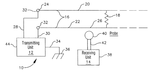
Figure 1 is a conceptual view of a fault locating device of the present
invention
operably positioned in relation to a paired line.
Figure 2 is a block diagram of the transmitting unit shown in the device of
Figure
1.
Figure 3 is a block diagram of the receiving unit shown in the device of
Figure
1.
Figure 4 is a conceptual view of an alternate pickup coil configuration having
utility in the fault location device of the present invention.
Figures 5a, 5b, 5c depict conceptualized operation of a synchronous detector
employed in the receiving unit of Figure 3.
Figure 6 is a conceptual cross-sectional view of a shielded cable, to which
the
fault location device of the present invention is applied, for detecting a
shield break.
-6-
CA 02239664 1998-06-04
DESCRIPTION OF PREFERRED EMBODIMENTS
Referring initially to Figure 1, a fault locating device of the present
invention is
shown and generally designated 10. The fault locating device 10 has two basic
components comprising a transmitting unit 12 and a receiving unit 14. The
fault
locating device 10 is operably positioned relative to a paired line 16, in
which it is
desired to locate a fault 18, such that the transmitting unit 12 engages a
first conductor
20 and a second conductor 22 of the paired line 16 at a transmission point 24
on the
paired line 16.
The fault locating device 10 of the present invention has general utility to
paired
lines employed in paired cables for a number of different applications,
including power
transmission and communications. As defined herein, a paired line is
substantially any
line having at least two continuous electrical conductors that, in the absence
of a fault,
are electrically insulated from one another. The two conductors can each be
solid or
braided wires, grounded or ungrounded and having parallel or spiral paths.
Alternatively, one conductor can be a wire and the other conductor can be a
conductive
tubular shield enclosing the wire. The above-recited definition of a paired
line
encompasses coaxial cable, shielded cable, and cable having more than two
conductors, wherein any two conductors of the cable may be deemed to define a
paired
line for purposes of the invention. For example, a paired line as defined
herein includes
a shielded cable having a shield and a conductor enclosed within the shield.
The fault
locating device 10 has particular utility to twisted paired lines employed in
paired cable
for telecommunications applications, including accessible paired cables, such
as aerial
paired cables, and inaccessible paired cables, such as buried paired cables.
A fault is defined herein as any unintended perturbation in the path of a
conductor that undesirably draws current therefrom, such as a short, an open,
a cross,
a ground, a split, or a shield break. The present fault locating device 10 is
applicable
to the location of many types of faults as generally defined above.
The receiving unit 14 is operably positioned proximal to a reception point 26
on
the paired line 16 that is between the transmission point 24 and the fault 18.
As such,
the receiving unit 14 preferably does not electrically contact the conductors
20, 22, but
is sufficiently proximal to the conductors 20, 22 to induce induced locator
and carrier
-7-
CA 02239664 1998-06-04
signals in the receiving unit 14 as will be described hereafter. The
transmission point
24 is preferably selected at a point on the paired line 16 where relatively
convenient
electrical access to the conductors 20, 22 is provided, such as a junction box
or other
splice location. Electrical communication is provided between the transmitting
unit 12
and the conductors 20, 22 by test leads 28, 30 extending from the transmitting
unit 12.
The test leads 28, 30 have electrically conductive connectors 32, such as
conventional
alligator clips or the like, on their ends which are removably connected to
the
conductors 20, 22. A ground lead 34 is also provided, connecting the
transmitting unit
12 in electrical communication with a ground 36.
As will be described in greater detail hereafter with respect to the method of
operation, the position of the transmission point 24, and correspondingly the
position
of the transmitting unit 12, are substantially fixed relative to the paired
line 16 during a
given fault locating sequence. In contrast, the position of the reception
point 26, and
correspondingly the position of the receiving unit 14, are variable along the
length of the
paired line 16 throughout a given fault locating sequence. Accordingly, the
receiving
unit 14 has a fully mobile, unanchored, portable configuration. The receiving
unit 14
is relatively compact and lightweight to render it manually transportable by a
single
operator. In the embodiment of Figure 1, the receiving unit 14 is shown to
comprise a
unitary housing 38 and a probe 40 positioned outside the housing 38. A
connective
member 42 extends between the probe 40 and the housing 38. The housing 38 is
preferably a hardened protective shell and the connective member 42 is
typically an
electrically conductive wire extending between the housing 38 and the probe
40,
functioning in a manner described hereafter. The connective member 42 may
further
include a flexible or rigid pole supporting the electrically conductive wire.
Although not
shown, the probe 40 can alternatively be positioned within the housing 38,
thereby
eliminating the connective member 42 external to the housing 38.
The specific components of the transmitting unit 12 are described with further
reference to the block diagram of Figure 2. Substantially all of the circuitry
of the
transmitting unit 12 is enclosed in a housing 44 (shown in Figure 1)
comprising a
hardened protective shell. The circuitry of the transmitting unit 12 includes
a power
source 46, a locator signal transmission circuit 48 and a carrier signal
transmission
_g_
CA 02239664 1998-06-04
circuit 50. As described above, the test leads 28, 30 extend from the
transmitting unit
12 and removably connect with the conductors 20, 22 to provide electrical
communication between the circuits 48, 50 and the paired line 16. The locator
signal
transmission circuit 48 is configured to generate and send locator signals
along the
conductors 20, 22 of the paired line 16 from the transmission point 24 toward
the
reception point 26. Included within the locator signal transmission circuit 48
is a locator
signal output 52, which in the present embodiment is a locator signal
oscillator. It is
apparent to the skilled artisan that alternate locator signal outputs are
possible within
the scope of the present invention. The locator signal transmission circuit 48
further
includes in series a locator signal driver 54, and a locator signal
transformer 56. The
outlet of the locator signal transformer 56 is segmented into a first outlet
winding 58 and
a second outlet winding 60 which are electrically coupled with the
transmission lines 28,
30, respectively. A center tap 62 is provided between the two outlet windings
58, 60.
The outlet line 64 of the locator signal output 52 is branched, with one
branch line 66
extending to the locator signal driver 54 as described above and the other
branch line
68 extending to the carrier signal transmission circuit 50.
The carrier signal transmission circuit 50 is configured to generate a carrier
signal, provide the carrier signal with modulated synchronization, and
transmit the
modulated carrier signal along the conductors 20, 22 of the paired line 16
from the
transmission point 24 toward the reception point 26. Included in series within
the
carrier signal transmission circuit 50 are a zero crossing detector 70, a
carrier signal
output 72, a carrier signal driver 74, and a carrier signal transformer 76. In
the present
embodiment, the carrier signal output 72 is a carrier signal oscillator. It is
apparent to
the skilled artisan that alternate carrier signal outputs are possible within
the scope of
the present invention. One outlet 78 of the carrier signal transformer 76 is
electrically
coupled with the center tap 62 of the locator signal transformer 56 and the
other outlet
80 of the carrier signal transformer 76 extends through the ground leads 34 to
ground
36 or to a cable shield (not shown), which functions as a ground.
The power source 46 is a DC power source included in the housing 44 of the
transmitting unit 12. The power source 46 supplies power to the components of
the
transmitting unit 12 enabling the functions thereof. The power source 46 is
preferably
_g_
CA 02239664 1998-06-04
a relatively small, lightweight battery pack, such as one or more dry-cell or
rechargeable
batteries (e.g., D-cell batteries).
It is noted that the zero crossing detector 70 can be omitted from the
transmitting
unit 12 without disabling operation of the transmitting unit 12, as will be
described
hereafter.
The specific components of the receiving unit 14 are described with further
reference to the block diagram of Figure 3. The probe 40 (shown in Figure 1 )
encloses
a pickup coil 82 electrically coupled with the circuitry of the receiving unit
14. The
pickup coil 82 has a balanced configuration which has specific utility for
locating faults
in an inaccessible paired line as will be described hereafter. It is
understood that
alternately configured pickup coils can be utilized, depending on the specific
application
of the fault locating device 10. The balanced pickup coil 82 is relatively
large, typically
having an elongated magnetic core or core of other geometry sufficient to meet
the
performance requirements of the receiving unit 14. The balanced pickup coil 82
includes a first coil segment 84 having a first coil outlet line 85 and a
second coil
segment 86 having a second coil outlet line 87. The first and second coil
outlet lines
85, 87 in cooperation with first and second receiving circuitry inlet lines
88, 89,
respectively, electrically couple the first and second coil segments 84, 86
with the
circuitry of the receiving unit 14. Male/female connectors 90a, 90b such as
conventional telephone jacks, are provided to reasonably connect the first and
second
coil outlet lines 85, 87 and the first and second receiving circuitry inlet
lines 88, 89,
respectively. The connectors 90a, 90b enable the substitution of alternately
configured
coils for the balanced coil 82, such as described hereafter.
The spacing between the first and second coil segments 84, 86 which is defined
as the distance between the midpoints of the segments 84, 86 is about equal to
one
half the length of the lay of the paired line 16, wherein the paired line 16
is shown to be
twisted and spiraled in the conventional manner of a telecommunications cable.
The
length of the lay for telecommunications cable is commonly about 36 inches and
the
current direction in each adjacent loop 91 of the lay differs by 180°.
Thus, the first and
second coil segments 84, 86 are phased due to the 18 inch spacing between the
coil
segments 84, 86 and the corresponding 36 inch length of the cable lay. The
pickup coil
-10-
CA 02239664 1998-06-04
82 further includes a center tap 92 positioned on a coil common 93, which
connects the
first and second coil segments 84, 86. A third coil outlet line 94 extends
from the center
tap 92 through a connector 90c, similar to those described above, to a
receiving unit
common 95.
The circuitry of the receiving unit 14 includes a power source 94, an induced
locator signal balancing/amplifying circuit 97, an induced locator signal
processing
circuit 98, an induced carrier signal processing circuit 100, and a capacitive
signal
processing circuit 102. The induced locator signal balancing/amplifying
circuit 97
provides an electrical pathway for noise pulling in the receiving unit 14. The
induced
locator signal balancing/amplifying circuit 97 comprises a first balancing
inlet pathway
104 and a second balancing inlet pathway 106 positioned in parallel. The first
balancing inlet pathway 104 and the second balancing inlet pathway 106 are
electrically
coupled with the first coil segment 84 and the second coil segment 86 through
the first
and second receiving circuitry inlet lines 88, 89, connectors 90a, 90b, and
first and
second coil outlet lines 85, 87, respectively. Each balancing inlet pathway
104, 106
provides an inlet to a balancing amplifier 108. The first balancing inlet
pathway 104
includes a pair of balancing resistors 11Oa, 11Ob and has a feedback line 112
electrically coupled with the outlet 114 of the balancing amplifier 108. The
second
balancing inlet pathway 106 also includes a pair of balancing resistors 116a,
116b and
a branch line 118. The branch line 118 is electrically coupled with a
balancing
potentiometer 120, enabling balance adjustment of the pickup coil 82.
The induced locator signal balancing/amplifying circuit 97 selectively
electrically
communicates with the induced locator signal processing circuit 98 through a
first
switch 122 at the outlet 114 of the balancing amplifier 108 downstream of the
branch
line 112. The induced locator signal processing circuit 98 provides an
electrical
pathway capable of producing an audible or visual fault indicator for an
operator in
response to a balanced induced locator signal. When the first switch 122 is
appropriately positioned, the balancing amplifier 108 of the induced locator
signal
balancing/amplifying circuit 97 is electrically coupled in series with a
variable gain
amplifier 124 and a band pass filter 126 of the induced locator signal
processing circuit
98. The outlet 128 of the band pass filter 126 splits into a real component
pathway 130
-11-
CA 02239664 1998-06-04
and a quadrature component pathway 132. The real component pathway 130
includes
in series a real synchronous detector 134 and a real low pass filter 136,
which lead to
a second switch 138. The quadrature component pathway 132 similarly includes
in
series a quadrature synchronous detector 140 and a quadrature low pass filter
142,
which lead to the second switch 138. The second switch 138 selectively
electrically
couples the real component pathway 130 or the quadrature component pathway 132
with an indicator output 144 of the induced locator signal processing circuit
98. The
indicator output 144 comprises in parallel a display 146 and an audio speaker
148,
having an associated output oscillator 150. The indicator output 144 enables
the
receiving unit 14 to communicate a fault indicator both visually and audibly
to an
operator of the device 10.
The induced locator signal processing circuit 98 is in electrical
communication
with the induced carrier signal processing circuit 100 by means of a phase
shifter 152
electrically coupled with the outlet 154 of the induced carrier signal
processing circuit
100. The outlet 156 of the phase shifter 152 splits into a real
synchronization pathway
158 and a quadrature synchronization pathway 160. The real synchronization
pathway
158 has a real synchronous oscillator 162 that is electrically coupled with
the real
synchronous detector 134. The quadrature synchronization pathway 160 similarly
has
a quadrature synchronous oscillator 164 that is electrically coupled with the
quadrature
synchronous detector 140. Although the real and quadrature synchronous
oscillators
162, 164 are shown herein to be separate components, it is apparent to the
skilled
artisan that the oscillators 162, 164 can be replaced by a single oscillator
or a
microcontroller delivering real and quadrature synchronization signals in the
same
manner as described above.
The induced carrier signal processing circuit 100 provides an electrical
pathway
for producing and communicating a demodulated synchronization signal to the
induced
locator signal processing circuit 98. Included in series within the induced
carrier signal
processing circuit 100 are an induced carrier signal amplifier/receiver 166,
an induced
carrier signal limiter 168 and a synchronization signal output 170. In the
present
embodiment, the synchronization signal output 170 is a carrier signal
demodulator. It
is apparent to the skilled artisan that alternate synchronization signal
outputs are
-12-
CA 02239664 1998-06-04
possible within the scope of the present invention. As used herein, the term
"limiter"
is defined to encompass a conventional limiter or, in the alternative, an
automatic gain
control. The inlet 172 of the carrier signal amplifier/receiver 166 is
electrically coupled
with the first coil segment 84 via the receiving circuitry inlet line 88 and a
receiving
circuitry outlet line 174. The outlet 154 of the synchronization signal output
170 is
electrically coupled with the inlet 178 of the phase shifter 152.
The capacitive signal processing circuit 102 selectively electrically
communicates
with the induced locator signal processing circuit 98 through the first switch
122. The
capacitive signal processing circuit 102 in cooperation with the induced
locator signal
processing circuit 98 provides an electrical pathway capable of producing an
audible
or visual fault indicator for an operator in response to a capacitive signal.
The
capacitive signal processing circuit 102 includes in series a ground 179, a
ground
pickup 180 and a capacitive signal amplifier 182. If the housing 38 of the
receiving unit
14 is electrically conductive, the ground pickup 180 is simply the housing 38.
If the
housing 38 is not electrically conductive, the ground pickup 180 can be
provided by an
electrical conductor, such as a metallic shield (not shown) contained within
the housing
38. The ground pickup 180 is electrically coupled with the body of an operator
(not
shown) to provide the ground 179 and corresponding ground reference when the
operator is standing on the earth. When the first switch 122 is appropriately
positioned,
the capacitive signal amplifier 182 of the capacitive signal processing
circuit 102 is
electrically coupled with the variable gain amplifier 124 and band pass filter
126 of the
induced locator signal processing circuit 98.
The power source 96 is a DC power source included in the housing 38 of the
receiving unit 14. The power source 96 supplies power to the components of the
receiving unit 14 enabling the functions thereof. The power source 96 is
preferably a
relatively small, lightweight battery pack, such as described above with
respect to the
transmitting unit 12.
It is noted that the carrier signal amplifier/receiver 166 is shown and
described
herein as integrated into a single structure. In practice, this integrated
structure can be
separated into discrete structural components performing the same functions
ascribed
to the integrated structure in a manner apparent to the skilled artisan.
-13-
CA 02239664 1998-06-04
Referring to Figure 4, an alternate nonbalanced pickup coil 186 is shown,
which
is substituted for the 82 balanced pickup coil. The nonbalanced pickup coil
186, which
is a relatively small contact coil with a single coil segment and two outlets
190, 192, has
specific utility for locating faults in an accessible paired line 16. The
first outlet 190 is
electrically coupled with the first balancing inlet pathway 104 through the
connector 90a
and the second outlet 192 is electrically coupled with the receiving unit
common 95
through the connector 90c, while the second balancing inlet pathway 106 is
open
circuited. As a result, the balancing potentiometer 120 is rendered
nonfunctional, while
the balancing amplifier 108 functions as an unbalanced input amplifier.
Method of Operation
Operation of the fault locating device 10 is initially described with
reference to
Figures 1-3. The method of operation is initiated by identifying a paired line
16 that is
believed to contain the fault 18. For purposes of illustrating a first
embodiment of the
method of the present invention, the fault 18 is characterized as a resistance
fault and,
more particularly, as a short fault. The paired line 16 is typically up to
about 5000
meters in length, although practice of the present fault locating method
applies to
paired lines 16 of substantial greater length. An operator fixably positions
the
transmitting unit 12 at a transmission point 24 on the paired line 16. The
test leads 28,
30 are removably connected to the first and second conductors 20, 22 at the
transmission point 24 and the ground lead 34 is removably connected to ground
36 or
the cable shield (not shown). The DC power source 46 energizes the locator
signal
output 52 and locator signal driver 54 of the locator signal transmission
circuit 48, which
generate an AC locator signal in the form of a variable voltage sine wave. The
locator
signal is delivered to the locator signal transformer 56 where the voltage of
the locator
signal is adjusted to a predetermined level. The first and second outlet
windings 58,
60 of the locator signal transformer 56 convert the locator signal to a first
locator signal
and a second locator signal, respectively, which have substantially identical
voltage, but
opposite polarity. The resulting first and second locator signals are
introduced into the
first and second conductors 20, 22, respectively, through the test leads 28,
30,
respectively.
-14-
CA 02239664 1998-06-04
The variable voltage sine wave of the locator signal output 52 is also
transmitted
to the carrier signal transmission circuit 50 where the sine wave is converted
to a
square wave in the zero crossing detector 70. The square wave signal is then
modulated in the carrier signal output 72, which is a voltage control
oscillator, by
frequency shift key modulation to produce a carrier signal having modulated
synchronization. The resulting carrier signal is fed through the carrier
signal driver 74
to the carrier signal transformer 76 where the voltage of the carrier signal
is modified.
The carrier signal is then introduced into each of the conductors 20, 22 via
the outlet
78 of the carrier signal transformer 76, the center tap 92, the outlet
windings 58, 60,
and the test leads 28, 30 of the locator signal transmission circuit 48.
It is understood that the present invention can alternatively be practiced
using
a sine wave carrier signal rather than the square wave carrier signal
described above.
In accordance with this embodiment, the zero crossing detector 70 is omitted
from the
fault locating device 10 and the induced carrier signal processing circuit 100
is
configured to process a sine wave, rather than a square wave, by varying the
frequency
of the carrier signal output 72 sinusoidally, in a manner readily apparent to
the skilled
artisan, in place of frequency shift key modulation.
The voltage and frequency of the locator and carrier signals are preferably
limited to ranges that satisfy desirable performance criteria of the fault
locating device
10. In particular, the voltage and frequency ranges of the locator signals are
preferably
selected at the upper end to avoid excessive carry-by of the locator signal on
the paired
line 16. Generally, a signal having both a very low voltage and a very low
frequency
avoids significant carry-by. Such a signal, however, may fail to satisfy other
performance criteria of the device 10, lacking sufficient voltage to exceed
the
background noise or sufficient frequency to enable detection. If the frequency
of the
locator signals is raised to improve the detectability thereof, the locator
signals may
become overly susceptible to carry-by. Alternatively, if the voltage of the
locator signals
is raised to overcome the background noise, excessive battery power may become
necessary.
Selection of the voltage and frequency of the locator signals may require a
balancing of competing factors to achieve a fully-portable fault locating
device 10
-15-
CA 02239664 1998-06-04
having detectable locator signals that exceed the background noise on the
paired line
16 while avoiding the effects of excessive carry-by. Achievement of these
performance
criteria is facilitated by noise nulling means that reduce the noise induced
in the pickup
coil 82, and by synchronization circuitry that mitigates the impact of carry-
by, as
described hereafter. As such, the frequency of the locator signals is
typically selected
in the RF, audible, or sub-audible range. A preferred range is less than about
20,000
Hz, more preferably in a range between about 20,000 Hz and about 1 Hz, and
most
preferably in a range between about 1,500 and about 10 Hz. The voltage of the
locator
signals is typically selected in a range between about 1 volt and about 150
volts and
on each conductor 20, 22, and preferably at a value of about 25 volts. The
frequency
of the induced locator signals is substantially identical to that of the
transmitted locator
signals, but the voltage is typically selected in a range between about 0.1
microvolt and
1000 microvolts and preferably at a value of about 10 microvolts, which is
generally
greater than ambient noise. The carrier signal has a frequency range greater
than
about 5 kHz, and preferably between about 5 kHz and about 100 kHz. The carrier
signal typically has a voltage below about 150 volts within the prescribed
frequency
range and preferably has a voltage of about 25 volts.
The present method of locating the fault 18 proceeds by positioning the probe
40 of the receiving unit 14 proximal to a selected reception point 26 on the
paired line
16, preferably between the transmission point 24 and the fault 18. The actual
position
of the reception point 26 is variable, rather than fixed, during operation of
the fault
locating device 10. The reception point 26 is preferably positioned near the
transmission point 24 during initial operation of the device 10. The reception
point 26
is then incrementally repositioned away from the transmission point 24 as
operation of
the device 10 proceeds. The relative distance between the probe 40 and the
conductors 20, 22 at any given reception point 26 is termed the induction
distance. The
maximum allowable induction distance is a function of the power output of the
transmitting unit 12, the size and configuration of the pickup coil, and the
voltage of the
locator and carrier signals in the conductors 20, 22. A typical maximum
allowable
induction distance is up to about 1 meter using the relatively large balanced
pickup coil
82 for inaccessible buried paired cable and up to about 0.06 meters using the
relatively
-16-
CA 02239664 1998-06-04
small unbalanced pickup coil 186 for accessible paired cable.
The locator and carrier signals travel along the conductors 20, 22 to the
reception point 26, where the locator and carrier signals induce induced
locator and
carrier signals in the balanced pickup coil 82 of the receiving unit 14. Since
the spacing
between the first and second coil segments 84, 86 is equal to one half the
length of the
lay of the paired line 16, the balanced pickup coil 82 sees two adjacent half
lengths of
the lay of the paired line 16 at any given reception point 26. Thus, a first
induced
locator signal is induced in the first coil segment 84 and a second induced
locator signal
of opposite polarity is induced in the second coil segment 86. The first and
second coil
segments 84, 86 are electrically coupled with the first and second balancing
inlet
pathways 104 and 106 to receive the induced locator signals of opposite
polarity and
sum the signals in the balancing amplifier 108. In contrast, background noise
from
sources such as nearby power lines (not shown) not having a 36 inch lay length
induces induced noise signals of the same polarity in each coil segment 84,
86, which
cancel in the balancing amplifier 108. Consequently, the balancing amplifier
108
outputs a balanced induced locator signal in response to the first and second
induced
locator signals, but is unresponsive to induced noise signals.
The specific configuration of the induced locator signal balancing/amplifying
circuit 97 enhances the ability of the device 10 to reject interfering signals
from the
surroundings, while processing desired signals from the paired line 16. In
particular,
the induced locator signal balancing/amplifying circuit 97 is perfectly
balanced when the
first resistance ratio, defined as the resistance of the balancing resistor
110a divided
by the resistance of the balancing resistor 110b, exactly equals the second
resistance
ratio, defined as the resistance of the balancing resistor 116a divided by the
sum of the
resistances of the balancing resistor 116b and the balancing potentiometer
120. The
resistances of the balancing resistor 116b and the balancing potentiometer 120
are
selected such that the induced locator signal balancing/amplifying circuit 97
is in perfect
balance when the balancing potentiometer 120 is positioned at the center of
its range.
If an extraneous signal induces induced noise signals of equal polarity, but
differing
voltages, in the respective coil segments 84, 86, the balancing potentiometer
can be
offset to compensate for the voltage difference. As a result, the two induced
noise
-17-
CA 02239664 1998-06-04
signals can be summed to zero and canceled in the balancing amplifier 108 even
when
the voltages of the induced noise signals in the coil segments 84, 86 are not
identical.
The balanced induced locator signal is transmitted from the induced locator
signal balancing/amplifying circuit 97 to the induced locator signal
processing circuit 98,
while the induced carrier signal is transmitted from the pickup coil 82 to the
induced
carrier signal processing circuit 100. Specifically, the induced carrier
signal is
transmitted via the receiving circuitry outlet line 174 to the carrier signal
amplifier/receiver 166, which amplifies and filters the induced carrier
signal. The carrier
signal limiter 168 subsequently limits the amplitude of the amplified signal.
The
synchronization signal output 170 demodulates the induced carrier signal,
producing a
synchronization signal that is transmitted from the synchronization signal
output 170 to
the phase shifter 152 of the induced locator signal processing circuit 98. If
necessary,
the phase shifter 152 corrects any phase irregularities in the synchronization
signal
caused by demodulation. The phase shifter 152 has a split outlet 156, such
that the
synchronization signal is transmitted in parallel to the real synchronous
oscillator 162
and the quadrature synchronous oscillator 164. The real synchronous oscillator
162
produces a real synchronization signal that is in phase with the
synchronization signal
and transmits the real synchronization signal to the real synchronous detector
134. The
quadrature synchronous oscillator 164 similarly produces a quadrature
synchronization
signal that is 90° out of phase with the synchronization signal and
transmits the
quadrature synchronization signal to the quadrature synchronous detector 140.
The balanced induced locator signal is transmitted to the induced locator
signal
processing circuit 98 through the first switch 122, which the operator has
manually
placed in an up position corresponding to a resistive short fault detection
mode of
operation. The voltage of the balanced induced locator signal is further
amplified in the
variable gain amplifier 124 and, if desired, adjusted for differences in the
signal due to
fault resistance losses. The band pass filter 126, which is tuned to the
relatively low
frequency of the balanced induced locator signal, rejects extraneous signals
from the
output of the variable gain amplifier 124 that have surrounding frequencies.
In
particular, the band pass filter 126 attenuates interference from 50/60 Hz
signals that
are magnetically induced onto the paired line 16 by adjacent power lines.
-18-
CA 02239664 1998-06-04
The balanced induced locator signal, which is output from the band pass filter
126, is split and fed in parallel to the real component pathway 130 and the
quadrature
component pathway 132 of the induced locator signal processing circuit 98. The
balanced induced locator signal may be characterized as comprising a real
component
and a quadrature component, one or both of which may be present in the
balanced
induced locator signal at any given time during operation of the device 10.
The real
component is resistive current that is in phase with the voltage of the
locator signal
generated in the transmitting unit 12. The quadrature component is capacitive
current
that leads the voltage of the locator signal generated in the transmitting
unit 12 by 90°.
Accordingly, the real component pathway 130 and quadrature component pathway
132
detect and segregate the respective components of the balanced induced locator
signal, based on phase synchronization. The real synchronous detector 134
utilizes
the real synchronization signal to detect only the presence of the real
component, which
corresponds to the current of the locator signal flowing through the fault
resistance, and
to reject any carry-by occurring due to current flow into pair capacitance or
conductor-
to-ground capacitance. The quadrature synchronous detector 140 conversely
utilizes
the quadrature synchronization signal to detect only the presence of the
quadrature
component, which corresponds to current flow into capacitance, and to reject
the
current flowing through the fault resistance or leakage on the conductor. The
real low
pass filter 136 filters the rectified DC signal from the real synchronous
detector 134,
allowing a narrowing of the circuit bandwidth to more effectively filter out
50/60Hz
signals and other extraneous signals having undesired frequencies. The
quadrature
low pass filter 142 similarly filters the rectified DC signal from the
quadrature
synchronous detector 140.
Since the present fault 18 is a resistance fault, the operator has manually
placed
the second switch 138 in an up position, enabling the resistive short fault
detection
mode of operation. The second switch 138 electrically couples the real low
pass filter
136 with the indicator output 144 of the induced locator signal processing
circuit 98.
The real component is transmitted to the indicator output 144 which operates
in
correspondence with the presence and magnitude of the real component to
communicate a fault indicator to the operator. In particular, the output
oscillator 150,
-19-
CA 02239664 1998-06-04
which is an audio voltage control oscillator, and the audio speaker 148
generate an
audible correlation of the real component in the form of a continuous audible
tone
having an intensity or frequency directly related to the presence and voltage
magnitude
of the real component. As the magnitude of the real component increases, the
intensity
or frequency of the tone generated by the speaker increases. Correspondingly,
as the
magnitude of the real component decreases, the intensity or frequency of the
tone
generated by the speaker decreases.
When the receiving unit 14 approaches the resistive short fault 18 from the
transmission point 24, the receiving unit 14 detects voltage due to current
flow in the
fault resistance. The magnitude of this voltage may rise and fall and reverse
in polarity
as the pickup coil 82 is moved along the paired cable containing the paired
line 16 due
to the twist of the conductors 20, 22 and the spiraling of the paired line 16
within the
paired cable, but will remain continuous before the fault 18 is reached.
Polarity
changes can be communicated to the operator by a change in a characteristic of
the
audible tone generated by the output oscillator 150 in correspondence with
polarity
changes. In any case, when the receiving unit 14 passes the fault 18, the
receiving unit
14 no longer detects any voltage. Thus, the fault 18 in the paired line 16 is
located by
moving the receiving unit 14 along the paired line 16 away from the
transmission point
24 in the direction of the fault 18 to establish incrementally new reception
points 26.
The fault 18 is precisely located at the point on the paired line 16 where the
intensity
or frequency of the tone from the speaker 148 is strong followed by an abrupt
drop in
the intensity or frequency of the tone as the receiving unit 14 continues
along the paired
line 16. The display 146 provides a quantitative visual verification of the
information
communicated to the operator by the speaker 148. The display 146 is a visual
correlation of the magnitude of the real component in the form of either an
analog or
a digital readout of the values of the magnitude as the receiving unit 14 is
moved along
the paired line 16.
Although voltage is selected herein as the characteristic of the induced
locator
signal which is quantified by the indicator output 144 to enable fault
location, it is
apparent to the skilled artisan that an alternate characteristic of the
induced locator
signal can be selected for quantification, such as phase shift, to enable
fault location
-20-
CA 02239664 1998-06-04
within the scope of the present invention.
The principle by which the real synchronous detector 134, and correspondingly
the quadrature synchronous detector 140, operate is described with reference
to Figure
5a, 5b and 5c. Operation of the real synchronous detector 134 in association
with the
fault locating device 10 of Figure 1 is the functional equivalent of a circuit
194 shown
in Figure 5a. The circuit 194 has a switch 196 that is opened and closed in
synchronism with the induced locator signal in the receiving unit 14. The
circuit 194
further includes a series resistor 198 and, in parallel, a resistor 200, a
capacitor 202
and an amplifier 204 such that the output voltage of the circuit 194 is the
average input
voltage of the circuit 194 when the switch 196 is closed. The switch 196 is
opened and
closed as shown in Figure 5b by the switch waveform 206. Figure 5c shows the
input
voltage waveform of the circuit 194 as the sum of two distinct waveforms, a
resistance
current waveform 208 and a capacitance current waveform 210.
By opening and closing the switch 196 in synchronism with the input voltage
waveform, in accordance with the relationship shown in Figures 5b and 5c, the
capacitance current waveform 210 of the carry-by leads the resistance current
waveform 208 by 90°, thereby averaging to zero as indicated by the
shaded area under
the capacitance current waveform 210 of Figure 5c. In contrast, the entire
fault
resistance current waveform 208 is in phase with the induced locator signal
and the
switch waveform 206, thereby enabling detection of the resistance fault.
Synchronous operation of the receiving unit 14 and transmitting unit 12 in
conjunction with the use of locator signals having a relatively low frequency
enables the
effective location of faults having resistances above 50 kohms without a
significant
impact from carry-by, even in relatively long paired lines 16 having lengths
of 5000
meters or more. Low frequency operation tends to decrease carry-by because
lowering
the frequency of the locator signal increases the capacitive reactance of the
paired line
16, reducing the magnitude of locator signal current flow past the fault 18.
The low
frequency locator signal has the added advantage of exhibiting substantially
less
attenuation over length of the paired line 16 than would a higher frequency
locator
signal. Synchronous detection further enables the operator to observe changes
in
polarity due to twisting of the conductors 20, 22. This permits the operator
to
-21-
CA 02239664 1998-06-04
differentiate between carry-by and the locator signal in the presence of
unbalanced
conductor faults and ground faults both of which are more susceptible to carry-
by than
balanced conductor faults.
In another embodiment of the present method, the fault 18 is characterized as
an open fault, which is generally defined herein to include a splice
containing a bridge
tap, i.e., a conductor bridged onto the main conductor. The operator manually
repositions the second switch 138 in a down position, enabling the open fault
detection
mode of operation. The second switch 138 electrically couples the quadrature
low pass
filter 142 with the indicator output 144 of the induced locator signal
processing circuit
98. The quadrature low pass filter 142 filters the rectified DC signal from
the
quadrature synchronous detector 140 in substantially the same manner as the
real low
pass filter 136. The quadrature component is transmitted to the indicator
output 144.
The indicator output 144 operates in correspondence with the presence and
magnitude
of the quadrature component in substantially the same manner as described
above with
respect to the real component to locate the position of the open fault on the
paired line.
Location of the bridged tap is alternately enabled because the bridged
conductor draws
capacitive currents, which are monitored when the device 10 is configured to
locate
open faults. Then the receiving unit 14 passes a splice in the paired line 16
containing
a bridged tap, there is an abrupt drop in the magnitude of capacitive current
flowing
through the paired line 16, producing a corresponding abrupt drop in the
audible or
visual fault indicator.
In an alternate method of operating the fault locating device 10, a cable
shield
break is located in a cable having at least one conductor surrounded by a
shield.
Referring to Figure 6, a cable 212 is shown, to which the present method of
locating a
shield break is applicable. The cable 212 has a shield 214 and at least one
continuous
concentric wire enclosed thereby as a conductor 216. It is understood that
additional
continuous wires may also be present within the shield 214 to provide the
cable 212
with multiple conductors. Referring additionally to Figure 3, the method is
performed
by installing the unbalanced pickup coil 186 of Figure 4 in the receiving unit
14 and
manually placing the first switch 122 in the down position to connect the
capacitive
signal processing circuit 102 with the induced locator signal processing
circuit 98. The
-22-
CA 02239664 1998-06-04
conductor 216 is grounded to the cable shield 214 at both ends (not shown) of
the
cable 212 and a locator signal is sent by the transmitting unit 12 along the
conductor
216 of the cable 212. When the shield 214 is broken, the locator signal
flowing in the
conductor 216 generates a longitudinal voltage on the cable shield 214 which
is
normally shorted to earth at each shield ground connection. However, in the
case of
a shield break, the voltage builds up on the shield 214 at the point of the
break.
The unbalanced pickup coil 186, which is a capacitive pickup functioning as a
capacitor, impresses a capacitive signal onto the receiving unit common 95
through the
third coil outlet line 94 in response to the voltage on the cable shield 214
as the
receiving unit 14 is moved along the length of the cable 212. It is noted that
the
receiving unit common 95 is floating ungrounded within the insulated receiving
unit
housing 44. The ground pickup 180 is grounded, for example, by capacitively
coupling
with the operator, who in turn is coupled with the earth through his feet.
Accordingly,
the capacitive signal that appears in the pickup coil 186 is received by the
capacitive
amplifier 182 via the receiving unit common 95. The capacitive amplifier 182
amplifies
the difference between the capacitive signal and the ground reference received
via the
ground pickup 180. The resulting differential capacitive signal is sent to the
induced
locator signal processing circuit 98 for evaluation. Since the capacitive
signal reverses
polarity across the shield break (not shown) and is at a maximum level when
the
receiving unit 14 is adjacent to the shield break, the speaker 148 and/or
display 146
communicate the level of the differential capacitive signal to the operator
along the
length of the cable 212, thereby enabling precise location of the shield break
within the
cable 212.
Although the unbalanced pickup coil 186 is described as the capacitive pickup
herein, the present invention is not so limited. It is apparent to the skilled
artisan that
substantially any component functioning as a capacitive plate can serve as the
capacitive pickup within the scope of the present invention.
While the forgoing preferred embodiments of the invention have been described
and shown, it is understood that alternatives and modifications, such as those
suggested and others, may be made thereto and fall within the scope of the
invention.
-23-