Note: Descriptions are shown in the official language in which they were submitted.
CA 02239912 1998-07-28
DIGITA~ ENGINE ANALYZER
BACKGROUND OF THE INVENTION
FIELD OF THE INVENTION
This invention relates to methods and apparatus for
electronically diagnosing and analyzing the performance of
internal combustion engines. The invention relates
particularly to digital engine analyzers of the type which
display digitized information on an oscilloscope screen.
DESCRIPTION OF THE PRIOR ART
The present invention is an improvement of the digital
engine analyzer disclosed in U.S. patent no. 4,800,378. One
of the waveforms commonly analyzed in engine analyzers of
that type is the secondary ignition pattern, which has a
distinctive shape. The pattern includes a high-amplitude
spiXe of very short rise and fall times at the beginning of
the cylinder power stroke, caused by the buildup of voltage
across the spark plug just prior to its firing; a plateau
region of medium amplitude, which is the "burn time" when
the spark plug is actually firing; and an oscillatory or
"ringing" portion after termination of the spark plug
firing. It will be appreciated that the power stroke is the
movement of the piston away from the spark plug in response
to combustion of the fuel, thereby delivering power to the
crankshaft.
Heretofore the spark plug ~urn time has rarely been
used as a diagnostic aid. However, useful diagnostic
information can be g,ained by determining the spark plug burn
time, and particularly by comparing the spark plug burn
times of the several cylinders. For example, short burn
times may be indicative of fouled plugs and/or high
resistance in the secondary of the ignition. Comparisons of
burn times can determine if one or more cylinders may have
faulty spark plugs and/or high resistance in the ignition
components.
It is known to measure the spark plug burn time, one
system for dolng so being disclosed in U.S. patent no.
4,291,393. But such prior art systems simply display
numerical data for the spark plug burn times, which ~akes it
CA 02239912 1998-07-28
difficult to readily compare the burn times of the several
cylinders. Furthermore, such systems require the use of
input signals from both the primary and the secondary of the
ignition coil in order to derive the burn time information.
One of the principal diagnostic techniques utilized in
prior engine analyzers is the display in kilovolts of the
peak voltage across the spark plug for each cylinder firing.
In the aforementioned U.S. patent no. 4,300,378, this
information is displayed in a number of ways, viz., a
display of the secondary waveform itself, a bar graph of the
peak values for the several cylinders, and the display of
numerical minimum and ~ximum values for each cylinder. But
none of these techniques permits the analysis of the peak
voltage performance of a single cylinder over time,
independently of the other cylinders.
Another diagnostic technique used in prior engine
analyzers is cylinder shorting, i.e., shorting out the
ignition voltage to a selected cylinder. The purpose of
cylinder shorting is to determine the contribution of each
individual cylinder to the overall power output of the
engine by successively shorting, or preventing operation of,
selected cylinders and noting the effect on the speed of the
engine. If the cylinder were contributing no power, then
the shorting of that cylinder would not decrease the engine
speed. If, on the other hand, the individual cylinder being
shorted were a normal contributor to the overall power, then
the speed of the engine would drop in response to the
shorting. If each individual cylinder contributed the same
amount to the overall power, then the shorting of each
cylinder would result in substantially the same speed drop.
In modern computer-controlled engines with catalytic
converters it is difficult and potentially harmful to short
out cylinders. Indeed, engine manufacturers specifically
warn against the use of this technique. Accordingly, at
least one prior system has obtained an indication of the
cylinder-by-cylinder power contribution or power "balancP"
CA 02239912 1998-07-28
without shorting the cylinders, by means of measuring the
variations in firing times between the cylinders. The
system provides a bar graph of the variations in firing
times between the cylinders. But this display shows the
time variation for each firing and, therefore, can
experience considerable flutter over several engine cycles,
making it difficult to read.
In a digital engine analyzer, the analog engine signals
are converted into digital information by sampling the
analog waveform at a predetermined rate and generating
digital representations of the sample values. That digital
information is stored and then displayed on the oscilloscope
screen. The oscilloscope is a cathode-ray tube, and the
display thereon consists of a multiplicity of dots arranged
in horizontal rows with a predetermined number of dots in
each row, this number representing the maximum number of
samples which can be simultaneously displayed across the
screen, which places an upper limit on the resolution of the
waveform display. This is not a problem if the amplitude of
the analog waveform is relatively constant over time or the
rate of change thereof is not great. However, during those
portions of the waveform containing very rapid rise and fall
times, such as during the spike portion at the beginning of
the cylinder ignition waveform pattern, it is difficult or
impossible to faithf-ully represent the actual waveform on a
digital oscilloscope wherein an entire cylinder period is to
be displayed.
This problem can be solved by increasing the sampling
rate, but if all the samples are displayed this would
prevent an entire cylinder period from being displayed on
the screen. In the aforementioned U.S. patent no.
4,800,378, the spike portion of the cylinder ignition
waveform is displayed by capturing the analog peak value and
digitizing it and then later inserting that value in the
displayed waveform. But the insertion doesn't occur until
the following engine cycle at the earliest, and a new peak
CA 02239912 1998-07-28
is captured only once every several engine cycles, depending
on engine speed, so that the displayed waveform is not a
true "live" waveform. Furthermore, the peak value might get
inserted at the wrong point, resulting in distortion of the
waveform.
Most modern automobile engines have on-board computers
which control and/or monitor a number of different engine
parameters and which produce a serial data stream indicating
the status of monitored parameters. This data stream may be
accessed through the Assembly Line Data Link (ALDL)
connector on the engine. Hand-held diagnostic instruments,
known as scanners, are adapted to plug into the ALDL
connector and access the serial data stream and interpret
and display the information. But such scanners have very
limited displays.
U.S. patent no. 4,602,127 discloses the concept of
interfacing such a scanner with an engine analyzer so that
all of the parameter data available to the scanner can be
simultaneously displayed on the cathode-ray tube of the
analyzer, but the patent does not disclose any means for
accomplishing this result. Furthermore, the scanner must be
utilized close to the engine, while the engine analyzer may
be remotely located and, therefore, it may be difficult for
the operator to read the engine analyzer display while at
the same time operating the scanner controls.
SUMMARY OF T~E INVENTION
It is a general object of the present invention to
provide an improved digital engine analyzer which avoids the
disadvantages of prior analyzers while affording additional
structural and operating advantages.
An important feature of the invention is the provision
of a digital engine analyzer which is of improved construc-
tion, permitting the performance of unique diagnostic tests
and providing simplified and/or improved performance of
standard diagnostic tests.
CA 02239912 1998-07-28
A significant feature of the invention is the provision
of an analyzer of the type set forth, which provides a
display of spark plug burn time information which permits
ready comparison of the burn times of the several cylinders.
In connection with the foregoing feature, another
feature of the invention is the provision of an analyzer of
the type set forth, which derives spark plug burn time
information from only a single analog input signal.
Yet another feature of the invention is the provision
of an analyzer of the type set forth which provides for a
historical display of the peak ignition voltage values for a
selected cylinder over a number of engine cycles.
In connection with the foregoing feature, another
feature of the invention is the provision of an analyzer of
the type set forth, which provides a continuously updated or
running graphical display of the historical peak voltage
data.
Still another feature of the invention is the provision
of an analyzer of the type set forth, which provides a
relatively stable display of cylinder time balance
information, so as to give an indication of cylinder-by-
cylinder power contribution without shorting the cylinders.
Another feature of the invention is to provide a
digital analyzer of the type set forth, which permits a
substantially accurate representation of portions of an
analog waveform having very short rise and fall times, while
at the same time permitting an entire cylinder period of the
waveform to be displayed on the screen.
In connection with the foregoing feature, it is another
feature of the invention to provide an analyzer of the type
set forth, which is capable of switching into a high
resolution mode for a short period of time sufficient to
relatively accurately reproduce the steep-sloped portion of
the waveform.
It is another feature of the invention to provide an
analyzer of the type set forth which interfaces with a
CA 02239912 1998-07-28
hand-held controller, such as a scanner adapted for connection
with a vehicle on-board computer, and whlch permlts the
scanner control functlons to be effected from the analyzer.
In accordance wlth the present lnventlon, there is
provided ln a system for analyzing the relative performance of
different cylinders of a multiple cylinder internal combustion
engine in which all of the cylinders are fired in a
predetermined firing order during each engine cycle, the
improvement comprising: sensing means coupled to the engine
for sensing the cylinder firings and producing a firing signal
in response to each firlng, processing means operating under
stored program control and coupled to said sensing means and
responsive to said firlng signals for calculatlng for each
cylinder a value representing lts cylinder tlme period where
the cylinder time period of a cyllnder is the time between the
flring of that cylinder and the firing of the next cylinder in
the firing order, said processing means including means for
calculating an overall average of the cylinder time period
values for all of the cylinders and for calculating the
2~ percentage difference between the cylinder time period value
for each cylinder and the overall average, and display means
coupled to said processing means for displaying for each
cyllnder the percentage difference between the cyllnder time
period value for that cylinder and the overall average.
In accordance with another aspect of the invention,
there is provided in a system for analyzing the relative
performance of different cylinders of a multiple cylinder
62739-238E
CA 02239912 1998-07-28
6a
internal combustlon englne ln which all of the cylinders are
fired in a predetermlned flrlng order durlng each englne
cycle, the lmprovement comprlsing senslng means coupled to
the englne for senslng the cyllnder firings and producing a
flrlng slgnal ln response to each flrlng, processlng means
operatlng under stored program control and coupled to sald
sensing means and responsive to said firing slgnals for
calculatlng the cyllnder time period for each cyllnder where
the cyllnder tlme period of a cyllnder ls the time between the
flrlng of that cyllnder and the flrlng of the next cyllnder ln
the firing order, memory means for storing for each cylinder
the cylinder tlme perlods calculated durlng a plurallty of
consecutlve englne cycles, sald processlng means lncludlng
means for calculatlng for each cyllnder the average value of
the stored cyllnder tlme perlods, sald memory means lncludlng
means for storlng sald average values for each cyllnder, sald
processlng means lncludlng means for calculatlng the overall
average of sald cyllnder average values and for calculatlng
the percentage dlfference between the average value for each
cyllnder and the overall average, and dlsplay means coupled to
sald processlng means and to sald memory means for displaylng
for each cyllnder the percentage dlfference.
In accordance wlth another aspect of the lnventlon,
there ls provlded a method of analyzlng the relatlve
performance of different cyllnders of a multiple cylinder
lnternal combustion englne ln whlch all of the cyllnders are
flred ln a predetermlned flrlng order durlng each englne
62739-238E
CA 02239912 1998-07-28
6b
cycle, the method comprislng the steps of: detecting the
firing of each cyllnder, calculating for each cylinder a value
representing its cylinder time period where the cylinder time
period of a cylinder is the time between the firing of that
cylinder and the firing of the next cylinder in the firing
order, calculating an overall average of the cylinder time
period values for all of the cylinders, calculating the
percentage difference between the cylinder time period value
for each cylinder and the overall average, and displaying the
percentage difference for each cylinder.
The invention consists of certain novel features and
a combination of parts hereinafter fully described,
illustrated in the accompanying drawings, and particularly
pointed out in the appended claims, it being understood that
various changes in the details may be made without departing
from the spirit, or sacrificing any of the advantages of the
present inventlon.
BRIEF DESCRIPTION OF THE DRAWINGS
For the purpose of facilitating an understanding of
the invention, there is illustrated in the accompanying
drawings a preferred embodiment thereof, from an inspection of
which, when considered in connection with the following
description, the invention, its construction and operation,
and many of its advantages should be readily understood and
appreciated.
FIG. 1 is a front elevational view of an engine
analyzer constructed in accordance with and embodying the
62739-238E
CA 02239912 1998-07-28
6c
features of the present inventlon;
FIG. lA is an enlarged view of the main keyboard of
the analyzer of FIG. 1;
FIG. Z is a view, partially in elevation and
partially ln perspective, of the englne analyzer of FIG. 1,
showing the lead connections for testlng an ignitlon system
wlth a remote coll;
FIG. 3 is a view similar to FIG. 2, illustrating the
lead connections for testing an integral-coil type ignltion
system;
FIG. 4 is a functional block diagram of the
circuitry of the engine analyzer of FIG. 1;
FIG. 5 is a partially schematic and partially block
diagram of the power supply system for the engine analyzer of
FIG. 1;
62739-238E
CA 02239912 1998-07-28
FIG. 6 is a partially schematic and partially block
diagram of the analog circuits of the engine analyzer
circuitry of FIG. 4;
FIG. 7 is a block diagram of the digital circuits of
the circuitry of FIG. 4;
FIG. 8 is a block diagram of the display sample clock
generator of the digital circuits of FIG. 7;
FIG. 9 is a block diagram of the screen delay circuit
of the digital circuits of FIG. 7;
FIG. 10 is a block diagram of the waveform sample and
store circuit of the digital circuits of FIG. 7;
FIG. 11 is a block diagram of the memory address and
control circuit of the digital circuits of FIG. 7;
FIG. 12 is a block diagram of the video display
circuits of the circuitry of FIG. 4;
FIG. 13 is a block diagram of the communication
circuits of the circuitry of FIG. 4;
FIG. 14 is a timing diagram illustrating the time
relationship signals at various points of the circuits shown
in FIG. 6;
FIG. 15 is a timing diagram illustrating the time
relationships of the display sample clock signals generated
by the circuitry of FIG. 8;
FIG. 16 is a timing diagram illustrating the time
relationships among signals in the circuitry of FIG. 10;
FIGS. 17-25 illustrate various screen displays provided
by the engine analyzer of FIG. 1;
FIGS. 26A and 26B are a simplified, generalized flow
diagram of the menus and other display screens provided by
the programs of the engine analyzer of FIG. 1;
FIGS. 27A-27D are a flow diagram of the spark plug burn
time subroutine of the engine analyzer programs, with FIGS.
27C and 27D showing interrupts in the subroutine;
FIGS. 28A and 28B are a flow diagram of the KV
histograph subroutine of the engine analyzer programs;
CA 02239912 1998-07-28
.
FIGS. 29A-29C are a flow diagram of the cylinder time
balance bar graph subroutine of the engine analyzer programs
with FIG. 29C showing an interrupt in the subroutine;
FIG. 30 is a flow diagram of a scanner interface
subroutine of the engine analyzer programs; and
FIG. 31 is a flow diagram of the portion of the
receive/transmit subroutine of the engine analyzer programs
which is pertinent to the scanner interface subroutine of
FIG. 30.
DESCRIPTION OF THE PREFERRED EMBODIMENT
Referring to FIGS. 1 and lA there is illustrated a
digital engine analyzer, generally designated by the numeral
10, constructed in accordance with and embodying the
features of the present invention. The analyzer 10 is
disposed in a cabinet 11 and includes a cathode ray tube
monitor screen 12 in the form of a digital oscilloscope.
Arrayed along the bottom edge of the screen 12 is a set 15
of six "soft" keys, Fl through F6, the functions of which
are software-controlled and vary with the mode of operation
of the analyzer 10, as will be explained in ~reater detail
below. More specifically, the software for controlling the
operation of the analyzer 10 causes an indication of each
soft key's function to be displayed on the screen 12
immediately adjacent to the key.
The analyzer 10 also has a main keyboard 20, which
includes a numericai keypad 21 including 10 keys for digits
0 through 9, respectively; four directional keys 22 for the
directions up, down, right and left, four function keys 23
for respectively actuating SET POINT, FREEZE, P~INT, and
SELECT functions; an ENTER key 24; six menu keys 25; a RESET
key 26; and a HELP key 26a. In the operation of the
analyzer 10, as will be explained more fully below, the
numerical key pad 21 i5 used for selecting cylinders,
inputting engine information and specifying the rpm set
point. The E~TER key 24 is used for entering information
input with the numerical keypad 21. The directional keys 22
CA 02239912 1998-07-28
serve to move the cursor and expand or position waveforms.
The FREEZE function freezes any "live" test screen, i.e., a
screen which follows varying input information. The key
operates on a toggle basis, i.e., pressing it once freezes
the display and pressing it again unfreezes the display.
The SET POINT function calls up an automatic freeze feature
when the engine réaches a keyed-in rpm. The print feature
prints the displayed screen on an associated optional
printer. The SELECT function selects between the two
horizontal and the two vertical cursors when measuring a
waveform.
The menu keys 25 include a PRIMARY MENU key which is
used to display a menu of primary ignition tests; a
SECONDARY MENU key, used to display a menu of secondary
ignition tests, including Burn Time Bar Graph, KV Histograph
and Secondary Waveform; a DIAGNOSTIC WAVEFORM MENU key, used
for displaying a menu of diagnostic waveforms; a CYLINDER
TEST MENU key, used for displaying a menu of cylinder tests,
including Cylinder Time Balance Bar Graph; an OPTION MENU
key, used to display a menu of options, including
identification of the devices, if any, connected to ports A
and B and a Scope Setup screen for user definition of the
devices connected to port A and port B; and a MEMORY MENU
key used to display a menu of screens in memory which can be
cleared or recalled. A complete listing of the menu items
accessible through each of the menu keys 25 is illustrated
in FIGS. 26A and 26B. The RESET key 26 clears the current
screen display and returns the system to a start-up Engine
Information Screen. The HELP key 26a displays either a help
menu or information about the current screen.
Referring also to FIG. 5, the analyzer 10 includes an
AC power cord 27 adapted to be plugged into an associated
120 or 240-volt, 50 or 60 Hz, AC supply. The analyzer 10 is
provided with a suitable switch (not shown) for selecting
between the 120 or 240 VAC sources. The analyzer 10 is also
provided with suitable conductors for connec~ion to an
CA 02239912 1998-07-28
associated source of DC power, such as a battery 40, which
may be the battery of the vehicle under test. The AC and DC
sources are connected to an AC/DC switch 28 for selection
between the two, the output of the switch 28 being coupled
to a suitable power supply circuit 29 for generating a
number of DC voltages of different polarities, respectively
designated V+, V-, V++, V--, for use by the internal
circuitry of the analyzer 10.
Referring to FIGS. 2 and 3, the analyzer 10 is also
provided with a lead set 30, including an inductive pickup
lead 31, a secondary lead 32, a primary/fuel injection lead
33, an alternator/battery lead 34, a ground lead 35, and an
auxiliary lead 36. The secondary lead is provided at its
distal end with a suitable coupling for connection to a
number of different adapters or pickups, including a
capacitive pickup 37 (FIG. 2) and a high energy ignition
(HEI) pickup 38 (FIG. 3). The inductive pickup lead 31 is
provided at its distal end with a suitable inductive pickup
clamp 39. The primary/fuel injection lead 33, the
alternator/battery lead 34 and the ground lead 35 are all
provided at their distal ends with suitable clips for
attachment to associated engine parts. The auxiliary lead
36 is provided at its distal end with a suitable fitting for
coupling to associated adapters, probes or pickups (not
shown).
FIG. 2 illustrates a configuration of the lead set 30
for connection to an ignition system with a remote coil. In
this configuration, the inductive pickup 39 is clamped over
the wire of the number 1 spark plug of the spark plugs 41
for providing the analyzer 10 with the engine rpm data and a
reference point for identifying cylinders in the firing
order. The secondary lead 32 is coupled to the capacitive
pic~up 37, which is clamped over the secondary wire which
runs between the rotor of a distributor 42 and the secondary
winding of a remote coil 43. The primary/fuel injection
lead 33 is connected ~o the negative or tach terminal of the
CA 02239912 1998-07-28
coil 43 to monitor primary ignition and ignition dwell and
to enable cylinder shorting. The battery lead 34 is
connected to the positive terminal of the automotive battery
40 or to the output terminal of the alternator 44. The
ground lead 35 is connected to the negative terminal of the
battery 40 or other good vehicle ground.
FIG. 3 illustrates a configuration of the lead set 30
for connection to an integral coil type ignition 45, such as
a General Motors HEI ignition. This arrangement is
substantially the same as that in FIG. 2, with the exception
that the secondary lead 32 is coupled to the HEI pickup 38,
which is connected to the top of the integral coil ignition
45. The battery lead 34 is connected to the positive
terminal of the automotive battery 40 or to the output
terminal of the alternator 44.
The primarytfuel injection lead 33 could also be
coupled to a suitable fuel injector a.laptor (not shown) to
provide a fuel injection waveform. ~t will be appreciated
that other types of couplers or adapters could be connected
to the secondary lead 3Z for use with other types of engines
or ignition systems. The auxiliary lead 36 is not used in
the arrangements of FIGS. 2 and 3, bu~ provides for
additional input pickups or probes, when necessary.
The engine analyzer 10 is designed to operate in a
number of differPnt modes for performing a number of
different diagnostic-tests on internal combustion engines.
However, the present invention deals specifically with only
the following modes and operational features:
1. Spark Plug Burn Time Bar Graph
2. KV Histograph (where "Histoyraph" designates a
graphical display of a historical series of
events)
3. Cylinder Time Balance
4. Waveform Digital Peak Capture
5. Scanner Interface
Accordingly, only so much of the hardware and software of
the engine analyzer 10 will be described in detail herein as
is necessary for a complete understanding of the
construction and operation thereof as reqards the above-
CA 02239912 1998-07-28
listed modes and operational features.
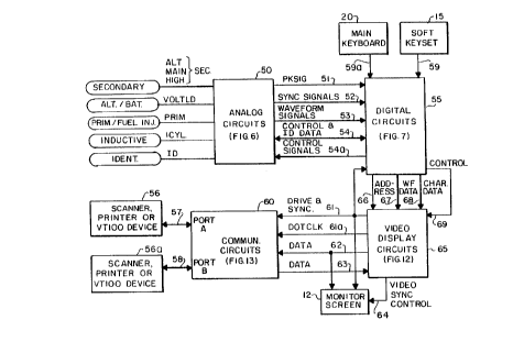
Referring now also to FIG. 4, the signals acquired by
the several leads are applied to analog circuits 50. More
specifically, there is input to the analog circuits 50 a
signal lCYL from the inductive pickup lead 31, a signal PRIM
from the primary/fuel injection lead 33, a signal VOLTLD
from the alternator/battery lead 34 and one or more of three
secondary signals, respectively labeled ALTSEC, MAINSEC and
HIGHSEC, from the secondary lead 32, depending upon the type
of engine being analyzed and the type of pickup coupled to
the inductive lead. In this regard, the secondary lead 32
is preferably a multi-conductor cable which connects to a
multi-conductor pickup device, three of the conductors
serving to provide a three-bit digital ID signal indicating
to the analog circuits 50 an identification of the specific
pickup being used and, thereby, an indication of the type of
ignition system being analyzed. While not illustrated in
FIG. 4, it will be appreciated that the auxiliary lead 36,
when used, can also be coupled to multiple probe or pickup
devices, and it is a multi-conductor cable which will
similarly provide signals identifying the particular probe
or pic~up device used.
The analog circuits 50 are connected by a number of
lines and buses to digital circuits 55. In particular, a
PKSIG signal is applied to the digital circuits 55 via a
conductor 51, a number of sync signals are applied thereto
over line 52 and waveform signals are applied over line 53.
Control and ID data is transferred between the analog
circuits 50 and the digital circuits 55 via bidirectional
bus 54, and control signals are sent from the digital
circuits 55 to the analog circuits 50 via line 54a. The
signals from the soft key set 15 and the main keyboard 20
are also applied to the digital circuits 55 via lines 59 and
59a, respectively.
The engine analyzer 10 also includes communication
circuits 60 havinq ports ~ and B to which peripheral devices
CA 02239912 1998-07-28
56 and 56a may be coupled by bidirectional lines 57 and 58,
respectively. Each of the peripheral devices 56 and 56a may
be a scanner, a printer or other device using the VT100
communication protocol. A scanner is a hand-held device
adapted to be coupled to a computer on-board a vehicle under
test for accessing and reading out the data being monitored
or collected by the on-board computer.
The communication circuits 60 are connected by line 61,
and 61a and data buses 62 and 63 to video display circuits
65, the latter also being connected by a line 64 to the
screen monitor 12 and by the line 61 and by buses 66 and 67
and lines 68 and 69 to the digital circuits 55. More speci-
fically, the line 61 carries drive and sync signals from the
video display circuits 65 to the digital circuits S5, to the
monitor screen 12 and to the communication circuits 60. The
line 61a carries a DOTCLK signal to the communication cir-
cuits 60. The bus 62 carries data from the video display
circuits 65 to the communication circuits 60 and to the
monitor screen 12. The line 64 carries video sync control
signals to the monitor screen 12. The bus 63 carries data
from the communication circuits 60 to the video display
circuits 65. The buses 66 and 67, respectively, carry
address information and waveform data, while the lines 68
and 69, respectively, carry character data and control
signals from the digital circuits 55 to the video display
circuits 65.
O~eratin~ Modes and Features
Before considering the electronic circuits of the
engine analyzer 10 in greater detail, it will be helpful to
briefly describe the user interface with the engine analyzer
10 as regards the above-listed operating modes and features.
In this regard, the system software produces a number of
screen displays on the monitor screen 12, which not only
display test information, but also serve to guide the user
through the operation of the analyzer 10. The major ones of
these screen displays are outlined in FIGS. 26A and 26B.
CA 02239912 1998-07-28
The Primary Menu, the Memory Menu and the Help menu are
not pertinent to the present invention, but will be briefly
described. The Primary Menu permits the user to access
three test options, viz., a Primary Waveform screen which
permits display of a primary waveform, a Dwell Bar graph
screen which measures the closure time of the contact points
in a breaker point ignition system or of an internal switch
in an electronic ignition, and a Duty Cycle Bar Graph screen
which permits display and measurement of fuel system duty
cycle/dwell/voltage signals. The Memory Menu permits the
screen display to be saved in memory and later recalled.
The Help menu permits access to various help instructions
for user assistance in operating various features of the
system. As will be explained below, specific help
instructions can also be accessed from individual test
screen displays. The following screen displays are
pertinent to the present invention:
(a) Start-up (FIG. 17)
(b) Secondary Menu (FIG. 18)
(c) Secondary Waveform (FIG. 19)
(d) Burn Time Bar Graph (FIG. 20)
(e) KV Histograph (FIG. 21)
(f) Cylinder Test Menu (FIG. 22)
(g) Cylinder Time Balance (FIG. 23)
(h) Option Menu (FIG. 24)
(i) Scope Setup (FIG. 25)
Start-u~
Upon powering up the engine analyzer 10, the user first
sets the AC/DC switch 28 (FIG. 5) to the appropriate
position, connects the analyzer 10 to the appropriate power
source and actuates an ON/OFF switch (not shown). This will
cause the start-up display of FIG. 17 to appear on the
monitor screen 12. This screen permits the display of
certain information regarding the engine under test,
including the number of cylinders at 70, the number of
cycles at 71 and the firing order of the cylinders at 72.
CA 02239912 1998-07-28
.
The screen may also display a company logo or other
identifying information at 73. An instructional message
appears at 74, instructing the user to press one of the menu
keys 25 (FIG. 1) or one of the soft keys F1-F6, labels for
which respectively appear on the screen at 74a and 74b as
"Modify Engine Data" and "Help". If the engine analyzer 10
has previously been used for testing a particular engine,
the data for that engine will reappear at 70-72. If the
user now wishes to test a different engine, he presses the
"Modify Engine Data" soft key Fl which will call up the
first of three screens (not shown) to permit the user to
enter the appropriate data. More specifically, the first
screen will instruct him to enter the number of cylinders.
After that is entered, the second screen will automatically
appear which will instruct him to enter the number of
cycles, and finally a screen will appear instructing him to
enter the firing order.
All this information is entered utilizing the numerical
keypad 21 (see FIGS. 1 and lA). Since there are only ten
num~ered keys, on the first of these engine information
screens, the soft keys Fl-F6 will respectively be labeled
11-16 to permit the entry of a number of cylinders greater
than ten. The cursor will automatically appear at the
appropriate place for entry of the appropriate data and, as
each number is entered, the cursor will automatically move
to the position for the next entry. The directional keys 22
may be utilized to move the cursor for the purpose of
correcting mistakes. Once the desired information has been
keyed in, it is entered by pressing the ENTER key 24.
After the firing order information has been entered,
the system will automatically return to the start-up display
of FIG. 17. The user can then move to the desired test
operation by pressing the appropriate one of the ~enu ~eys
25 (FIGS. 1 and lA). If the user is unsure as to how to
proceed during any part of the operation, he can press the
HELP key 26a to brinq up a help display to obtain
assistance.
CA 02239912 1998-07-28
Secondary Menu
If the SECONDARY MENU key 25 is pressed, the screen
display of FIG. 18 will appear. This screen includes a
title at 75 and an instructional messac~e at 76. For this
particular menu there are five options, which are selected
by means of the soft keys Fl-F4 and F6, the labels for which
are respectively displayed at 76a-76e as "Burn Time Bar
Graph", "KV Bar Graph", "KV Histograph", "Secondary
Waveform" and "Return to Start".
Actuation of the "KV Bar Graph" soft key F2 selects a
screen display of a bar graph indicating the live or most
recent cylinder firing voltage for each cylinder, and is not
pertinent to the present invention.
The actuation of the "Return to Start" soft key F6 will
recall the start-up screen display of FIG. 17.
Secondary Waveform
If the "Secondary Waveform" option is selected, the
display at FIG. 19 will appear. This display includes a
title at 77, an indication of the engine rpm at 78 and the
peak voltage reading of the secondary waveform in kilovolts
at 79. The secondary waveform itself, which is the signal
provided by the secondary lead 32, is displayed at 80. In
FIG. 19 there is lllustrated a secondary waveform pattern
for a single cylinder. The number of the cylinder displayed
is highlighted at 78a. This waveform pattern has a
characteristic shape w~ich includes: a high-amplitude spike
80a of very short rise and fall times at the beginning of
the cylinder power stroke, caused by the buildup of voltage
across the spark plug just prior to its firing; a plateau
region 80b of medium amplitude which is the "burn time" when
the spark plug is actually firing; a drop-off portion 80c
when the firing voltage being applied by the coil secondary
is removed from the spark plug; and an oscillatory or
"ringing" portion 80d. (The primary waveform pattern has a
similar characteristic shape.) Labels for the soft keys F1-
F6 are respectively shown at 81a-81f as "Grid On/Off",
"Cursors On/Off", "Waveform Size Select", "Waveform
CA 02239912 1998-07-28
.
Position", "Single/Parade", and "True/Wasted".
The "Grid On/Off" soft key F1 controls selection of the
display of an internally-generated graticule for the
waveform 80. The "Cursors On/Off" soft key F2 controls
selection of the display of horizontal and vertical cursor
lines. The "Waveform Size Select" soft key F3 allows the
left and right directional keys 22 to be used to increase or
decrease the size of the waveform being displayed. The
"Waveform Position" soft key F4 calls up a display for
operator selection of the positioning of the waveform
pattern on the screen. The "Single/Parade" soft key F5
calls up a screen display for operator selection of either a
single waveform pattern for a single cylinder, as
illustrated in FIG. 19, or a parade display of the patterns
for all of the cylinders.
The "True/Wasted" option will appear only in the case
of connection to a distributorless ignition (DI). In that
case, there is typically a coil for every two cylinders,
with each coil firing twice for a single engine cycle.
Thus, every spark plug is fired twice, once in the
compression stroke and once in the exhaust stroke, with the
former being a "true" firing and the latter being a "wasted"
firing. The display of either one can be selected by use of
the screen called up by the soft key F6.
It will be noted that in FIG. 19 all six of the soft
keys F1-F6 are used. If more than six such options are
desired, the excess selections will be displayed on a
separate display screen or "page". In this case, the soft
key F6 on the first display page will be labeled "Next
Page", for selecting the next page, and the soft key F6 on
the second page will be labeled "Previous Page" for
returning to the first page.
Burn Time 8ar Graph
Pressing the "Burn Time Bar Graph" soft ~ey F1 of FIG.
18 will call up the display of FIG. 20 for showing the burn
time for each cylinder, wherein the burn time is the length
CA 02239912 1998-07-28
of time that a spark is arcing being the electrodes of a
spar~ plug. This screen display includes a title 82 and the
engine rpm at 83. The cylinders are listed in a column at
84 in the firing order. Burn time values in milliseconds
are listed in three columns, with minimum values listed at
85, maximum values at 86 and "live" or most recent values at
87. The "line" values are also illustrated in horizontal
bar graph form at 88. Labels for the soft keys F1-F3,
respectively, appear at 89a-89c as "Clear", "Range Select"
and "True/Wasted".
The "Clear" soft key F1 is utilized to clear data from
the screen and to start acquiring fresh data. The "Range
Select" soft key F2 calls up a display for user-selection of
the number of screen divisions per unit of burn time. The
"True/Wasted" label for soft key F3 appears only in the case
of connection to a DI engine and serves the same purpose as
was explained above with respect to FIG. 19.
Burn time bar graph information can be used to
determine the condition of secondary ignition components.
If the burn time for a single cylinder is much shorter or
longer than those for the remaining cylinders, there may be
a problem in relation to the firing of that particular
cylinder. A fouled spark plug, for example, will typically
fire at a lower peak voltage value and sustain a longer burn
time. This may not always show up in the KV bar graph or
histograph. For example, a fouled plug on GM's HEI ignition
system shows up with an acceptable peak voltage value, but
not an acceptable burn time. In this case, the problem is
not so evident on KV test displays, but stands out well on
the Burn Time Bar Graph display of FIG. 20.
KV HistoqraPh
If the "KV Histograph" soft key F3 on the "Secondary
Menu" screen of FIG. 18 is actuated, it calls up the screen
display of FIG. 21. This display includes a title at 90,
and the engine rpm at 91. The cylinder numbers are
displayed at 92, with the cylinder under test ~eing
CA 02239912 1998-07-28
19
highlighted, as by inverse video display. The histograph
pattern itself is displayed at 93 and comprises a graph of
the peak voltage, in kilovolts, required to fire a selected
cylinder over a plurality of successive engine cycles. The
KV value for each firing is displayed at two consecutive
raster locations on the screen to provide some visible width
to that firing display, as indicated at 94. Thus, in a
standard oscilloscope screen, 256 consecutive firings of the
cylinder can be displayed simultaneously. The display
begins to chart the most recent firing voltages on the right
side of the screen and scrolls them to the left, with the
"oldest" firings moving off the left side of the screen.
The speed at which the display scrolls is proportional to
engine speed.
The soft keys F1-F3 are respectively labeled at 95a-95c
as "Clear", "Range Select" and "Cylinder Scan". The "Clear"
soft key F1 is used to clear data from the screen. The
"Range Select" soft key F2 is used for user selection of the
vertical scale of voltage units per screen unit. The
"Cylinder Scan" soft key F3 causes the system to
automatically display one cvlinder for five seconds, and
then automatically move to the next cylinder and on through
the firing order. Pressing this key again turns off the
scan feature and returns to display of the preselected
cylinder values. The cylinder is selected by use of the
numerical keypad 21. If a DI engine is under test, an
additional soft key will be labeled "True/Wasted", as
described above with respect to FIG. 20.
The KV histograph display gives information with
respect to the actual firing voltage required, by
observation of the overall position of the histograph on the
screen with regard to the range scale selected. Chanqes in
the firing voltage are detected by observation of variations
between the individual firing values displayed. Occasional
highs or lows in the firing voltages may indicate an
intermittent problem in the cylinder under test.
CA 02239912 1998-07-28
Cylinder Test Menu
If the CYLINDER TEST MENU key 25 is actuated, it calls
up the screen display of FIG. 22. This display includes a
title at 96 and an instructional message at 97. This
particular menu includes five options, selected by soft keys
Fl-F4 and F6, which are respectively labeled at 98a-98e as
"Cranking Amps Bar Graph", "Cylinder Shorting Bar Graph",
"Cylinder Time Balance Bar Graph", "Vacuum Waveform" and
"Return to Start". The "Cranking Amps Bar Graph", "Cylinder
Shorting Bar Graph" and "Vacuum WaYeform" test features are
not pertinent to the present invention and will not be
further described. The "Return to Start" soft key F6 serves
the same function as was explained above in connection with
FIG. 18.
CYlinder Time Balance
Actuation of the "Cylinder Time Balance Bar Graph" soft
key F3 calls up the screen display of FIG. 23. This display
includes a title at 99 and the engine rpm at 100. This
screen display illustrates a comparison of the cylinder time
periods for each of the several cylinders, wherein the
cylinder time period for a particular cylinder is the time
period from the application of the firing voltage to that
cylinder to the application of the firing voltage to the
next cylinder. Variations in the cylinder time periods from
cylinder to cylinder can give an indication of the relative
power contributions of the cylinders. The overall average
of the cylinder time periods for all of the cylinders is
shown at lOOa. The cylinder numbers are listed in a column
at 101 and opposite each cylinder number is shown its
cylinder time period in milliseconds, at 102. The
percentage differences between the cylinder time period for
each cylinder and the overall average of all the cylinders
is listed at 103 and is graphically shown in a bar graph at
104, wherein the vertical base line is the overall average
of all of the cylinders, and individual cylinder time
periods excPeding that average extend to the right of the
CA 02239912 1998-07-28
base line and those less than the average extend to the left
of the base line.
While it would be possible to display at 102 the actual
latest value of the cylinder time period for each cylinder,
this could result in sufficiently rapid changes in the
display values to be annoying to the viewer. Accordingly,
as will be explained in greater detail below, each of the
cylinder time period values listed at 102 and graphed at 104
is actually an average of the cylinder time periods for the
last ten firings of that cylinder, and the overall average
at 100a i5 the overall average of the cylinder averages
listed at 102.
The soft keys F1 and F2 are respectively labeled at
105a and 105b as "Clear" and "Range S~lect". Selection of
the "Clear" soft key F1 simply clears data from the screen
and begins a new accumulation of data. Actuation of the
"Range Select" soft key F2 changes the scale of the units of
percentage difference in cylinder time period per screen
division unit.
The cylinder time balance information is useful, since
it permits a convenient means of determining the relative
power contributions of the cylinders without having to short
a cylinder, which can be harmful in some newer engines.
O~tion Menu
Pressing the OPTION MENU key 25 calls up the screen
display of FIG. 24. -This display includes a title at 106
and an instructional message at 106a which directs the user
to select among five options by the use of the soft keys F1-
F4 and F6. The soft keys F2, F3 and F6 are, respectively,
labeled at 107b, 107c and 107e as "Scope setup", "Self
Diagnostics", and "Return to Start". The soft key F1 may
have no label or may be labeled "Scanner Port A" or "VT100
Port A", as at 107a, and the soft key F4 may have no label
or may be labeled "Scanner Port B" or "VT100 Port B", as at _~
107d, depending upon what is selected in the Scope Setup
proc~dure, described below. The "Self Diagnostics" feature
10~c is not pertinent to the present invention. The "Return
CA 02239912 1998-07-28
to Start" soft key serves the same function as was explained
above in connection with ~IG. 22.
Actuation of the "Scope Setup" soft key F2 calls up the
screen display of Fig. 25, which is utilized for user
selection of certain operating conditions. The screen
display includes a title at 108 and permits selection among
five types of operating conditions by use of the soft keys
Fl-F5, which are respectively labeled at 108a-108e,
respectively, as 'ISet Time and Date", "Beeper On/Off", "ERR
Message On/Off", "Comm Port Setup" and "Indicators On/Off".
The screen also includes instructional messages 109a-109e
which, respectively, correspond to the soft key selections
and explain for each selection how to effect the change of
operating condition for that selection. The "Set Time and
Date" (108a), the "Beeper On/Off" (108b), the "ERR Message
On/Off" (108c) and the "Indicators On/Off" (108e) selections
are not pertinent to the present invention. If the "Comm
Port Setup" (108d) selection is made, the user can select
the type of device, if any, which is connected to each of
the ports A and B. The up and down directional keys 22 are
used to move the cursor between the port A and port B
messages, and the SELECT key 23 is used to scan among the
several possible device options. Each time the SELECT key
is pressed, the system will scan to the next option which
will then appear next to the corresponding port designation.
The options include a printer, any one of three different
scanners, another device using the VT100 communications
protocol, or no device at all, in which case "OFF" will
appear on the screen for that port.
Where a VTlOO device is selected, the label for the
corresponding soft key (e.g., F1) on the option menu screen
(FIG. 24) will be "Scanner Port A" or "VT100 Port A",
respectively. If a printer or no device is selected, the
corresponding soft key Fl or F4 on the option menu screen
display of FIG. 24 will have no label. If a scanner or
VT100 device is selected, actuation of the corresponding
soft key (F1 or F4) on the option menu screen display of
CA 02239912 1998-07-28
FIG. 24 will activate a suitable program sub-routine which
is designed to interface with a corresponding device type
and will call up a screen display tnot shown) for that
device type. More specifically, as will be explained in
greater detail below, the selected screen display will have
soft key labels corresponding to function keys on the device
and the program will permit those device functions to be
actuated by operation of the soft keys F1-F6 of the engine
analyzer 10.
Analo~ Circuits
The basic function of the analog circuits 50 tsee FIG.
4) is to provide an interface between the lead set 30 and
the remaining circuitry of the engine analyzer 10. It
receives the analog input signals frcm the lead set and
places them in proper condition for handling by the digital
circuits 5S. Referring to FIG. 6 the secondary signals
ALTSEC, MAINSEC and HIGHSEC from the secondary lead 32 are
applied to conditioning circuitry llo, which preferably
includes three separate channels of circuitry for
respectively adjusting the levels of the three different
secondary signals to provide an adequate size display on the
monitor screen 12, and buffering to provide isolation
between the engine analyzer 10 and external devices. Which
of the three different secondary signals is present will
depend upon the type of pickup device coupled to the
secondary lead which-will, in turn, depend on the type of
ignition system under test.
Normally, there will be only one secondary signal,
typically MAINSEC, but in the case of a DI engine there will
be two secondary signals present, typically ALTSEC and
MAINSEC. From the conditioning circuitry 110, the ALTSEC
and MAINSEC signals are applled to absolute value amplifiers
lll, which simply detect the magnitude of the voltage
signals, which may be either positive-going or negative-
going, and output them as posltive-going signals. These
amplifiers are required only for DI inputs. The ALTSEC and
MAINSEC signals are also
CA 02239912 1998-07-28
24
applied to conditioning circuitry 112, which produces the
signals DISYNC and DIPOL. The conditioned ALTSEC and
MAINSEC signals from the conditioning circuitry 110 are also
applied to an electronic switch 113 which selects between
the two inputs in response to a control signal SWA, and
outputs the selected signal to an electronic signal select
switch 114. The conditioned MAINSEC and HIGHSEC signals
from the conditioning circuitry 110 are also applied
directly to the switch 114, as well as to an electronic
switch 115.
The VOLTLD signal from the alternator/battery lead 34
is applied through conditioning circuitry 116 which outputs
the signal AUXB to the switches 114 and 11~. The PRIM
signal from the primary/fuel injection lead 23 is applied to
conditioning circuitry 117, which produces an output signal
PRI which is applied directly to the switch 114. The PRI
signal is also further conditioned in conditioning circuitry
118, the output of which is applied to the switch 115. Also
input to the switch 115 is a SELSIG signal, the source of
which will be explained below. The switch 114 is a signal
select switch which effectively selects which one of the
several input signals is to be displayed on the monitor
screen 12, under the control of a switching signal SWB. The
switch 115 is a sync select switch which, under the control
of a signal SWC, selects which of the incoming signals is to
be used as the sync~source.
The selected output of the switch 114 is applied
directly to one input of an electronic switch 120, and is
applied through an inverter 121 to a second input of the
switch 120, which selects the inverted or non-inverted
signal under the control of a signal SWD, the selected
signal being amplified in an amplifier 122 to produce a KVIN
analog wavefor~ signal. The KVIN signal is compared to a
threshold voltage level in a comparator 123, which outputs a
BRNT signal to an electronic switch 124. The KVIN signal is
also applied directly to another input of the switch 124 to
CA 02239912 1998-07-28
an input of an electronic switch 125, the other inputs of
which receive the output signals from the absolute value
amplifiers 111. T~e switch 125 operates under the control
of a signal SWE to pass the two secondary signal inputs from
the absolute value amplifiers 111, in the case of a DI
engine, and apply them respectively to peak hold circuits
126 and 127. Otherwise, the switch 125 directs the KVIN
signal to the peak hold circuit 127.
The peak hold circuits 126 and 127 are of conventional
construction and capture the maximum or peak amplitude
values of the input analog signals, which peak values are
respectively fed to the two inputs of an electronic switch
128, which operates under the control of a signal SWF to
select one of these inputs to produce an output signal KVOUT
which is applied to another input of the switch 124. The
KVIN signal is also applied directly to the switch 124. The
switch 124 has three outputs and operates under the control
of a signal SWG to switch the KVOUT signal to one output 51
as a PKSIG signal, which is sent to the digital circuits S5.
The BRNT signal is switched to a second output as a LABSYNC
signal, which is also directed to the digital circuits 55.
The KVIN signal is directed to the third output as the
SELSIG signal which, as was explained above, is directed to
an input of the switch 115 to use the displayed signal as
the sync source.
The KVIN signal-~is also applied to a summing amplifier
129 which produces a waveform output signal VIN, which is
sent to the digital circuits 55 over the line 53.
The sync source selected ~y the switch 115 is applied
to a comparator 130, which compares it to a reference level.
This reference level is variable and is proportional to the
width of a control signal PWM received from the digital cir-
cuits 55 via the line 54a, and which is applied to the reset
terminal of a flip-flop 131, which produces at its -Q output
a pulse having a width proportional to the width of the PWM
signal and which is converted to a DC voltage level in an
CA 02239912 1998-07-28
amplifier 131a to provide the threshold reference level for
the comparator 130. The comparator 130 outputs a pulse
signal on line 13Oa which is high whenever the output of the
switch 115 is above the threshold level. This output is
applied to a blanking circuit 132, which responds each time
the comparator output goes high to blank the signal for a
predetermined time period, so that the output of the
blanking circuit 132 is a pulse signal ENGSYNC, which is
applied to the digital circuits 55.
Basically the ENGSYNC signal is a timing signal which
comprises a short pulse responsive to the spike in primary,
secondary and fuel injection waveforms at the beginning of
each cylinder time period, corresponding in time to the
application of the firing voltage to the spark plug. It is
desired that there be only a single ENGSYNC pulse for each
cylinder. However, the ringing portion of the secondary
wave pattern (see FIG. 19) may sometimes have an amplitude
sufficient to exceed the threshold level in the comparator
130, which would produce a second pulse for that cylinder.
Also, some modern engines intentionally provide multiple
firings of each spark plug during each engine cycle to
promote better combustion of the fuel, and each such firing
will cause an output from the comparator 130. The blanking
circuit 132, which may be of the type disclosed in U.S.
patent no. 4,095,170, ensures that the ENGSYNC signal will
include only the first spark plug firing in each cylinder
time period, and that any other excursions of the waveform
pattern above the threshold of the comparator 130 during
that cylinder time period will be ignored.
The lCYL signal from the inductive pickup lead 31 is
applied through conditioning circuitry 138 which outputs a
lSYNC signal to the digital circuits 55. The three sync
signals LABSYNC, ENGSYNC and lSYNC are all fed to the
digital circuits 55 via the line 52.
The ID signals rom the secondary lead 32 (or the
auxiliary lead 36, T~hen used) are applied in parallel to an
CA 02239912 1998-07-28
.
identification latch 139, to which is also applied the DIPOL
signal. The latch 139 has an eight-bit output which is
applied over the bus 54 to the digital circuits 55. The
latch 139 is controlled by an ANCLKA signal and an -OC4
signal received from the digital circuits 55 (and
specifically from FIG. 8) over the line 54a. The bus 54,
which is bidirectional, also carries switch control data
from the digital circuits 55 to the input of a switch
control latch 142, which is further controlled by an ANCLKB
signal received from the digital circuits 55 over the line
54a to produce the switch control signals SWA-SWG for the
switches 113-115, 120, 124, 125 and 128. The bus 54 also
carries vertical position data from the digital circuits 55
to the input of a D/A converter 141, which outputs an analog
VPOS signal to the summing amplifier 129 to vary the
vertical position of the waveform.
The output of the latch 139 provides identification
signals to the digital circuits 55 so that the latter can
identify the particular pickup being used. In the case of
DI engines, the DIPOL signal indicates the polarity of the
signal to determine whether it is a positive or a negative
firing. Armed with this identification information, the
digital circuits generate ANCLKA and ANCLKB signals for
controlling the latches 139 and 142 and the switch control
data for the latch 142 so it can output the appropriate
switch control signals.
Diqital Circuits
The digital circuits 55 are shown in FIG. 7 and their
basic functions are to read the main keyboard 20 and the
soft key set 15, to control the operations of the analog
circuits 50, and to receive and manipulate data from the
analog circuits 50. The heart of the digital circuits 55 is
a microprocessor 145 which is coupled to the soft key set 15
and to the main keyboard 20. The microprocessor 145 is also
coupled to the analog circuits 50, receiving therefrom the
PKSIG signal on the line ~ he sync signals on the line 52
CA 02239912 1998-07-28
28
and the ID signals on the bus 54. The microprocessor 145
outputs the PWM and -OC4 signals to the analog circuits 50
on the line 54a. The microprocessor 145 is also coupled by
the bidirectional data bus S4 and by an address bus 144 to a
transmitter/receiver 140, an EPROM 146, a non-volatile
character RAM 147, screen delay circuitry 155 and a display
sample cloc~ generator 150. Address signals from the
microprocessor 145 are transmitted through the transmitter/
receiver 140 to the video display circuits 65 via the
address bus 66.
A RAMC signal from the microprocessor 145 is applied to
one input of an AND gate 148, the output of which is applied
to the WE terminal of a non-volatile waveform RAM 149, which
receives waveform data from a waveform sample and store -
circuit 160. That data is also sent to the video display
circuits 65 (FIG. 12) via the data bus 67. Address
information is transmitted from a memory address and control
circuit 180 (FIG. 11) to the waveform RAM 149 and to the
video display circuits 65 via the address bus 66. The
memory address and control circuit 180 also applies a NR
signal to the other input of the AND gate 148, and applies a
FREEZE signal to the waveform sample and store circuit 160.
The microprocessor 145 produces a 4 MHz clock signal
which is applied to the waveform sample and store circuit
160 and to the display sample cloc~ generator 150, the
latter producing a three-phase display sample clock signal
which is applied to the screen delay circuitry 155 and to
the waveform sample and store circuit 160. The display
sample cloc~ generator 150 also generates the ANCLXA and
ANCLXB signals, which are sent to the analog circuits 50 via
the line 54a, and a CLOCX signal, which is sent to the
screen delay circuitry 155. The screen delay circuitry 155
generates a SETOUT signal and an RBLX signal, which are
applied to the memory address and control circuit 180, and a
FIFORD signal which is applied to the waveform sample and
store circuit 160. The waveform sample and store circuit
CA 02239912 1998-07-28
29
160 also receives from the analog circuits 50 the waveform
signals via the line 53 and the ENGSYNC signal, and further
receives from the microprocessor 145 a PEAK signal. The
microprocessor 145 also sends control signals to the
character RAM 147 and a SETUP signal to the display sample
clock generator 150.
The memory address and control circuit 180 receives
from the microprocessor 145 an INT-EX signal, a BLOCK1
signal, a CYLID signal, a SYNC signal and an FRZST signal.
It further receives from the video display clrcuits 65 a
VERTDR signal, and outputs control signals to the video
display circuits 65 on the line 69.
Video display information from the video display
circuits 65 is-applied to the microprocessor 145 as a VIDTXD
signal. As was explained above in connection with FIGS. 17-
25, the screen displays may include not only waveform data
but also alphanumeric or other types of character data.
This latter data is sent to the video display circuits 65
via the data bus 68 as a DIGTXD signal.
The EPROM 146 stores the operating program for the
microprocessor 145. The character RAM 147 is a non-volatile
RAM which receives character data from the microprocessor
145 and stores it at designated addresses. One portion of
the RAM 147 acts as a serial buffer. Periodically data is
transferred from other portions of the RAM 147 into the
serial buffer portion and is read out bac~ to the
microprocessor 145, which then transmits the data serially
in the DIGTXD signal to the video display circuits 65. In
the KV Histograph mode of operation, data is transferred
from the character RAM 147 to the wavefor~ RAM 149, and
thence to the video display circuits 65 via the
transmitter/receiver 140, as will be explained more fully
below.
The display sample cloc~ generator 150 generates a
display sample clock signal which controls the rate at which
samples will be taken frcm the analog input waveform for
CA 02239912 1998-07-28
,-- .
display on the monitor screen 12. The waveform sample and
store circuit 160 effects the actual sampling of the analog
waveform and passes the samples selected for display to the
waveform RAM 149 where they are temporarily stored for
display, before transfer to the video display circuits 65
via the data bus 67. The address signals for the waveform
RAM 149 are generated by the memory address and control
circuit 180.
Dis~lay Sample Clock Generator
The display sample clock generator 150 is shown in FIG.
8 and includes a port expander and counter 151 which is
coupled to the data bus 54 and the address bus 144 and also
receives the 4 MHz clock signal from the microprocessor 145.
The port expander and counter 151 generates the ANCLRA and
ANCLKB signals, and also generates the CLOCK signal, which
is applied to the clock input of a flip-flop 152, as well as
to the screen delay circuitry 155 of FIG. 9. The Q output
of the flip-flop 152 is connected to the lD input of a quad
flip-flop 153 which is clocked by the 4 MHz clock signal.
The quad flip-flop 153 has four Q outputs and four -Q
outputs. The lQ output is connected to the 2D input. The
-lQ output is connected to the clear terminal of the flip-
flop 152. The 2Q output is connected to the 3D input. The
SETUP signal from the microprocessor 145 is connected to the
clear terminal of the quad flip-flop 153.
Screen Delay Circuitry
The screen delay circuitry 155 is illustrated in FIG.
9, and includes a port expander and counter 156 which is
coupled to the data bus 54 and to the address bus 144 for
receiving data and address signals from the microprocessor
145, and also receives the CLOC~ signal from the display
sample clock generator 150 (FIG. ~). The port expander and
counter 156 generates a PEAK signal which is applied to the
waveform sample and store circuits 160 (FIG. 10). It also
generates the CSYNC, BLOCX1, CYLID and RBLK signals -~hich
are applied to the memory address and control circuit 180
CA 02239912 1998-07-28
(FIG. 11). The port expander and counter 156 also generates
a cloc~ signal which it applies to the clock input of a
flip-flop 157, the Q output of which is connected to the D
input of a flip-flop 158, the clock and preset inputs of
which respectively receive the CLKC- and CLKB- signals from
the display sample clock generator (FIG. 8). The Q output
of the flip-flop 157 also constitutes the SETOUT signal,
which is applied to the memory address and control circuit
180 (FIG. 11). The -Q output of the flip-flop 158 is the
FIFORD signal, which is applied t~ the waveform sample and
store circuit 160 (FIG. 10).
Waveform Sample and Store Circuit
The waveform sample and store circuit 160 is shown in
FIG. 10, and includes an ~/D converter 161 which receives
the VREF and VIN signals from the analog circuits 50 (FIG.
6). The VREF signal provides a precise voltage reference
for the A/D converter 161. This reference level is
determined by the microprocessor 14S in the digital circuits
55 (FIG. 7), but the microprocessor 145 does not have the
ability to put out an analog voltage. Therefore, it outputs
a digital byte to the D/A converter 141 (FIG. 6), which
converts that number to an analog voltage level. The A/D
converter 161 receives the 4 MXz clock signal and samples
t~e analog waveform signal VIN at a 4 NHZ rate, outputting
8-bit digital samples on the data bus 162 to a latch 163 and
to the P input of a~magnitude comparator 164. The latch 163
and the Q input of the magnitude comparator 164 are also
interconnected by a data bus 166, which is also coupled to a
first-in-first-out (FIFO) storage circuit 165. The CLKC-
signals from the display sample clock ~enerator 150 (FIG. 8)
are coupled to the clear terminal of the latch 163.
The P greater than Q output of the magnitude comparator
164 is applied to the D input of a flip-flop 167, the Q
output of which is applied to one input of an OR gate 168.
The 4 MHz c~ock signal is applied to the cloc~ input of the
flip-flop 167 and to the other input of the OR gate 168, the
CA 02239912 1998-07-28
output of which is applied to one input of an OR gate 169.
The -Q output of the flip-flop 167 is connected to the clock
input of the latch 163.
The PEAK signal from the screen delay circuitry 155
(FIG. 9) is applied to the D input of a flip-flop 170, the
clock input of which receives the ENGSYNC signal from the
analog circuits 50 (FIG. 6). The Q output of the flip-flop
170 is connected to one input of an OR gate 171, the other
input of which receives the CLKA- signal from the display
sample clock generator 150 (FIG. 8). The output of the OR
gate 171 is connected to the clear terminal of the flip-flop
167 and, through an inverter 172 to the other input of the
OR gate 169, the output of which is connected to the preset
terminal of the flip-flop 167. The Q output of the flip-
flop 170 is also connected to the load input of a counter
175, the count up input of which receives the CLKA signal
from the display sample clock generator 150 (FIG. 8). The
counter 175 has a carry output which is connected to the
clear terminal of the flip-flop 170.
The FIFO storage circuit 165 has a write input W which
receives the CLKA- signal from the display sample clock
generator 150 (FIG. 8), and a read input R which is
connected to the output of an OR gate 177, the inputs of
which receive the FIFORD signal from the screen delay
circuitry 155 (FIG. 9) and the FREEZE signal from the memory
address and control circuit 180 (FIG. 11). The output of
the FIFO storage circuit 165 is applied via the data bus 67
to the waveform RAM 149 (FIG. 7).
Fundamentally, whatever sample value is stored in the
latch 163 is present at the input of the ~IFO storage
circuit 165, and is written thereinto each time a C~XA-
pulse appears, i.e., at the display sample cloc~ rate, which
is a rate set to provide 51Z display samples during each
cylinder period. This rate is much slower than the 4 MHz
ra~e at which the analog waveform signal is being sampled by
the A/D converter 161. But this display sample cloc~ rate
CA 02239912 1998-07-28
is more than adequate to accurately reproduce most portions
of the analog input waveform. Thus, most of the time, most
of the samples from the A/D converter 161 are not needed and
only selected ones of them are displayed. But the waveform
sample and store circuit 160 is continuously operating to
store the maximum sample value which occurs during each
cylinder period. Thus, during high frequency portions of
the waveform which are too rapid to be accurately captured
by the display sample clock rate, the circuitry switches to
select the stored peak values for display.
Memory Address and Control Circuit
The memory address and control circuit 180 is shown in
FIG. 11. It basically operates to generate the display
address signals and certain control signals for waveform RAM
149 and for waveform display by the video display circuits
65, as well as certain control signals for other portions of
the digital circuits 55. A flip-flop 181 receives the CLRA
signal at its clock input and the CLKC- signal at its clear
terminal. The CLKA signal is also connected to the clock
input of an address counter 182, which outputs 9-bit digital
address signals on the data bus 66 to the waveform RAM 149
and the video display circuits 65 (FIG. 12). The address
counter 182 also has an overflow output which is connected
to the clock input of a flip-flop 184, the Q output of which
is connected to the count input of the address counter 182
and to one input of an AND gate 185, the other input of
which receives the CLXC signal from the display sample cloc~
generator 150 (FIG. 8). The output of the AND gate 185 is
connected to one input of an AND gate 186, the other input
of which receives the INT-EX signal from the microprocessor
145 (FIG. 7). The output of the AND gate 186 is applied to
the clock input of the flip-flop 187, the preset terminal of
which receives the SYNC signal from the microprocessor 145
(FIG. 7~. The Q output of the flip-flop 187 is connected to
the D input of the flip-flop 181 and to one input of an OR
gate 189, the other input of which is connected to the
CA 02239912 1998-07-28
34
overflow output of the address counter 182. The -Q output
of the flip-flop 181 is connected to the clear terminal of
the flip-flop 187 and to one input of an AND gate 188, the
output of which is connected to the clear terminal of the
flip-flop 184.
The output of the OR gate 189 is connected to the count
up input of a cylinder counter 190 and to one input of an
AND gate 191, the other input of which receives the CSYNC
signal from the screen delay circuitry 155 (FIG. 9), and the
output of which is connected to the clear terminal of the
cylinder counter 190. The load terminal of the cylinder
counter 190 is connected to the output of an OR gate 192,
one input of which receives the BLOCKl signal from the
screen delay circuitry 155 (FIG. 9), and the other input of
which is connected to the A=B output of a comparator 195.
The 4-bit A input of the comparator 195 is connected to the
output of the cylinder counter 190, which is also coupled to
the address bus 66, while the 4-bit B input of the
comparator 195 receives the CYLID signal from the screen
delay circuitry 155 (FIG. 9). The cylinder counter 190 also
receives a 4-bit RBLK signal from the screen delay circuitry
155 (FIG. 9).
The A=B output of the comparator 195 is also connected
to the clock input of a flip-flop 196 and, through an
inverter 197, to the clock inputs of flip-flops 198 and 199.
The -Q output of the-flip-flop 198 is connected to the other
input of the AND gate 188. The D input of the flip-flop 198
receives the FRZST signal from the microprocessor 145 (FIG.
7). The -Q output of the flip-flop 199 is connected to one
input of an OR gate 200, the other input of which receives
the VERTDR signal from the video display circuits 65 (FIG.
12). The output of the OR gate 200 is connected to the
clear terminals of the flip-flops 196 and 199 and to the
clock input of a flip-flop 201. The Q and -Q terminals of
the flip-flop 201 respectively output signals MA and MB
which are sent via the line 69 to the video display circuits
CA 02239912 1998-07-28
65 (FIG. 12). The MB signal is also connected to the D
input of the flip-flop 201.
The -Q output of the flip-flop 196 and the Q output of
the flip-flop 199 are respectively connected to the two
inputs of an OR gate 202, the output of which is connected
to one input of an OR gate 203. An OR gate 204 has the two
inputs thereof respectively connected to receive the CLXB-
signal from the display sample clock generator 150 (FIG. 8)
and the SETOUT signal from the screen delay circuitry 155
(FIG. 9). The output of the OR gate 204 is connected to one
input of an OR gate 205, the other input of which is
connected to the Q output of the flip-flop 184. The output
of the OR gate 205 is a signal MEMWRA, which is applied to
the other input of the OR gate 203 and to one input of an OR
gate 206, the other input of which is a FREEZE signal which
is received from the Q output of the flip-flop 198. The
output of the OR gate 203 is a MEMWRB signal, which is sent
via the line 69 to the video display circuits 65 (FIG. 12).
The output of the OR gate 206 is the WR signal which is sent
to the gate 148 on FIG. 7. The FREEZE signal is also sent
to the waveform sample and store circuit 160 (FIG. 10).
Video Display Circuits
The video display circuits 65, illustrated in FIG. 12,
generate and control the screen displays on the monitor
screen 12. The circuits include a microprocessor 210 and an
electronically programmable logic device (EPLD) 211 which
cooperate to control the operation of the video display
circuits 65. A clock oscillator 212 provides a master clock
signal DOTCLX which is applied to the EPLD 211 and to the
communication circuits (FIG. 13) via the line 61a. The E~LD
211 is programmed by PROGRAM signals from the microprocessor
210 to generate screen address signals which are sent via a
data bus 216 to a waveform display RAM 214. The program for
operating the microprocessor 210 is stored in a program ROM
213.
i
CA 02239912 l998-07-28
36
Waveform data is fed to the RAM 214 from the digital
circuits 55 (FIG. 7) via the data bus 67 and is written into
the RAM at addresses designated by address information
received from the memory address and control circuits 180
(FIGS. 7 and 11) via the bus 66. The waveform data is read
out of the RAM 214 to a fill-in-the-dots circuit 215 which
generates data to fill in the spaces between waveform
samples on the display screen. This circuit may be of the
type disclosed in the aforementioned U.S. patent no.
4,800,378. The waveform data is read from the RAM 214 at
addresses controlled by the screen address data which is
received from the EPLD 211 on the bus 216.
The RAM 214 is a dual port RAM, which is essentially
divided into two portions, with the input data being written
alternately into the two portions, so that one portion can
be read from while the other is being written to. The RAM
214 is enabled by the MEMWRB signal and the switching
between the portions is controlled by the MA and MB signals,
all received on the line 69 from the memory address and
control circuit 180 (FIGS. 7 and 11). The waveform data
from the fill-in-the-dots circuit 215 is read serially into
the EPLD 211 for transfer to the monitor screen 12 and to
the communication circuits 60 (FIG. 13) in the VII:EO signal
on line 62.
Character data can be received either from the digital
circuits 55 (FIG. 7)- in the DIGTXD signal on line 68, being
then transferred to the microprocessor 210 in the ~ IN
signal, or from the communication circuits 60 (FIG. 13) in
the COMTXD signal on line 63, which is also input to the
microprocessor 210. Character data may also be obtained
from a screen ROM 217 which stores format information for
the various screen displays, such as titles, headings,
instructional text and the like, this information being read
by the microprocessor 210. Information is read from the
ROMS 213 and 217 under the control of address signals from
the microprocessor 210 via a bus 220, the data being -ead
:
CA 02239912 1998-07-28
out on the bus 221.
The microprocessor 210 determines where the character
information is to be displayed on the screen and the
attributes with which it is to be displayed, such as whether
it is to be in inverse video, flashing, single or double
height or width, and the intensity and color of its display,
as well as whether it is to override waveform data appearing
at the same screen location. The character data is fed to a
character RAM 218 and the attribute data is fed to an
attribute RAM 219 over the data b~s 221, to be written into
those RAMS at addresses determined by address information on
the bus 220. The character and attribute information is
read from the RAMs 218 and 219 for display at screen
addresses determined by address data generated by the EPLD
211 on a bus 222. The attribute data is sent directly to
the EPLD 211 on a bus 223, while the character data is sent
via a bus 224 to a character generator 225, which assembles
the bit pattern for each character and transmits the
information serially to the EPLD 211. The EPLD 211
determines whether or not the character data, at any screen
location, is to override waveform data and outputs the
character and attribute data to the monitor or to the
communication circuits 60 (FIG. 13) in the VIDEO signal.
The EPLD 211 also generates the video sync control
signals which are applied to the monitor screen 12 via the
line 64. The microprocessor 210 generates a VIDTXD signal
which contains video data which is transmitted to the
digital circuits 55 (FIG. 7) and to the communication
circuits 60 (FIG. 13) on the line 61.
Communicatlon Circuits
The communication circuits 60 are shown in FIG. 13 and
operate to provide an interface between peripheral devices,
such as a scanner or a printer, and the monitor 12, the
digital circuits 55 and the video display circuits 65. The
communication circuits 60 include a microprocessor 230,
-~hich is coupled to the ports A and B by a transmitter/
CA 02239912 1998-07-28
38
receiver 231, which is essentially a level translator. The
program for the microprocessor 230 is stored in an EPROM 232
which is addressed by the microprocessor 230 via a bus 233,
the program data being sent to the microprocessor 230 over a
data bus 234.
The VIDEO screen data from the video display circuits
65 (FIG. 12) are stored in a RAM 235, being written
thereinto at addresses generated by an address counter 236,
which receives control LD and TRIG signals from the
microprocessor 230. The TRIG signal is also applied to
control logic 237, which also receives the ~OTCLX signal
from the video display circuits 65 (FIG. 12) via the line
61a and generates BDOT signals for controlling the clock
rate of the address counter 236 and the RAM 235. Data to be
printed is read out from the RAM 235 to the microprocessor
230 over a line 238 under the control of address signals
generated by the microprocessor 230 and applied to the RAM
235 through a latch 239. The microprocessor 230 also
receives the VERTDR signal and the VIDTXD signal from the
video display circuits 65 (FIG. 12) on line 61 and outputs a
COMTXD signal on the line 63 to the video display circuits
65.
Operation
Assuming that the analyzer 10 (FIG. 1) has not
previously been used, upon power up the start-up display of
FIG. 17 will appear on the monitor screen 12. The first
thing that the user must do is enter information regarding
the engine to be tested, which he does by pressing the soft
key F1 to call up the data entry screens as explained a~ove.
The user can then, by pressing the OPTION MENU key 25, call
up the option menu screen display of FIG. 24, which permits
him to access the Scope Setup screen display of FIG. 25,
which permits him to program in information concerning what
type of equipment, if any, is connected to each of the ports
A and B (FIG. 4).
CA 02239912 1998-07-28
The microprocessor 145 in the digital circuits 55 (FIG.
7) monitors the key strokes used to enter all of this
information, and stores the information in the non-volatile
character ~AM 147. The information is also transferred in
the DIGTXD signal over line 68 to the EPLD 211 and thence to
the microprocessor 210 in the video display circuits 65
(FIG. 12), and thence in the VIDTXD signal on line 61 to the
microprocessor 230 in the communication circuits 60 (FIG.
13). Each of the microprocessors 210 and 230 has sufficient
internal RAM to store this setup information. This
information will be used ~y all of the microprocessors to
tailor each of the display screens to the particular type of
engine being tested, and to tailor the scanner interface
mode of operation to the particular type of scanner
connected. Because the character RAM 147 is non-volatile,
it will retain all of the setup information when the
analyzer 10 is powered down. Thus, when it is again powered
up, the microprocessor 145 will reinitialize itself in
accordance with the saved setup information, and will
accordingly initialize the microprocessors 210 and 230.
All waveform data is obtained from the lead set 30,
processed in the analog circuits 50, digitized in the
digital circuits 55 and arranged in the video display
circuits 65 for display on the monitor screen 12. The
particular waveform display and the for~at of the display
are determined by the user via selections made with the soft
key set 15 and the main keyboard 20. In the illustrated
embodiment, any one of five different waveform inputs might
be displayed, viz., the VOLTLD signal from the alternator/
battery lead 34, the PRIM signal from the primarylfuel
injection lead 33, and any one of the three possible
secondary signals ALTSEC, MAINSEC and HIGHSEC from the
secondary lead 32. Each of these signals is applied, after
conditioning, to the signal select switch 114 and to the
sync select switch 115. It will be appreciated that, if
desired, additional waveform si~nals could also be detected
;
CA 022399l2 l998-07-28
and applied to the switches 114 and 115. For example,
pickups or probes could be connected to the auxiliary lead
36 to provide associated input signals (not shown). The
switch 114 selects the input signal to be displayed on the
screen, while the switch 115 selects the signal which is to
serve as the sync source.
Thus, it will be appreciated that the engine analyzer
10 permits the display of one signal while syncing off
another signal. The microprocessor 145 in the digital
circuits 55 is programmed so that, as it goes into each
waveform mode of operation, it selects the appropriate sync
source to operate from. Sometimes this is variable. For
example, if a secondary signal is being displayed, it would
normally be preferable to work with a secondary sync signal.
However, if the microprocessor determines that the secondary
sync signal is not stable, or is completely missing, it can
switch over to the primary sync signal. But on some newer
cars a primary sync signal is not accessible, in which case
the microprocessor would switch back to the secondary sync
signal.
The engine analyzer 10 is also capable of operation in
a labscope mode in which the operator can choose among the
labscope input itself, or the primary, secondary or number 1
cylinder signals for use as a sync source or, alternatively
the analyzer 10 can use no sync signal at all and simply run
on a time base.
The switches 113 and 120 are utilized for DI engines,
which require two secondary inputs, viz., ALTSEC and
MAINSEC. In this event, each coil is connected to two
different spark plugs so that each time that the coii
outputs a firing voltage it fires both spark plugs, and it
does this twice during each engine cycle. Thus, for each
firing, one of the plugs being fired is a "true" firing in
the compression stroke, while the other is a "wasted" firing
in the exhaust stroke. Switch 113 is constantly switching
under the control of the signal SWA, which is in _ur~
CA 022399l2 l998-07-28
41
generated under the control of the microprocessor 145, to
select the "true" one of the two secondary inputs.
Furthermore, during each engine cycle, half of the
"true" firings will be positive and half will be negative.
Thus, both inverted and non-inverted forms of the selected
output from the signal select switch 114 are applied to the
switch 120, which is continually switching under the control
of the SWD signal for selecting between the inverted and
non-inverted forms of the waveform, so that the screen
display will always be positive.
The microprocessor 14 5 (FIG. 7) is able to make the
switching decisions because it knows the nature and polarity
of the input waveform signals from the ID and DIPOL signals
applied to the identification latch 139 (FIG. 6).
Furthermore, from this information the microprocessor also
knows to have the sync select switch 115 select the DISYNC
sync source instead of using the normal secondary sync that
would be used for a conventional ignition.
The sync source selected by the switch 115 is applied
to the comparator 130 for generating the ENGSYNC signal.
More specifically, referring to FIG. 14, the analog waveform
signal is illustrated in waveform A, in this case a
secondary voltage pattern 80. That signal is compared in
the comparator 130 with a threshold level 241, the output of
the comparator 130 going high when the analog sync signal
exceeds the threshol~ level 241, and returning low to when
it drops back below the threshold level. The blanking
circuit 13 2 blanks out the output of the comparator 130 a
very short time after it goes high and for the remainder of
the cylinder period to produce a short pulse 242 as the
ENGSYNC signal and to ensure that there will be no further
ENGSYNC pulses during that cylinder period, as was explained
above in connection with FIG. 6A.
Character information to be displayed on the monitor
screen 12 may come from any of a number of sources, viz.:
(a) the lead set 30, which provides voltage level
CA 02239912 1998-07-28
information, such as for the KV histograph, and timing
information, such as for the cylinder time balance and spark
plug burn time analyses; (b) from the main keyboard 20, such
as engine information keyed in by the user; (c) from the
screen ROM 217 (FIG. 12), which provides background formats
for the various screen displays; and (d) from an associated
scanner via the communication circuits 60 (FIG. 13).
In the case of voltage level signals from the lead set
30, the waveform signals are selected by the switch 125 and
applied to the peak hold circuits 126 and 127. For DI
engines there are two input waveforms, which include both
positive and negative polarity signals. Thus, they are both
first passed through the absolute value amplifiers 111 to
provide positive going outputs, and the switch 125 passes
both signals respectively to the peaX hold circuits 126 and
127. The switch 128 selects only one of these peak signals
for display at any given time. In the case of a standard
ignition, the switch 125 selects the KVIN signal from the
switches 114 and 120, and directs it to the peak hold
circuit 127, the output of which is passed by the switch
128. The output of the switch 128 is the KVOUT signal,
which is passed by the switch 124 as the PKSIG signal. The
KVIN signal is also applied directly to the switch 124,
which passes it as the SELSIG signal, which is in turn fed
back to the input of the switch 115 so it is available for
selection as a sync source.
The KVIN signal is also compared in the comparator 123
to a threshold level which, for purposes of illustration
will be assumed to be substantially the same as the level
241 (FIG. 14). When it exceeds this threshold the output of
the comparator 123 goes high to form the BRNT signal, which
is passed by the switch 124 as the LABSYNC pulse signals
243, illustrated in waveform D of FIG. 14, which return low
at 245 when the waveform voltage drops back below the
threshold level 241.
CA 02239912 1998-07-28
The lCYL signal is passed through conditioning
circuitry 138, which includes a fairly low threshold level
which, for convenience, is again assumed to be the same as
the threshold level 241 in FIG. 14. The conditioning
circuitry 138 includes a multivibrator which produces an
output lSYNC signal, illustrated in waveform B of FIG. 14,
which comprises a short pulse 244 each time the firing
voltage is applied to the number 1 cylinder.
All of the information from the analog circuits is
passed to the digital circuits 55 (FIG. 7). The waveform
signals, which include the analog waveform signal VIN and
the reference signal VREF, are applied to the waveform
sample and store circuit 160, which digitizes the VIN signal
for display. This digitizing operation occurs under the
control of display sample clock signals from the display
sample clock generator 150, which control the rate at which
the samples are selected for display, and signals from the
screen delay circuitry 155, which control the horizontal
positioning of the waveform on the screen. The waveform
display samples are stored in the waveform RAM 149 at
addresses determined by an address counter in the memory
address and control circuit 180, for use in the FREEZE
function, described hereinafter. The display samples are
also passed via the data bus 67 to the waveform display RAM
214 of the video display circuits 65 (FIG. 12), where they
are stored at addresses generated by the memory address and
control circuit 180 and passed over the address bus 66.
Referring to FIG. 11, the memory address and control
circuit 180 provides addresses to the waveform RAMs 149
(FIG. 7) and 214 (FIG. 12) so the data can be written into
them in bloc~s corresponding to engine cylinders in order to
permit display of information with respect to a single
selected cylinder. Within each such bloc~ there are 512
address locations permitting storage of 512 bytes of
information corresponding to 512 waveform samples, the
maximum number of samples which can be simultaneously
CA 022399l2 l998-07-28
44
displayed on the screen. The address counter 18 2 counts the
number of address locations in each block, and a cylinder
counter 190 counts the number of cylinders or storage
blocks.
The microprocessor 145 (FIG. 7) provides an INT-EX
signal that selects between external and internal sync. The
address counter 182 counts from zero, and in the case of an
external sync, it is desired that it reach a count of 511
simultaneously with the occurrence of the sync pulse. In
the case of external sync, the INT-EX signal is low, so that
the output of the AND gate 18 6 is held low. In this case,
the microprocessor 145 provides a SYNC pulse in response to
each ENGSYNC pulse from the analog circuits 50. This SYNC
pulse causes the Q output of the flip-flop 187 to go high,
while its -Q output goes low, loading the address counter
182 to a count of zero, so that it can start counting the
display sample clock pulses CLKA. On the occurrence of the
next one of the CLRA pulses, the -Q output of the flip-flop
181 goes low, clearing the flip-flop 187 and the flip-flop
184. The corresponding CLKC- pulse which occurs 250
nanoseconds later, clears the flip-flop 181. The incoming
SYNC signal, the display sample clock pulses and the address
counter 182 are now synchronized, and the address counter
182 proceeds to count the display sample clock pulses,
producing for each one an 9-bit address signal which is fed
to the waveform RA~S- 149 and 214 via the bus 66. In the
event that the operator has selected a parade pattern
display of the waveforms for the several cylinders, the
microprocessor 145 will cause a SYNC pulse to be generated
only once during each engine cycle.
If the input waveform frequency is changing, it is
possible that the display sample clock generator 150 (FIG.
8) may be running too fast or too slow. If it is too slow,
the address count by the address counter 182 will not be up
to 511 by the time the next SYNC pulse occurs. This can be
prevented by updating the display sample clock rate more
CA 02239912 1998-07-28
frequently, and by using an adaptive frequency slope routine
in calculating the display sample clock rate. If the
display sample clock generator is too fast, the address
counter 182 will reach a count of 511 before the occurrence
of the next SYNC pulse. In this case, the overflow output
OF of the address counter 182 will go high and clock the
flip-flop 184, causing its Q output to go high to stop the
counting of the address counter 182. Upon the occurrence of
the next CLXA pulse, when the -Q output of the flip-flop 181
goes low, it will clear the flip-flop 184, thereby
permitting the address counter 182 to begin counting again
upon the occurrence of the next SYNC pulse for the next
cylinder.
The address signals from the address counter are
applied to the waveform RAMs 149 and 214 under the control
of write pulses WR and MEMWRB, respectively, which follow
the CLKB- display sample clock pulses. More specifically,
since the SETOUT signal from the screen delay circuitry 155
(FIG. 9) is normally low, the output of the OR gate 204
follows the CLKB- pulses, which are in turn passed through
the OR gate 205 as MEMWRA pulses, since the other input to
the OR gate 205 is normally low. The MEMWRA pulses in turn
pass the OR gate 203 as the MEMWRB signal and pass the OR
gate 206 as the WR signal, since the other inputs to these
gates are normally low, as long as the count of the cylinder
counter 190 corresponds with the selected cylinder. When
the address counter 182 overflows, clocking the flip-flop
184, the high at its Q output holds the output of the OR
gate 205 high, thereby bloc~ing the write pulse trains
MEMWRB and WR, preventing any more addresses from being
written into that bloc~ of the waveform RAMs 149 and 214.
In the case of an internal sync, there is no SYNC pulse
to toggle the flip-flop 187, so it is toggled each time the
address counter 182 overflows, i.e., reaches a count of 512.
More specifically, the INT-EX signal is high, so that the
output of the AND gate 186 follows the output of the flip-
CA 02239912 1998-07-28
46
flop 184. When the address counter 182 reaches a count of
512, its overflow output causes the Q output of the flip-
flop 184 to go high, clocking the flip-flop 187 and toggling
it just as if a SYNC pulse had occurred. Thus, the address
counter 182 is free running.
Each time the flip-flop 187 is toggled, or each time
the address counter 182 overflows, the cylinder counter 190
is incremented through the OR gate 189 to the next cylinder
or storage block. The count of the cylinder counter 190 is
output in a 4-bit signal to the A input of the comparator
195, and when that count corresponds to the number of the
cylinder which the user has selected for display, as
indicated by the CYLID 4-bit signal applied to the B input,
the A=B output of the comparator 195 goes high, clocking the
flip-flop 196 and causing its -Q output to go low, thereby
holding the output of the OR gate 202 low for the duration
of the selected cylinder time period, allowing the MEMWRB
write pulses to pass the OR gate 203. The next time the
cylinder counter 190 is incremented, there will no longer be
a match in the comparator 195, so that the A=B output will
return low, thereby returning the -Q output of the flip-flop
196 high and blocking the write pulses from passing the OR
gate 203.
Each time the A=B output of the comparator 195 returns
low at the end of the selected cylinder time period, it
clocks the flip-flop 199, causing its -Q output to go low to
clear the flip-flops 196 and 199. Upon the occurrence of
the next selected cylinder time period, when the A=B output
of the comparator 195 goes high the -Q output of the flip-
flop 199 returns high, cloc~ing the flip-flop 201 and
causing its Q output to go high to produce the MA signal.
At the end of the selected cylinder time period, the Q
output of the flip-flop 201 goes low while its -Q output
aoes high, to produce the MB signal. The MA and MB signals
are applied to the waveform display RAM214, which is a dual
port RAM, for switching between the ports. Thus, during the
CA 02239912 1998-07-28
47
selected cylinder time period the waveform data for that
cylinder is written into one portion of the display waveform
RAM 214 and, at the end of the selected cylinder time
period, the display waveform RAM 214 is switched so that the
section just written to becomes the read section and the
section that was being read from becomes the write section
which will be written to the next time the selected cylinder
becomes active.
The output of the flip-flops 196 and 199 is
synchronized with the VERTDR signal, which is the vertical
sync pulse of the oscilloscope, and which occurs 60 times
per second. Thus, the flip-flop 201 will be clocked at the
end of each selected cylinder time period, but only once
during any vertical drive cycle. This ensures that only 60
waveforms per second will be displayed, since if more than
60 waveforms per second were to occur the displayed waveform
would appear broken up.
In order to synchronize the cylinder counter 190 with
the correct cylinder of the engine, the microprocessor 145
outputs the CSYNC signal each time the number 1 cylinder is
fired, thereby clearing the cylinder counter 190 to zero so
that it corresponds with the software cylinder counter.
Whenever the user operates the FREEZE function key 23
to freeze the screen display, this initiates a modified
internal sync operation. The external SYNC signal is
disabled and the address counter 182 free runs, resetting
itself at a count of 512. In order to prevent the
possibility of freezing a waveform in the middle of a
display, the microprocessor sets the FRZST signal high.
Thus, when the output of the comparator 195 goes from a high
to a low at the end of a selected cylinder time period, the
flip-flop 198 is clocked, setting the FREEZE signal high to
block the output of the WR write pulses. This synchronizes
the FREEZE signal with the changing of the memory address
sections.
CA 022399l2 l998-07-28
48
During certain modes of operation such as parade
patterns, labscope operation, vacuum, voltmeter, fuel
injection or alternator modes, there is only a single
waveform to be captured; in this case, only a single block
in the waveform RAMs 149 and 214 need be addressed, and this
address is provided to the cylinder counter 190 in the RBLK
signal from the port expander and counter 156 (FIG. 9).
This address is passed directly to the address bus 66, and
the cylinder counter 190 output will match the RBLK value.
In these single waveform modes of operation a means of
ensuring that the waveform display RAM 214 gets switched is
needed. This is accomplished by the microprocessor 145
setting the CYLID signal to the desired waveform RAM
address, and setting the BLOCKl signal low. Since the RBLK
value now matches the CYLID value, the A=B output of the
comparator 195 will go high, and the A=B output will go low
as soon as the cylinder counter gets incremented by the next
SYNC pulse. This low loads the cylinder counter 190 back to
the RBLK value through the OR gate 192. The change of the
A=B output also clocks the flip-flop 201, as described
above. Thus, the waveform display RAM 214 will switch ports
with each SYNC pulse.
The sync signals, which include LABSYNC, ENGSYNC and
lSYNC, and the voltage level signals, including the PKSIG
signal, are applied directly to the microprocessor 145,
which digitizes the analog voltage level signals and
performs calculations and other operations on the signals,
depending upon the mode of operation selected from the main
keyboard 20, to generate the necessary character data for
display. This character data, along with that from the main
keyboard 20 and the soft key set 15, are then temporarily
stored in the character RAM 147 and ultimately passed to the
video display circuits 65 in the DIGTXD signal via the line
68.
As was explained above, the microprocessor 145 also
receives ID signals on the line 54 and utilizes them to
CA 022399l2 l998-07-28
49
generate control signals which are sent via the line 54 to
the analog circuits 50 for controlling the switching
functions thereof in cooperation with the ANCLKA and ANCLKB
signals from the sample clock generator 150.
Referring to FIGS. 12 and 13, when the character data
is being received from a scanner, it passes directly from
the communication circuits 60 to the video display circuits
65 in the COMTXD signal on line 63, without passing through
the digital circuits 55. In this event, the digital
circuits 55 are used only for monitoring the soft key set 15
and the main keyboard 20.
In the video display circuits 65 the waveform data is
read out of the waveform display RAM 214 (FIG. 12), at a
rate completely independent of the rate at which it is
written therein, under the control of the screen address
signals on the bus 216 from the EPLD 211. This waveform
data is first applied to the fill-in-the-dots circuit 215
which provides a substantially continuous trace between
waveform sample values, the waveform data then being passed
back to the EPLD 211, which sends it to the monitor screen
12 in the VIDEO signal via line 62.
The character data received from the digital circuits
55 in the DIGTXD signal on line 68 is applied to the EPLD
211, which sends it as RXDIN to the microprocessor 210.
Similarly, the character information from the scanner is
received by the microprocessor 210 and the EPLD 211 in the
COMTXD signal on the line 63. The character data includes
information as to the nature of each character and as to its
attributes for display. The microprocessor 210 assembles
this data, along with that from the screen ROM 217, and
stores it in the character RAM 218 and the attribute RAM 219
via the data bus 221 at address determined by address
siqnals generated by the microprocessor 210 and sent over
the address bus 220. The EPLD 211 then reads the data from
the RAMS 218 and 219 under the control of screen address
signals generated by the EPLD 211. This character
CA 02239912 1998-07-28
. _ .
information is then passed to the monitor screen 12 and/or
to the communication circuits 60 (for printing) in the VIDEO
signal. Portions of the character data may also be sent by
the microprocessor 210 to the communication circuits 60
(FIG. 13) in the VIDTXD signal, to be passed to an
associated scanner for control thereof.
Referring to FIG. 13, it will be appreciated that the
VIDEO signal includes all of the information which is to be
displayed on the screen, including both waveform and
character information. All of this information can be
printed on an associated printer coupled to one of the ports
A or B by the user actuating the PRINT function key 23.
When this occurs, a signal will be sent to the
microprocessor 230 in the VIDTXD signal causing it to
generate an LD signal and a TRIG signal to initialize the
address counter 236 and the control logic 237. The LD
signal causes the address counter 236 to load to a zero
count. The TRIG signal occurs during the vertical blanking
period of the monitor screen 12, in response to the VERT~R
signal from the video display circuits 65 (FIG. 12). Thus,
at the end of the vertical blanking period the address
counter 236 will start counting to generate address
locations in the RAM 235 corresponding to each row on the
screen and each raster location on each row, under the
control of a BDOT clock pulse generated by the control logic
237 in response to the DOTCLK clock signal from the video
display circuits 65 (FIG. 12). Thus, the RAM 235 captures
all of the information on the screen at the time the PRINT
key is pressed.
In due course the microprocessor 230 then generates
address signals on the bus 233 which are applied via the
latch 239 to the RAM 235 for reading the data therefrom for
passage via the transmitter/receiver 231 to the associated
printer. In the event that the data is read from the RAM
235 at a rate faster than it can be printed, it is
temporarily stored in the RAM 235a, which serves as buffer
CA 02239912 1998-07-28
storage addressed from bus 233.
Burn Time Bar Graph
The ENGSYNC signal is applied to the microprocessor 145
of the digital circuits 55 on line 52 at a high-speed input,
which automatically notes the time of the leading edge of
the ENGSYNC pulse 242 (see FIG. 14, waveform C) relative to
a free-running, 16-bit timer internal to the chip. When the
microprocessor 145 receives the ENGSYNC pulse 242 its
program goes into an interrupt service routine to increment
a software cylinder counter to a c~unt which corresponds to
the number of the cylinder that the program believes to be
currently active. This count may or may not correspond to
the actual firing order. For example, in the case of a
four-cylinder engine, it has a 25% ch~nce of being correct.
But the microprocessor 145 also receives the lSYNC signal
once each engine cycle (see FIG. 14, waveform B), which
indicates the firing of the cylinder which the operator has
designated as the number 1 cylinder. The microprocessor
then resets the soft cylinder counter so it has a value of 1
and, from that point on, it should stay in sync with the
actual firing order set by the operator but, in any event,
it will be reset each time the lSYNC pulse arrives. It will
be appreciated that the rpm of the engine can readily be
determined from either the lSYNC signal or the ENGSYNC
signal.
As was indicated above, the threshold level 241 of the
comparator 130 (FIG. 6), which is set by the flip-flop 131
and the amplifier 13la, is above the amplitude of the
ringing portion 80d of the input waveform, which is
therefore cut off in the comparator 130. Thus, the output
of the comparator 130 is a square wave which has a duration
substantially equal to the burn time of the spark plug. The
leading edge of that signal at time tl (FIG. 14) indicates
the beginning of the burn time. The blanking circuit 132
cuts off the ENGSYNC signal a very short time later. But
this is unimportant since it is only the leading edge of the
CA 02239912 1998-07-28
52
signal which is used.
The end of the burn time is determined by the LABSYNC
signal, which is a square wave having a duration very nearly
the same as the spark plug burn time (FIG. 14, waveform D).
The microprocessor 145 notes the time tz of occurrence of the
trailing edge 245 of the LABSYNC signal. It then subtracts
the time t1 from the time t2 to determine the burn time.
This information is then stored in digital form in the
character RAM 147.
The character RAM 147 is a relatively large RAM and is
used for a number of purposes. In the burn time bar graph
mode of operation, the microprocessor 145 partitions a
portion of the RAM 147 into three tables, with each table
having a location for each cylinder of the engine. One
table is for the "live" or most recent value of the burn
time, one tabls is for the maximum value and one table is
for the minimum value. As each cylinder fires, its burn
time value is stored in the appropriate location of the live
table. This table is continually updated each engine cycle.
At some point, such as when this mode is entered or when the
operator presses the CLEAR button, the microprocessor 145
notes the next burn time value for each cylinder and stores
it in the m~xi ~um and minimum tables as a starting point.
Thereafter, each new burn time value, in addition to being
stored in the live table, is compared in the microprocessor
145 with the values stored for that cylinder in the ~ m
and minimum tables. If it is greater than the stored value
in the maximum table it replaces that value, and if it is
less than the value stored in the minimum table it replaces
that value.
Another portion of the character RAM 147 is used as a
serial buffer. Periodically, e.g., every eighth of a
second, the microprocessor 145 will transfer the data from
the three tables to the serial buffer area. The
microprocessor 145 then reads the data from the serial
buffer one byte at a time and transfers it to the video
CA 02239912 1998-07-28
display circuits 65 in the DIGTXD signal via the line 68,
all in response to CONTROL signals.
The data enters the EPLD 211 (FIG. 12) and-is sent in
the RXDIN signal to the microprocessor 210, which then sends
it to the character and attribute RAMS 218 and 219, from
which it is read to the monitor screen 12 as explained above
for generating the screen display of FIG. 20, in which the
live burn times for each cylinder are listed in numerical
form at 87 and in bar graph form at 88.
The minimum and maximum tables permit the capturing of
misfires or other aberrations in the cylinder firing. Most
of the time the burn time value is very stable, but once in
a while a particular cylinder may stumble or misfire, in
which case its burn time will almost certainly be different
from its normal value. This may be only a momentary
occurrence, so that the operator could miss it with a blink
of an eye. The maximum and minimum tables permit such an
aberrant burn time value to be captured and displayed on the
screen.
The screen display of FIG. 20 includes an rpm display
at 83. This rpm information is stored at another portion of
the character RAM 147 and is transferred to the video
display circuits 65 in the same data group along with the
burn time information.
KV Histograph
The microprocessor 145 (FIG. 7) causes the switch 125
(FIG. 6) to pass the KVIN signal to the peak hold circuit
127 just before a spike 80a in the waveform signal is to
occur. After the spike has occurred, the switch 128 passes
the captured peak from the peak hold circuit 127 to the
switch 124 as the KVOUT signal which is, in turn, passed to
the microprocessor 145 (FIG. 7) as the PKSIG signal on line
51. The microprocessor 14S includes an A/D converter which
digitizes the analog voltage level signal PKSIG and
generates a digital representation of the KV value and
stores it in the character RAM 147.
CA 02239912 1998-07-28
54
More specifically, the microprocessor 145 assigns a
separate 256-byte block of storage in the character RAM 147
for each cylinder. As each cylinder is fired, the peak
voltage value for that cylinder is stored in the appropriate
storage block in the character RAM 147. Each block can
store 256 values, i.e., the peak KV values for each cylinder
for 256 consecutive engine cycles. Thereafter, each block
will be continuously updated, with each new value replacing
the oldest value. Thus, the cylinder storage block in the
character RAM 147 always holds the KV peak values for the
most recent 256 firings of that cylinder.
In the KV histograph mode of operation, the user will
select a single cylinder for display, using the main
keyboard 20, the number of the selected cylinder being
highlighted in the cylinder identification area 92, as
illustrated in FIG. 21. Periodically, (e.g., every one
sixteenth of a second), the microprocessor 145 causes the
entire contents of the selected cylinder block to be copied
from the character RAM 147 into a predetermined area of the
waveform RAM 149 via the data bus 54 and the transmitter/
receiver 140. The data is then transferred from the
waveform RAM 149 to the waveform display RAM 214 of the
video display circuits 65 (FIG. 12) via the data bus 67.
The data is written into the RAMS 149 and 214 at addresses
controlled by the address signals from the memory address
and control circuit 180 via the address bus 66.
Each KV sample value is written twice into the waveform
display RAM 214, so that when it appears on the screen it
will be two dots wide. The waveform display RAM 214 is then
addressed by signals on the bus 216 from the EPLD 211 (FIG.
12) for reading the data out through the fill-in-the-dots
circuit 215 and the EPLD 211 to the monitor screen 12 in the
VIDEO signal. This results in the histograph 93 of FIG. 21
being displayed on the screen. The vertical lines between
the sample values are generated by the fill-in-the-dots
circuit 215.
CA 02239912 1998-07-28
'~
In the histograph 93 the latest information appears at
the right-hand side of the screen, while the oldest
information leaves the left-hand end of the screen. Thus,
the histograph will appear over time to be scrolling to the
left. Occasionally, the KV value for the cylinder may be of
a given value for only a single engine cycle, such as at 94.
The fact that this value is displayed twice, making the
pulse 94 two dots wide, makes it easier to see on the
screen. At locations such as 94a, of longer horizontal
extent, the KV value has stayed the same over a number of
consecutive engine cycles.
It will be noted that while, technically, the
histograph 93 is the graphical representation of a number of
pieces of character information, it has the appearance of a
waveform and, therefore, the engine analyzer 10 treats it as
a waveform. It is for this reason that the data is passed
through the waveform ram 149 and the waveform display ram
214. Otherwise, it could not take advantage of the fill-in-
the-dots circuit 215. This would result in the several
horizontal portions of the histograph not being connected,
making it much more difficult to read and understand. It
will be appreciated that, if desired, other character data
such as rpm and burn time could be graphed in the same way.
It will be noted that the screen display of FIG. 21
includes a representation of the engine rpm at 91. This rpm
data is handled in the same way as was described above for
the spark plug burn time mode of operation in connection
with FIG. 20. Thus, the rpm data is read out of the
character RAM 147 by the microprocessor 145 (FIG. 7) and
transferred to the video display circuits 65 of FIG. lZ in
the DIGTXD signal over line 68.
CYlinder Time Balance
As was explained above, with each application of firing
voltage to a cylinder, an ENGSYNC pulse 242 is generated
(FIG. 14), and the microprocessor 145 (FIG. 7) precisely
~nar3~s the time of occurrence o~ the leading edge of such
CA 02239912 1998-07-28
, . ~
56
pulse. The cylinder time period for a cylinder is the time
between the occurrence of the ENGSYNC pulse for that
cylinder and the occurrence of the ENGSYNC pulse for the
next cylinder in the firing order. The microprocessor 145
calculates this cylinder time period by subtracting the time
of occurrence of the first pulse from the time of occurrence
of the second one, and it does this repeatedly for each
cylinder. The digital representations of the cylinder time
period values are stored in the character RAM 147. More
specifically, the microprocessor 145 partitions a section of
the character RAM 147 into a number of tables, with one
table for each cylinder. As each cylinder time period value
is calculated, that value is stored in the appropriate
table. Each cylinder table can store ten cylinder time
period values, i.e., the values for ten consecutive engine
cycles. When the table is full, each new cylinder time
period value for a cylinder replaces the oldest value in
that table.
Each time a value is added to the table for a
particular cylinder, the microprocessor calculates an
average of all of the values stored in that table, and
stores this cylinder average in another table, which
contains the cylinder averages for each of the cylinders.
With each cylinder firing, the microprocessor 145 also
calculates the overall average of the values stored in the
cylinder average table, and then stores that overall average
value. The microprocessor 145 then compares each cylinder
average with the overall average, finds the difference and
divides it by the overall average to obtain a percentage
difference figure, which can ~e either positive or negative.
The percentage difference value for each cylinder is then
stored in a separate table.
Periodically, typically 8 times a second, the
microprocessor 145 transfers the contents of the cylinder
average table and the percentage difference table, along
with the engine rpm value and the overall average value, to
CA 02239912 1998-07-28
the video display circuits 65 in the DIGTXD signal over line
68. This data is processed in the video display circuits 65
in the same manner as was described above in connection with
the cylinder burn time bar graph and is transferred to the
monitor screen 12 in the VIDEO signal to generate the screen
display of FIG. 23. The screen display of FIG. 23 lists the
cylinder average values numerically in milliseconds at 102
and lists the percentage difference values numerically at
103 and in bar graph form at 104.
An analysis of the variation of the average cylinder
time period for each cylinder from the overall average gives
an indication of the variation in power contribution by the
several cylinders. For example, if the average cylinder
time period figure for a particular cylinder is
significantly less than the overall average, it indicates
that the engine is running slower during that cylinder time
period, which could signify that that cylinder is
contributing less power than it should, which might indicate
a misfiring. Thus, an effective analysis of cylinder power
contribution can be obtained without the need for shorting
the cylinders.
Waveform Di~ital Peak Capture
One problem with a digital oscilloscope is the accurate
representation of high frequency waveform signals. The
analog waveform is sampled and these discrete sample values
are displayed on the~screen. Thus, the accuracy of the
waveform display will depend on the number of sample values
displayed. In a typical oscilloscope screen, there are 512
raster locations across the width of the screen and,
therefore, a maximum of 512 sample values can be display.
If, for example, as is typically the case, a single cylinder
time period ~aveform is to be displayed on the screen, that
cylinder time period must be represented with no more than
512 sample values. This is no problem for relatively low
frequency portions of the waveform, such as the portions
80b-80d illustrated in FIG. 14. However, for very high
CA 02239912 1998-07-28
frequency portions of the waveform, such as the spike 80a,
there can be very large changes in amplitude between two
consecutive ones of the 512 displayed samples. If the
waveform is sampled at a rate sufficient to produce no more
than the 512 samples per cylinder time period, then the peak
value of the spike 80a may well be missed. Indeed, the
entire spike 80a may be missed.
The spike can be accurately captured by greatly
increasing the sampling rate. But in this case there would
be many more than 512 samples per cylinder time period, so
that an entire cylinder time period could not be displayed
on the screen. In order to solve this problem, the present
invention adopts a two-stage sampling process. First of
all, the analog waveform is sampled at a first very high
rate, sufficient to accurately capture the value of the
spike 80a, and these very rapid samples are in turn sampled
at a much slower display sample rate sufficient to display
512 samples per cylinder time period. At the same time,
during each cylinder time period a circuit is storing the
maximum sample value of the high-frequency samples which
occur between two consecutive display sample clock pulses.
During low frequency portions of the waveform, when a
display sample clock pulse occurs, the system simply selects
for display the most recent high-frequency sample. But in a
high-frequency portion of the waveform, such as the region
of the spike 80a, th-e system will select for display the
stored ~imum value for that cylinder time period.
The manner in which this is accomplished will be
described with reference to FIGS. 8-10, 15 and 16. The
microprocessor 145 (FIG. 7) is continuously calculating the
engine rpm. It also has a crystal-controlled internal clock
which generates 4 MHz cloc~ signals which are applied to the
port expander and counter 151 of the display sample clock
generator 150 (FIG.8). The counter of this device is
basically a programmable clock, which counts the 4 MHz
pulses and outputs a CLOCX pulse onc~ every predetermined
CA 02239912 1998-07-28
number of incoming 4 ~Iz pulses. This predetermined number
is calculated by the microprocessor 145 as the number
necessary for the port expander and counter 151 to generate
512 CLOCK pulses during each cylinder time period at the
current engine rpm. This calculated number is loaded into
the port expander and counter 151 via bus 54. It will be
appreciated that this number varies inversely with the
engine speed.
Each CLOCK pulse causes the Q output of the flip-flop
152 to go low, which in turn causes the lQ output of the
quad flip-flop 153 to go high, generating the CLKA signal
(FIG. 15, waveform A) and causes the -lQ output to go low,
generating the CLKA- signal. The CLKA- signal clears the
flip-flop 152, causing its Q output to return high. The
quad flip-flop 153 is clocked by the 4 M~z clock signal from
the microprocessor 145, which has a period of 250
nanoseconds with a 33.3% duty cycle (see FIG. 16, waveform
D). Thus, the 1 outputs of the quad flip-flop 153 will
change state after 83.3 nanoseconds, at time t2. The CLXA
pulse is fed back to the 2D input of the quad flip-flop 153,
so that when it goes low at time t2, it will cause the 2Q
output to go high, generating CLXB and the -2Q output to go
low, generating CLKB-. These pulses will also terminate
after 83.3 nanoseconds at time t3. The CLKB signal is fed
bac3c to the 3D input, so that at this time the 3Q output
will go high generating CL~C and the 3Q- output will go low
generating CLKC-, which pulses terminate at t4.
Thus, it can be seen that there is generated a three-
phase display sample clock signal, with both positive-going
and negative-going versions of each phase, and with the
beginning of each phase pulse coinciding with the
termination of the preceding phase pulse. Each phase of the
sample clock signal has a period P, which is the same as the
period of _he CLOCK signals from the port expander and
counter 151.
CA 02239912 1998-07-28
"_
Referring to FIG. 10, the analog waveform signal VIN
and the reference voltage VREF from the analog circuits are
applied to the A/D converter 161, which samples the VIN
signal at a 4 MHz sample rate, generating 8-bit digital
representations of each sample value and applying them via
the bus 162 to the latch 163 and to the P input of the
magnitude comparator 164. The value that is stored in the
latch 163 appears on the bus 166, which is coupled to the Q
input of the magnitude comparator 164. If the latest sample
value on the bus 162 is greater than that stored in the
latch 163, the P greater than Q output of the comparator 164
goes low and is applied to the D input of the flip-flop 167.
The 4 MHz clock pulse which caused the last sample is also
applied to the clock input of the flip-flop 167 so that its
Q output goes low and its -Q output goes high. The -Q
output cloc~s the latest sample value into the latch 163
replacing the one which had been previously stored there.
The new value appears on the bus 166, so that the P and Q
inputs of the comparator 164 are now different and the
output returns high. When the Q output of the flip-flop 167
goes low, it causes the output of the OR gate 168 to go low
as soon as the 4 MHz cloc~ pulse goes low, which is
approximately 83.3 nanoseconds after it went high. The low
at the output of the OR gate 168 causes the output of the OR
gate 169 to go low, because its other input is also low,
thereby returning the flip-flop 167 to a preset condition.
The reason that the other input to the OR gate 169 is
low is because, if the engine analyzer 10 is not in a
primary, secondary or fuel injection mode of operation, the
PEAK signal from the port expander and counter 156 (FIG. g)
will be low, holding the Q output of the flip-flop 170 low.
The CLKA- signal is normally high, so that the output of the
OR gate 171 will be high, and is inverted at 172.
Thus, with each new sample from the A/D converter 161,
the aforementioned comparison takes place and the latest
sample value is stored in the latch 163 if it is higher than
CA 02239912 1998-07-28
the previously-stored sample value. As was explained above,
the display sample clock pulses are being generated at a
much slower rate than the 4 MHz clock pulses. When the next
display sample clock signal occurs, CLKA- goes low, causing
the output of the OR gate 171 to go low, clearing the flip-
flop 167 and causing its -Q output to go high, irrespective
of the condition at its D input. Thus, it is just as though
the flip-flop 167 had received a 4 MHz clock signal with its
D input low. Thus, it will clock the latest sample value
into the latch 163 overwriting whatever value was previously
captured, whether or note it is higher than that previously
captured value. When CLKA- goes low it also causes the new
sample value, which now appears on the bus 166, to be
written into the FIFO 165.
Thus, in normal operation, whenever the display sample
clock signal occurs, the peak value stored in the latch 163
is discarded and, instead, there is written into the FIFO
storage circuit 165 the latest sample value from the A/D
converter 161, whatever its magnitude. This mode of
operation will take place whenever the engine analyzer 10 is
not in a primary, secondary or fuel injection mode.
If the engine analyzer 10 is in one of those three
modes, the PEAK signal into the flip-flop 170 will be high,
but its Q output will still be low as long as its clock
input is low, which is most of the time. However, at a
point in time in any-of these three modes where the spike
portion 80a of the signal is occurring, then the peak value
of that spike must be captured. When that spike crosses the
threshold level 241 (FIG. 14; FIG. 16, waveform A), the
ENGSYNC signal applied to the clock input of flip-flop 170
goes high, causing its Q output to go high. The ENGSYNC
pulse 242 has a width substantially greater than the period
P of the display sample clock. Thus, when CLXA- goes low
with the next display sample cloc~ signal, the output of the
OR gate 171 stays high because its other input is still
high. Thus, it will not clear the flip-flop 167 and will
CA 02239912 1998-07-28
62
not affect its output. Accordingly, the value that was
previously stored in the latch 163 stays there and is not
overwritten. Therefore, that previously-stored peak value
is written into the FIF0 165. When CLKC- goes low, 166.6
nanoseconds after CLKA- went low, it clears the latch 163
for the next display sample clock period. Thus, since the
value in the latch 163 is now zero, the next sample from the
A/D converter 161 will be clocked into the latch 163. It
can be seen that this mode of operation ensures that the
peak value of the spike portion 80a of the waveform will be
captured and written into the FIF0 storage circuit 165. As
can be seen in FIG. 16, even though the display sample clock
pulse CLKA- missed the peak, the 4 MHz sampling rate of the
A/D converter is so great that it is sure to capture the
peak value, which will be stored in the latch 163.
The stored peak values are needed for display for only
a brief period of time, until just after the spike portion
80a of the waveform has passed. Thus, as soon as the
ENGSYNC pulse occurs and the Q output of the flip-flop 170
goes high, it causes the counter 175 to start counting the
display sample clock pulses CLKA. The preset of the counter
175 is set so that it will count only a predetermined
number, preferably 4, of these display sample clock cycles.
When the fourth one is counted, the CARRY output of the
counter 175 will go low, clearing the flip-flop 170, causing
its Q output to return low, and thereby returning the system
to normal operation.
The FIF0 storage circuit 165 essentially holds 512
samples, enough for a full screen display. Each time a new
sample is written into the FIF0 storage circuit 165, a
previous sample is read out therefrom. The one being read
out could be a sample taken anywhere from 1 to 512 display
sample clock cycles earlier, as selected by the user. This
permits the user to position the waveform on the screen.
Normally, the beginning of each cylinder time period would
appear at the left-hand edge of the screen, but the user can
CA 02239912 1998-07-28
selectively cause the beginning of the cylinder time period
to appear anywhere on the screen. Data representing the
selected screen delay is loaded into the port expander and
counter 156 (FIG. 9), which counts a predetermined number of
the CLOCK pulses (which are occurring at the same rate as
the display sample clock) corresponding to that delay. When
the predetermined count is reached, the counter outputs a
pulse to the clock input of the flip-flop 157, causing its Q
output to go low to produce the SETOUT signal. Thus, the -Q
output of the flip-flop 158 will be toggled by the display
sample clock pulses CLKB- and CLKC- to produce the FIFORD
signal, which is the read signal for the FIFO storage
circuit 165 and is applied thereto through the OR gate 177,
the output of which follows the FIFORD signal, since its
FREEZE input is normally low. Accordingly, a predetermined
screen delay period after a waveform sample is written into
the FIFO storage circuit 165, it is read out and sent via
the bus 67 to the waveform RAM 149 (FIG. 7) and thence to
the video display circuits 65 (FIG. 12).
The displayed waveform signals can be fairly erratic.
An operator may wish to look at a certain portion of the
waveform or to stop it from updating so that it can be
viewed without moving. This can be accomplished by pressing
the FREEZE function key 23 on the main keyboard 20. This
causes the microprocessor 145 (FIG. 7) to output an FRZST
signal to the memory address and control circuit 180 (FIG.
ll), which causes the FREEZE signal at the Q output of the
flip-flop 198 to go high, which holds the output of the OR
gate 177 (FIG. 10) high so that no more read pulses can be
applied to the FIFO storage circuit 165. Thus, no new
information is being read from t~e FIFO storage circuit 165
or being sent to the video display circuits 65.
Scanner Interface
When a scanner is coupled to one of the ports A or 8 of
the communication circuits 60, the information read by the
scanner from the vehicle on-board computer is passed by the
CA 02239912 1998-07-28
64
communication circuits 60 to the video display circuits 65,
as explained above. In this mode of operation, the scanner
controls what is being displayed on the monitor screen 12,
and the digital circuits 55 are used only for the purpose of
monitoring the soft key set 15 in the main keyboard 20.
In this regard, when the particular scanner being used
is selected from the scanner menu of FIG. 25, the keys on
the main keyboard 20 and in the soft key set 15 will be
programmed to perform the functions which are performed by
corresponding keys on the scanner. For example, if the
scanner contains numerical keys 0 through 9, then the
numerical key pad 21 of the engine analyzer 10 will be
programmed to performed whatever functions are performed by
the corresponding keys on the scanner. This is true of any
other keys on the main keyboard, such as the directional
keys 22 and function keys 23. Similarly, the scanner may
contain a control member such as a thumb wheel for
controlling direction, which can be simulated by appropriate
programming of the directional keys 22. If the scanner has
a key or control member which does not rea-dily correspond to
anything on the main keyboard 20, then one or more of the
soft keys F1-F6 will be programmed to perform the
corresponding function and a scanner screen will be
displayed showing those soft key functions.
Whenever a key is pressed, an identifying signal will
be sent from the mic~oprocessor 145 (FIG. 7) in the DIGTXD
signal on line 68 to the EPLD 211 (FIG. 12), which in turn
passes it to the microprocessor 210 in the RXDIN signal. If
the key corresponds to a function of the scanner being used,
the microprocessor 210 will signal the microprocessor 230
(FIG. 13) via the VIDTXD signal to send this information to
the scanner, which will see it as a key depression and
respond in the same manner-as if the corresponding key on
the scanner had been pressed. In this way, the user can
operate the scanner from the engine analyzer 10. This may
be a significant convenience if the engine analyzer 10 is
CA 02239912 1998-07-28
.~
located at some distance from the scanner, since the user
will want to be stationed adjacent to the engine analyzer
lO, because the monitor screen 12 is much larger than the
display of the scanner and can display much more information
at a time.
Software
Burn Time Bar Graph
Referring to FIGS. 27A and 27B, there is illustrated a
flow chart of the routine 250 of the microprocessor software
which controls the spark plug burn time bar graph mode of
operation. Upon power up, the program initially performs a
hardware and software initialization which starts an
internal free-running timer in the microprocessor 145 which
will periodically initiate a scan of the main keyboard 20
and the soft key set 15. After initialization, the program
proceeds through point 251 to decision 252 and checks to see
if it is time to scan the keyboards. If not the program
goes to point 258, and if it is time for a scan the program
proceeds to decision 252a to see if any keys have been
actuated since the last scan. If not, the program returns
to the main loop at point 258.
In order to test the operation of the system and the
screen display of FIG. 20, the user may selectively short a
particular cylinder by pressing the appropriately numbered
key on the numeric key pad 21, the cylinder remaining
shorted as long as the key is held depressed. When such a
cylinder selection key is pressed it will immediately set a
cylinder selection flag. Thus, if the decision 252a
indicates a key has been pressed, the program will next
proceed to 253 to see if the key pressed is one of the
numeric keys for cylinder selection. If it is, the program
initiates a shorting procedure which can be used to simulate
a cylinder misfire to test the operation of the system and
then returns to point 258, if it does not the program stops
the shorting procedure and then checks at decision 254 to
see if one of the menu keys 25 has been pressed and, if so,
CA 02239912 1998-07-28
the program exits to another routine appropriate for the
selected menu. If the menu key has not been pressed, the
program next checks at decision 255 to see if the FREEZE key
23 has been pressed. If it has, the freeze condition is set
and the program returns to point 258 and, if it has not, the
program continues to decision 256 to check to see if the
"Clear" soft key F1 (see FIG. 20) has been pressed. If so,
the program clears the portion of the character ram 147 in
which the burn time bar graph information is stored and
returns to point 258 and, if it has not been pressed, the
program continues to check to decision 257 to see if the
"Range Select" soft key F2 (FIG. 20) has been pressed. If
so, it automatically switches to the next scaling range then
returns to point 258 and, if not, the program returns
directly to the main program loop at the point 258.
In the event that it was not time for a keyboard scan
at decision 252, the program would then proceed through
point 258 along the main loop of the program to decision 259
to see if the freeze condition has been set. If it has not,
the program checks at decision 260 to see if a cylinder
firing has occurred. If it has, the program executes the
rpm routine to update the calculation of engine rpm by use
of the ENGSYNC signal. When the cylinder firing occurs, it
also initiated an engine sync interrupt routine 266 (FIG.
27C) which causes the program to store the time of
occurrence of the ENGSYNC signal and increment the software
cylinder counter. The interrupt routine then checks to see
if the next cylinder should be shorted. If not, it returns
to the main loop and if so it sets a timer to start the
shorting before the next cylinder fires and then returns to
the main program loop.
The firing of a cylinder will also result in the
generation of the LABSYNC pulse (FIG. 14, waveform D) when
the cylinder voltage drops back below the threshold 241, and
this initiates a LABSYNC interrupt routine 267 (FIG. 27D) in
which the program notes the time of occurrence of the
CA 02239912 1998-07-28
LABSYNC interrupt and subtracts from it the time of
occurrence of the preceding ENGSYNC interrupt to arrive at
the burn time, and then stores this burn time in a temporary
register in the character RAM 147 and returns to the main
program loop.
After execution of the rpm routine, the main program
loop then stores the most recently calculated burn time
value in the live value table in the character ram 147 for
that particular cylinder and then checks at decision 261 to
see if the burn time is less than the value stored in the
minimum table. If it is, it stores the new value in the
minimum table in place of the previously stored value. The
program then next checks at decision 262 to see if the new
burn time is greater than the value stored in the ~ um
table and, if it is, it substitutes the new value for the
previously stored value and then proceeds to point 263.
If the freeze condition were set at decision 259, the
program would proceed directly to point 263 without checking
to see if a cylinder firing had occurred, and would utilize
the previously-stored burn time values. Similarly, at
decision 260, if a cylinder firing had not occurred since
the last cycle through the main program loop, the program
would again proceed directly to point 263 to use the
previously-stored burn time data.
As was indicated above, the microprocessor 145
periodically transfers data from the burn time tables to a
serial buffer area of the character RAM 147 and then
transfers it to the video display circuits 65 via line 68
(FIG. 7). From point 263, the burn time bar graph routine
proceeds to decision 264 to check to see if it is time to
transfer data to the video display circuits 65. If it is,
the program transfers the data to the serial buffer portion
of the character RAM 147 and initiates a transfer to the
video display circuits 65 and then proceeds to decision 265.
If it is not time for the transfer the program proceeds
directly from decision 264 to decision 265, and there checks
CA 02239912 1998-07-28
68
to see if an rpm reading should be obtained from the lSYNC
signal. This may be necessary if, for example, the ENGSYNC
signal had not been available at the last cylinder firing
time. If so, the program performs a lSYNC rpm calculation
and then returns to point 251, and if not the program
proceeds directly to 251 to repeat the main loop.
KV Histograph
Referring to FIGS. 28A and 28B, there is illustrated
the flow chart for the program routine 270 for the KV
histograph mode of operation. Upon power up, the program
first initializes the hardware and software and then
proceeds through point 271 to a decision 272 to check to see
if it is time for a keyboard scan. If it is, the program
checks at decision 272a to see if a key has been pressed.
If not the program returns to the main loop at point 272b
and, if so, the program asks at decision 273 if the key
pressed is a cylinder shorting selection key. If it is, the
program initiates a shorting routine for purposes of testing
the operation of the system and then proceeds to point 274
in the main loop. If it is not, the program stops the
shorting routine and checks at decision 275 to see of the
pressed key is a number within the cylinder range which has
been entered during the setup operation.
If it is, the program uses this entry as a new value of
the selected cylinder and proceeds to decision 276. If the
key is not a number within the cylinder range, the program
proceeds directly to decision 276, where it checks to see if
a MENU key 25 has been pressed. If so, the program exits to
the appropriate routine for the selected menu and, if not,
it proceeds to decision 277 to check to see if the FREEZE
key has been pressed. If so, the program sets the freeze
flag and stores volatile data and returns to point 271; if
not, the program proceeds to decision 278 to see if the
"Clear" soft key F1 (FIG. 21) has been pressed. If it has,
the program clears the KV histograph data from the character
RAM 147 and returns to point 271, and if it has not, the
CA 02239912 1998-07-28
69
program proceeds to decision 279 to check to see if the
pressed key is the "Cylinder Scan" soft key F3 (FIG. 21).
If it is, the program sets the flag to cause scanning
through the cylinders and returns to point 271 and, if it is
not, the program checks at decision 280 to see if the "Range
Select" soft key F2 (FIG. 21) has been pressed. If so, the
program switches to the next range and returns to point 271
and, if not, the program checks at decision 281 to see if
the "True/Wasted" soft key F4 has been pressed (used only in
DI applications). If it has, the program toggles the true/
wasted flag and returns to point 271, otherwise the program
returns directly to 271.
At decision 272, if it were not time for a keyboard
check, the program would proceed to decision 282 to see if
the cylinder scan flag had been set. If not, the program
proceeds to point 274, and if it has, the program chec~s to
see if 1.5 seconds have elapsed since the last cylinder
increment during the scan. If not, the program proceeds
directly to point 274 and, if it has, the program increments
to the next cylinder in the firing order and then returns to
point 274. From point 274, the program proceeds to decision
283 to see if a cylinder has been fired. If it has, the
program calculates the engine rpm and performs an A/D
conversion of the KV peak value of the cylinder voltage and
stores the KV value in a buffer in the character RAM 147 for
the selected cylinder and then proceeds to decision 284. If
the cylinder had not fired at decision 283, the program
would proceed directly to decision 284 to chec~ to see if it
is time to update the information on the oscilloscope
screen. If it is not yet time, the program proceeds to
decision 285 to see if it is time for a serial data transfer
to the video display circuits 65. If it is not yet time,
the program returns to point 271 to repeat the main loop.
If it is time, the program transfers the data to the serial
buffer portion of the character RAM 147 and then initiates
transfer to the video display circuits and then returns to
CA 022399l2 l998-07-28
point 2 71.
At decision 284, if it were time to update the
information on the oscilloscope, the program would set up a
counter for 256 data transfers, i.e., a transfer from the
character RAM 147 of the KV values for 256 consecutive
firings of the selected cylinder, and would stop the clock
pulses for the transfer times. The program would then
proceed through point 286 to read the data from the cylinder
buffer, scale the data for the selected range and store the
data in the display area of the waveform RAM 14g, then
decrement a transfer counter and check at decision 288 to -
see if all the transfers are completed. If not, the program
returns to point 286 to read out another KV value and then
continues repeating this loop until all 256 data transfers
are completed. The program will then restart the transfer
clock pulses and proceed to decision 285 to see if it is
time for transfer of data to the video display circuits 65.
Cylinder Time Balance Bar Gra~h
Referring to FIGS. 29A-C, there is illustrated a flow
chart of the program routine 290 for operating the engine
analyzer 10 in the cylinder time balance bar graph mode. On
start-up, the program first initializes the hardware and
software and then, based upon the information entered for
the particular engine under test during setup, selects the
appropriate one of three cylinder ranges, viz., range 1 if
the number of cylinders is greater than seven, range 2 if
the number of cylinders is greater than four and less than
eight, and range 3 if the number of cylinders is less than
five. This selection will determine the number of cylinders
which appear on the bar graph screen display of FIG. 23.
The program then passes through point 291 to decision
292 to determine if it is time to check the Xeyboard. If it
is not, the program proceeds to point 293 and, if it is, the
program first checks at decision 292a to see if a key has
been pressed. If not, the program returns to the main loop
at point 293 and, lf so, the program then checks at decision
CA 02239912 1998-07-28
294 to see if the key is a cylinder shorting selection. If
it is, the program initiates the shorting routine and then
returns to point 293. If not, the program disables the
shorting routine and next checks at decision at 295 to see
if the "Clear" soft key F1 (FIG. 23) has been pressed. If
it has, the program clears the cylinder time balance bar
graph table in the character RAM 147 and returns to point
293. If the "Clear" key has not been pressed, the program
next checks at decision 296 to see if the "Range Select"
soft key F2 (FIG. 23) has been pressed. If so, the program
switches to the next one of the cylinder ranges, cycling
through the ranges in numerical order, and then returns to
point 293.
If the "Range Select" key has not been pressed, the
program next checks at decision 297 to see if any one of the
MENU keys 25 has been pressed. If so, the program exits to
the appropriate menu routine, and if not, proceeds to check
at decision 298 to see if a cylinder select key has been
pressed. In this mode of operation, the up and down arrow
keys 22 may serve as cylinder select keys in that, if one of
these keys is pressed, the pro~ram will scroll in the
indicated direction through the cylinder firing order and
will stop when the key is released, the program then
returning to point 293. If a cylinder select key has not
been pressed, the program next checks at decision 299 to see
if the FREEZE key 23 has been pressed. If so, it sets the
freeze condition and then returns to point 293 and, if not,
it proceeds directly to point 293.
From point 293, the program proceeds in the main loop
to decision 300 to see if the freeze condition has ~een set.
If it has, the program proceeds directly to point 301 and,
if it has not, the program first goes to decision 302 to see
if a cylinder firing has occurred and, if not, then proceeds
to point 301. If a cylinder firlng has occurred at decision
302, the program performs the rpm calculation routine in
order to calculate the cylinder time period duration, i.e.,
CA 02239912 1998-07-28
the time between the most recent firing and the immediately
preceding one, and then stores that duration in a table for
the appropriate cylinder in the character RAM 147. This
table stores 10 values for that cylinder, i.e., the cylinder
time period values for the last ten firings of that
cylinder. If the table is already full, the new value is
substituted for the oldest one in the table.
The program then adds all the samples in that cylinder
table and divides by the number of samples stored to obtain
the cylinder average value and stores it in an appropriate
table. The program then adds the cylinder average values
for all the cylinders and calculates the overall engine
average and stores that value, then calculates the
percentage difference between the cylinder average for the
particular cylinder and the overall engine average and then
proceeds to decision 303 to see if lSYNC signal has
occurred. If so, the program updates the lSYNC engine rpm
calculation and proceeds to point 301 and, if not, the
program goes directly to 301, from which it proceeds to
decision 304 to see if it is time for a data transfer to the
video display circuits 65. If it is not time, the program
returns to point 291 to repeat the main loop, and if it is
time for a transfer, the program shifts the cylinder time
period data from the tables of the character RAM 147 to the
serial buffer portion thereof, and then begins transferring
the data to the video-display circuits via the line 68, and
then returns to point 291.
Each time a cylinder is fired, producing the ENGSYNC
signal, the program enters the engine sync interrupt
subroutine 305 (FIG. 29C) and stores the time at which the
cylinder firing occurred. It then increments the software
cylinder counter and checks to see if the next cylinder is
to be shorted. If so, the program first sets the timer to
start the shorting process and returns to the main loop,
otherwise lt returns directly to the main loop.
CA 02239912 1998-07-28
Scanner Interface
Referring to FIG. 30, there is illustrated a flow chart
of the program routine 310 for operating the scanner
interface mode. The flow chart shows the routine for a
particular scanner A, for purposes of illustration, but it
will be appreciated that similar subroutines are provided
for each of the other scanners which may be selected from
the scanner menu screen display 25. Initially, upon
selection of a scanner, the program clears the screen and
then proceeds through point 311 to write the soft key labels
for this particular scanner, and then checks at decision 312
to see if one of the menu keys 25 has been pressed. If it
has, the program exits to the selected mode and, if it has
not, the program proceeds to decision 313 to see if any data
is being transmitted from the scanner to the engine analyzer
10 or from the engine analyzer 10 to the scanner. If there
is no data present, the program returns to point 311, and if
there is data, the program proceeds to decision 314 to see
if the data is an ESCAPE or other control sequence. If it
is not, the program assumes that it is substantive data and
writes it to the screen, and then returns to point 311. If
the data is an escape or control sequence, it is data sent
by the scanner for screen control. In this case, the
program proceeds to decision 315, to check to see if this
particular control sequence has any special significance for
this scanner. If it does not, the program doe~ a standard
sequence interpretation and returns to point 311. If it is
a sequence which has special meaning for the scanner, the
program performs a special interpretation before returning
to point 311.
Referring to FIG. 31, there is illustrated a flow chart
for a portion 320 of the receive/transmit routine which is
pertinent to the scanner interface. In this routine the
program checks at decision 321 to see if a key on the engine
analyzer 10 has been pressed. If it has not, the program
skips this portion of the subroutine and continues in a main
CA 02239912 1998-07-28
74
loop (not shown) of the receive/transmit routine. If a key
has been pressed, the program checks at decision 322 to see
if this key has any significance for this particular
scanner. If not, the program skips the balance of the
routine and continues in the main loop of the receive/
transmit routine. If the key does have special significance
for the scanner, the program decodes the key meaning for
this particular scanner and then sends the decoded sequences
to the communication circuits 60 for transmission to the
scanner.
From the foregoing, it can be seen that there has been
provided an improved digital engine analyzer which permits
ready comparison of the burn times of the several engine
cylinders by means of a burn time bar graph, deriving the
burn time information from a single analog input signal;
provides a historical display of peak ignition voltage
values for a selected cylinder over a number of engine
cycles in a running graphical display; provides a relatively
stable display of cylinder time balance information; permits
substantially accurate presentation of portions of an analog
waveform having very short rise and fall times while at the
same time permitting an entire cylinder period of the
waveform to be displayed on the screen, and permits an
interface with a scanner which allows the scanner control
functions to be effected from the engine analyzer keyboard.