Note: Descriptions are shown in the official language in which they were submitted.
CA 02239990 1998-06-0~
W O 97/21230 PCT~US96119319
~,~,F,CTRTCA~, nli',VICF,
R~CKGROUND OF THE INVF~TION
Field of the Tnvention
This invention relates to electrical devices comprising electrically non-linear
compositions.
Tntroduction to the Invention
Devices comprising electrically non-linear compositions are known for protectingelectrical eql-irment and cil~;ui~ly. The compositions used in such devices often exhibit
non-linear electrical resistivitv, decreasing in resistivity from an in~ tin~ state, i.e. more
than 106 ohm-cm, to a conc1~1ctin~ state when exposed to a voltage that exceeds a
threshold value. This value is l~nown as the breakdown voltage. Compositions exhibiting
non-linear electrical behavior are disclosed in U.S. Patents Nos. 4,977,357 (Shrier),
5,294,374 (Martinez et al), and 5,557,250 (Debbaut et al), in Tnt~rn~tional Publication No.
W095/33278 (Raychem Cul~oldlion), and in Tnfern~tional Application No.
PCT/US96/09113 (Raychem Corporation).
Electrical devices prepared from these conventional compositions have been
described. See, for example, Tntçrn~tional Publication No. W095/33278 which discloses
an electrically non-linear resistive element suitable for repeated use as the secondary
protection in a telecommunications gas tube d~palaLus. That resistive element compri~çc
a composition in which a particulate filler such as alllminllm is dispersed in a polymeric
matrix . The composition has an initial resistivity Pi at 25~C of at least 109 ohm-cm and,
even after exposure to a standard impulse breakdown test in which a high energy impulse
is applied across the element five times, has a final resistivity pf at 25~C of at least 109
ohm-cm. However, such devices, when exposed to a high energy fault condition, will
short out and are thus not reusable. Furthermore, the scatter in the breakdown voltage on
successive test events is relatively broad.
Tntf~ ti~nal Application No. PCT/US96/09113 discloses a device which is
designed to protect electrical components as a primary protection device rather than as a
secondary protection device. In this device, a resistive element is positioned between two
CA 02239990 1998-06-0~
WO 97121230 PCT/US96/19319
electrodes and is composed of a polymeric component in which a first magnetic,
electrically conductive particulate filler and a second magnetic particulate filler with a
resistivity of at least 1 x 10⁴ ohm-cm are aligned in discrete regions exten~linp from the
first to the second electrode. In order to increase the electrical stability of the device, a
S conductive interme~ t~ layer, e.g. a conductive adhesive or a conductive polymer layer,
is positioned between the resistive element and an electrode. This intermediate layer has
a resistivity sllhst~ntiAlly lower than that of the resistive element. While such devices
have improved stability over conventional devices, they require relatively high
breakdown voltages, exhibit relatively high scatter, and are not able to with~t~n~ the high
10 power conditions nioc~ ry for some applications.
SUMMARY OF THF INV~TION
In order to provide m;lxi~ , protection, it is ~Lc;rel-ed that the breakdown voltage
15 of the device be relatively low, e.g. Iess than 500 volts, so that the device will operate
under fault conditions in which the applied voltage is relatively low. It is also preferred
that the breakdown voltage be relatively constant after multiple fault conditions. In order
to effectively and repeatedly provide protection, it is pl~r~led that the device have a
relatively stable insulation resistance, i.e. an insulation resi~tAnce of more than 1 x 10⁹
20 ohms after exposure to a breakdown voltage is usually required. Furthermore, it is
desirable that the device have the cArAhility to with~tAn~l high energy fault conditions
such as a li~htnin~-type surge, i.e. a 10 x 1000 microsecond current waveform and a peak
current of 60A. We have now found that a device which comprises at least two layers of
different materials can exhibit each of these features. In a first aspect this invention
~5 provides an electrical device which comprises
(A) a first resistive element which is composed of a first electrically non-linear
composition which (i) has a resistivity at 25~C of more than 108 ohm-cm
and (ii) comprises
(1) a first polymeric component, and
(2) a first particulate filler dispersed in the first polyrneric component;
(B) a second resistive element which (i) is in electrical contact, and preferably
in physical and electrical contact, with the first element, and (ii) is
CA 02239990 1998-06-0~
W O 97/21230 PCTrUS96/19319
composed of a second composition which has a resistivity of less than 1 0û
ohm-cm and which comprises
(1) a second polymeric component, and
(2) a second particulate filler which (a) is m~gnt-tic and electrically
conductive, and (b) is aligned in discrete regions in the second
polymeric component; and
(C) first and second electrodes which are positioned so that current can flow
between the electrodes through the first element and the second element.
RRTFF DF~CE~TPTION OF TH~ DRAWTNGS
The invention is illustrated by the drawings in which Figure 1 is a schematic
cross-sectional view of an electrical device according to the first aspect of the invention;
Figure 2 is a cross-sectional view of a test fixture used to test a device of the
invention; and
Figures 3, 4, 5a to 5d, and 6 are graphs of breakdown voltage as a function of test
cycle number for devices of the invention.
DFTATT F.n pFSCRTPTION OF THF INVF.NTION
The electrical device of the invention comprises at least two resistive elementswhich, in the ~ler~ d embodiment, are in physical and electrical contact with each other.
In this specification, the term "electrical contact" means having electrical c(mtimlity and
includes configurations in which there may not be direct physical contact. It is plc;r~lled
30 that the two resistive elements be electrically connected in series, so that electrical current
flows through the first resistive element and then the second resistive element. The first
resistive element is composed of a first composition which exhibits electrically non-linear
behavior. In this specification the terrn "non-linear" means that the composition is
subst~nli~lly electrically non-conductive, i.e. has a resistivity of more than 10 ohm-cm,
35 and preferably more than 1 o8 ohm-cm, when an applied voltage is less than the impulse
breakdown voltage, but then becomes electrically conductive, i.e. has a resistivity of
subst~ntis-lly less than 10 ohm-cm, when the applied voltage is equal to or greater than
CA 02239990 1998-06-0~
WO 97~1230 PCT~US96/19319
the impulse breakdown voltage. For many applications, it is ~>ler~ll.,d that the first
composition have a resistivity in the "non-con~ ctin~" state of more than 1 o8 ohm-cm,
particularly more than 109 ohm-cm, especially more than 101~ ohm-cm, and a resistivity
in the "conducting" state of less than 103 ohm-cm.
The second resistive element is composed of a second composition which, when
cured, is electrically conductive, i.e. has a resistivity of less than 10 ohm-cm, preferably
less than 10 ohm-cm, particularly less than 100 ohm-cm, more particularly less than 10
ohm-cm, especially less than 1 ohm-cm, most especially less than 0.5 ohm-cm. The10 second composition may exhibit positive temperature coefficient (PT~) behavior, i.e. an
inclease in resistivity over a relatively narrow L~ ldl~c; range.
The first composition comprises a first polymeric component in which is dispersed
a first particulate filler and an optional third particulate filler. The second composition
15 comprises a second polymeric component which contains a second particulate filler and
an optional fourth particulate filler. The first and second polymeric components may be
the same or different and may be any a~ opllate polymer, e.g. a thertnoplastic m~t~ri~l
such as a polyolefin, a fluoropolymer, a polyamide, a polycarbonate, or a polyester; a
thermosetting material such as an epoxy; an elastomer (including silicone elastomers,
20 acrylates, polyurethanes, polyesters, and liquid ethylene/propylene/diene monomers); a
grease; or a gel. It is ~e~lred that both the first and the second polymeric components be
a curable polymer, i.e. one that undergoes a physical and/or ~hemi- ~l change on exposure
to an ~lopliate curing condition, e.g. heat, light, radiation (by means of an electron
beam or gamma irradiation such as a Co source), microwave, a chemical component, or
25 a telllpt;l~L-Ile change.
For many applications it is pl~ Ç~ d that the first and/or the second polymeric
component comprise a polymeric gel, i.e. a substantially dilute crosslinked solution which
exhibits no flow when in the steady-state. The crosslinks, which provide a cont;nllous
30 network structure, may be the result of physical or chemical bonds, crystallites or other
junctions, and must remain intact under the use conditions of the gel. Most gels comprise
a fluid-ç~t~n~ 1 polymer in which a fluid, e.g. an oil, fills the interstices of the network.
Suitable gels include those comprising silicone, e.g. a polyorganosiloxane system,
polyulc;Lllane, polyurea, styrene-b-lt~-lTene copolymers, styrene-isoprene copolymers,
35 styrene-(ethylene/propylene)-styrene (SEPS) block copolymers (available under the
trs~ rne SeptonTM by Kuraray), styrene-~ethylene-propylene/ethylene-butylene)-styrene
block copolymers ~available under the tr~(len~mc SeptonTM by Kuraray), and/or styrene-
CA 02239990 l998-06-0~
W O97/21230 PCT~US96/19319
(ethylene/butylene)-styrene (SEBS) block copolymers (available under the tr~t1en~me
KratonTM by Shell Oil Co.). Suitable ~rt.qnclçr fluids include mineral oil, vegetable oil,
paraffinic oil, silicone oil, plasticizer such as trimellitate, or a mixture of these, generally
in an amount of 30 to 90% by volume of the total weight of the gel without filler. The gel
5 may be a thermosetting gel, e.g. silicone gel, in which the crosslinks are formed through
the use of multifunctional crossl;nkin~ agents, or a thermoplastic gel, in whichmicrophase separation of domains serves as junction points. Disclosures of gels which
may be suitable as the first and/or the second polymeric component in the composition are
~ound in U.S. PatentNos. ~,600,261 (Debbaut), 4,690,831 (Uken et al), 4,716,183
(Gamarra et al), 4,777,063 (Dubrow et al), 4,864,725 (Debbaut et al), 4,865,905 (Uken et
al), 5,079,300 (Dubrow et al), 5,104,930 (Rinde et al), and 5,149,736 (Gamarra); and in
Tnt~rn~tional Patent Publication Nos. WO86/01634 (Toy et al), W088/00603 (Francis et
al), WO90/05166 (Slltherl~n~l), WO91/05014 (Sutherland), and W093/23472 (Hammondet al).
The first polymeric component generally comprises 30 to 99%, preferably 30 to
95%, particularly 35 to 90%, especially 40 to 85% by volume of the total first
composition. The second polymeric component generally comprises 50 to 99.99%,
preferably 55 to 99.9%, particularly 60 to 99.9%, especially 65 to 99.9%, e.g. 70 to 99%,
20 by volume of the total second composition.
Dispersed in the first polymeric component is a first particulate filler which may
be electrically conductive, nonconductive, or a mixture of two or more types of fillers as
long as the resulting composition has the ~p~ul.~iate electrical non-linearity. In this
25 specification the term "electrically conductive" is used to mean a filler which is
conductive or semiconductive and which has a resistivity of less than 10 ohm-cm and is
preferably much lower, i.e. less than 1 ohm-cm, particularly less than 10-1 ohrn-cm,
especially less than 10-3 ohm-cm. It is generally preferred that the filler be conductive or
semiconductive. Conductive fillers generally have a resistivity of at most 10 ohm-cm;
30 semicon~ ctive fillers generally have a resistivity of at most 10 ohm-cm, although their
resistivity is a function of any dopant material, as well as temperature and other factors
and can be subst~nti~lly higher tha~ 10 ohm-cm. Suitable fillers include metal powders,
e.g. ali....;..-l..., nickel, silver, silver-coated nickel, pl~tinllm, copper, tantalum, t mg~tPn,
gold, and cobalt; metal oxide powders, e.g. iron oxide, doped iron oxide, doped Li
35 dioxide, and doped zinc oxide; metal carbide powders, e.g. silicon carbide, ~iL~ ium
carbide, and tantalum carbide; metal nitride powders; metal boride powders; carbon black
or graphite; and alloys, e.g. bronze and brass. It is also possible to use glass or ceramic
CA 02239990 1998-06-0~
W O 97/21230 PCT~US96/19319
particles, e.g. spheres, coated with any conductive material. Particularly ~lere"~,d as
fillers are alllmimlm, iron oxide (Fe304), iron oxide doped with titanium dioxide, silicon
carbide, and silver-coated nickel. If the first polymeric component is a gel, it is important
that the selected filler not in~ rel~ with the crosslinkin~ of the gel, i.e. not "poison" it.
The first filler is generally present in an amount of I to 70%, preferably 5 to 70%,
particularly 10 to 65%, especially 15 to 60% by volume of the total first composition.
The volurne lo~-ling, shape, and size of the filler affect the non-linear electrical
properties of the first composition, in part because of the spacing between the particles.
10 Any shape particle may be used, e.g. spherical, flake, fiber, or rod, although particles
having a subst~nti:~lly spherical shape are preferred. Useful first compositions can bc
prepared with particles having an average size of 0.010 to l O0 microns, preferably 0.1 to
75 microns, particularly 0.5 to 50 microns, especially l to 20 microns. A mixture of
dirrt;lelll size, shape, and/or type particles may be used. The particles may be magnetic or
15 nonm~gnetic. F.~mples of compositions suitable for use in the first composition are
found in Tnt~rn~tional Publication No. W095/3327g.
The second composition comprises a second particulate filler which is present at0.01 to 50%, preferably 0.1 to 45%, particularly 0.1 to 40%, especially 0.1 to 35%, e.g. l
20 to 30%, by volume of the total second composition. The second filler is both electrically
conductive and magnetic. The term "magnetic" is used in this specification to mean
ferromagnetic, fe~rim~gnetic, and paramagnetic materials. The filler may be completely
m~gn~?tic, e.g. a nickel sphere; it may comprise a non-magnetic core with a magnetic
coating, e.g. a nickel-coated ceramic particle; or it may comprise a magnetic core with a
25 non-magnetic coating, e.g. a silver-coated nickel particle. Suitable second fillers include
nickel, iron, cobalt, ferric oxide, silver-coated nickel, silver-coated ferric oxide, or alloys
of these materials. Any shape particle may be used, although approximately spherical
particles are p~cr~ ed. In general, the l~lhrr~ ~ particle size of the second filler is less than
300 microns, preferably less than 200 microns, particularly less than 150 microns,
30 especially less than 100 microns, and is preferably in the range of 0.05 to 40 microns,
particularly 1 to l O microns. Because processing techniques, e.g. coating the primary
particle, may result in agglomeration, it is possible that the second filler, as mixed into the
second polymeric component, may have an agglomerate size of as much as 300 microns.
For some applications, a mixture of different particle sizes and/or shapes and/or rn~tt riz
35 may be desirable.
CA 02239990 1998-06-0~
W O 97/21230 PCTAUS96119319
The second particulate filler is aligned in discrete regions or domains of the
second polymeric component, e.g. as a column that extends through the second polymeric
component from one side to the other, in particular from one side of the second resistive
element (generally in contact with an electrode) to the first resistive element. Such
5 domains can be formed in the presence of a magnetic field that causes the magnetic first
and second filler particles to align. When such alignment occurs during curing of the
polymeric component, the ~lip;nment is m~int~ine(l in the cured polymeric component.
The resulting al;gnment provides anisotropic conductivity. Any type of magnetic field
that is capable of supplying a field strength sufficient to align the particles may be used.
10 A conventional magnet of any type, e.g. ceramic or rare earth, may be used, although for
ease in m~mlf~rture, it may be ~r~r~ d to use an electrom~gnet with suitably formed
coils to generate the desired magnetic field. It is often preferred that the uncured
polymeric component be positioned between two magnets during the curing process,although for some applications, e.g. a particular device geometry, or the need to cure by
15 means of ultraviolet light, it can be sufficient that there be only one magnet that is
positioned on one side of the polymeric component. The polymeric component is
generally separated from direct contact with the magnets by means of an electrically
in~ ting spacing layer, e.g. a polycarbonate, polytetrafluoroethylene, or silicone sheet,
or by means of first and second electrodes. It is important that the amount of second filler
20 present produces a resistive element which has conductivity only through the thickness of
the resistive element, not between adjacent columns, thus providing anisotropic
conductivity.
In order to improve the electrical performance of devices of the invention, it is
25 ~lef~--ed that the first composition and the second composition comprise at least one
additional particulate filler, i.e. a third particulate filler for the first composition and a
fourth particulate filler for the second composition. This additional particulate filler may
be the same for both the first and second compositions, or it may be dirr~,lellt. In addition,
the additional particulate filler may comprise a mixture of two or more dirrt;~el~l m~t,ori~
30 which may be the same or different, and in the same concentration or different
concentrations, for the first and second compositions. The third particulate filler is
present in an amount of 0 to 60%, preferably 5 to 50%, particularly 10 to 40% by total
volume of the first composition. The fourth particulate filler is present in an amount of 0
to 60%~ preferably 5 to 50%, particularly 10 to 40% by total volume of the second
35 composition. Particularly ~-ere--~d for use as the third or fourth particulate fillers are arc
~Uppl~ s~ing agents or flame retardants, and oxidizing agents. ~ompositions withparticularly good performance under high current conditions, e.g. 250A, have been
~ = =
CA 02239990 1998-06-05
W O 97~1230 PCTnUS96/19319
~L~h~d when the third and/or the fourth particulate filler comprises a mixture of (i) an
arc su~ g agent or flame retardant, and (ii) an oxi~i7ing agent. It is pLer~ d that
the oxi~li7ing agent be present in an amount 0. l to 1.0 times that o f the arc ~ es~ g
agent or flame retardant. The oxidizing agent is generally present at 0 to 20%, preferably
5 to 15% by total volume of the first composition, and/or at 0 to 20%, preferably 5 to l 5%
by total volume of the second composition. Particularly good results are achieved when
the oxi-li7ing agent is coated onto the arc ~u~lc;ssillg agent or flame .eLar~lal~l prior to
mixin~ Suitable arc :ju~lessillg agents and flame retardants include zinc borate,
m~gnf siurn hydroxide, alumina trihydrate, al--mimln~ phosphate, barium hydrogen10 phosphate, calciurn phosphate (tribasic or dibasic), copper pyrophosphate, iron phosphate,
lithium phosphate, m~gn~ium phosphate, nickel phosphate, zinc phosphate, calciumoY~l~te~ iron al) oxalate, m~ng~nese oxalate, strontium oxalate, and al~ .", trifluoride
trihydrate. It is important that any decomposition products of the arc suppressing agent
be electrically nonconductive. Suitable oxi-li7ing agents include potassium
15 perm~ng~n~t~, ammonium perslllf~te, m~gn~sium perchlorate, m:~ng~nese dioxide,
bismuth subnitrate, m~gn~ium dioxide, lead dioxide (also called lead peroxide), and
bariurn dioxide. While we do not wish to be bound by any theory, it is believed that the
presence of the arc ~u~rt;s~illg agent or flame retardant, and the oxidizing agent controls
the plasma chemistry of the plasma generated during an electrical discharge, and provides
20 discharge products that are nonconductive.
For some applications, it is ~l~;r~ ll. d that the third and/or fourth particulate fillers
comprise a surge initiator. Surge initiators have a low decomposition t~ LIlre, e.g.
150 to 200~C, and act to decrease the breakdown voltage of the composition and provide
25 more repeatable breakdown voltage values. Suitable surge initiators include oxalates,
carbonates, or phosphates. The surge initiator may also act as an arc ~u~plessallt for some
compositions. If present, the surge initiator generally comprises 5 to 30%, preferably 5 to
25% by total volume of the composition.
Both the first composition and the second composition may comprise additional
components including antioxidants, radiation crosclinkin~ agents (often referred to as
prorads or cro~linking enh~nrers), stabilizers, dispersing agents, coupling agents, acid
scavengers, or other components. These components generally comprise at most 10% by
volume of the total composition in which they are present.
3~
The first and second compositions may be plG~d by any suitable means, e.g.
melt-blending, solvent-blending, or intensive mixing. Because it is pler~ lled that the first
CA 02239990 l998-06-0~
W O97/21230 PCTAJS96/19319
and second polymeric components have a relatively low viscosity, particularly prior to
curing, the fillers can be mixed into the polymeric component by hand or by the use of a
mechanical stirrer. Mixing is conclllct~d until a uniform dispersion of the filler particles is
achieved. The composition may be shaped by conventional methods including extrusion,
5 calçn~1~ring, casting, and compression molding. If the polymeric component is a gel, the
gel may be mixed with the fillers by stirring and the composition may be poured or cast
onto a subskate or into a mold to be cured.
In order to accommodate the necessary loading of the particulate fillers, and to10 allow ~ nment of the fillers in the polymeric component, it is ~-~;r~ d that the first and
second polymeric components, prior to any curing and without any filler, have a viscosity
at room Le,l,~;.dLul~ of at most 200,000 cps, preferably at most 100,000 cps, particularly
at most 10,000 cps, especially at most 5,000 cps, more especially at most 1,000 cps. This
viscosity is generally measured by means of a Brookfield viscometer at the cure
15 te-n~c;.dLIlre~ Tc~ if the polymeric cu~pollent is curable, or at the mixing te.llp~.aL~e at
which the particulate fillers are dispersed and subsequently aligned if the polymeric
component is not curable.
The electrical device of the invention comprises at least one first resistive element
20 which is preferably in electrical and physical contact with at least one second resistive
element. It is plc;r~led that the first and second elements be in direct physical and
electrical contact with one another, but it is possible that only some part of the first and
second elements is in direct physical contact, or that there is an intermediate layer, e.g. a
metal sheet, between the two elements. While a single first resistive element and a single
25 second resistive element can be used, it is also possible that two first resistive elements
may be positioned on opposite sides of a second resistive element, or two second resistive
elements may be positioned on opposite sides of a first resistive element. The direction of
conductivity of the second resistive element is perpendicular to the plane of the first
resistive element. Depending on the method of pl~ lg the resistive elements, they may
30 be of any thiel~nt-~ or geometry, although both the first and the second resistive elements
are of generally laminar configuration. In a pl~r~l.ed configuration, the first resistive
element has a thickness of 0.25 to 1.0 mm, while the second resistive element has a
thickness of 1.0 to 2.0 mm. The first and second resistive elements may be attached by
any suitable method, e.g. a physical ~tt~ehment method such as a clamp, or an ~ ehment
35 resultin~; from physical or chemical bonds. In some cases, if the first and second
compositions are curable, the first and second resistive elements may be cured in contact
with one another, as long as it is possible to plo~.ly align the second particulate filler.
CA 02239990 1998-06-0~
WO 97/21Z30 PCT~US96/19319
The electrical device comprises first and second electrodes which are positionedso that, when the device is connected to a source of eleckical power, current can flow
between the eleckodes through the first and second resistive elements. Generally the first
eleckrode is ~tt~h~d to the first resistive element, and the second electrode to the second
resistive element, but if the device comprises a center first resistive element sandwiched
between two second resistive element~, the first eleckode may be positioned in contact
with one second resistive element and the second eleckrode may be positioned in contact
with the other second resistive elçmçnt Similarly, if the device comprises a center
second resistive element bet~,veen two first resistive elements, the first and second
eleckrodes may be positioned in contact with the two first resistive elements. The
electrodes and the resistive elements are configured so that the first and second resistive
elements are eleckically in series. The type of electrode is dependent on the shape of the
first and second elements, but is preferably laminar and in the form of a metal foil, metal
mesh, or metallic ink layer. The first eleckode has a first resistivity and the second
electrode has a second resistivity, both of which are generally less than 1 x 1 o~2 ohm-cm,
preferably less than ~ x 10-3 ohm-cm, particularly less than I x 10 '~ ohm-cm. Particularly
suitable metal foil eleckodes comprise microrough surfaces, e.g. eleckodeposited layers
of nickel or copper, and are disclosed in U.S. Patents Nos. 4,689,475 (Matthiesen) and
4,800,253 (Kleiner et al), and in Tntern~tional Publication No. WO95/34081 (Raychem
Corporation).
Depending on the type of the polymeric components and the electrodes, it may be
desirable to cure the first and second compositions directly in contact with the electrodes.
~ltern~tively, it is possible to cure the compositions partially or completely before
cchin~ the electrodes to the cured compositions. The latter technique is especially
~I ~r~liate for use with mesh or other f<~r~minl-us electrode mzlteris~l~ In order to control
the thickness of the first and second resistive elements, the uncured composition may be
poured or otherwise positioned within a mold of specified thickness, and then cured. For
some applications, i~ v~d electrical stability for the device may be achieved if at least
one and preferably both of the electrodes is both electrically conductive and has at least
some portion which is m~n~tic. Electrodes of this type include nickel, nickel-coated
copper, and stainless steel. It is ~l~f~ ed that the entire surface of the electrode comprise
the magnetic material. Similar electrodes and techniques may be used to prepare
electrical devices as described in International Application No. PCT/US96/09103
(Raychem Corporation~.
CA 02239990 1998-06-0~
W O 97/2123~ PCT~S96/19319
11 ,
The first and second polymeric components may be cured by any suitable means,
including heat, light, microwave, electron bearn, or gamma irradiation, and are often
~ cured by using a combination of time and temperature suitable to subst~nti~lly cure the
polymeric components. The curing tt;~ cl~Lu~e Tc may be at any temperature that allows
substantial curing of the polymeric colllpullelll~ i.e. that cures the polymeric component to
at least 70%, preferably at least 80%, particularly at least 90% of complete cure. When
the curable polymeric component is a thermosetting resin which has a glass transition
temperature Tg, it is preferred that the curing be conducted at a curing temperature Tc
which is greater than Tg. A catalyst, e.g. a platinum catalyst, may be added to initiate the
cure and control the rate and/or uniformity of the cure. When the polymeric component is
a gel, it is preferred that, when cured without any filler, the gel be relatively hard, i.e. have
a Voland hardness of at least 100 grams, particularly at least 200 grams, especially at least
300 grams, e.g. 400 to 600 grams, in order to minimi7~ disruption of the aligned particles
when exposed to a high energy condition. In addition, it is pl~r~lled that the cured gel
have stress relaxation of less than 25%, particularly less than 20%, especially less than
15%. The Voland hardness and stress relaxation are measured using a Voland-Stevens
Texture Analyzer Model LFRA having a 1000 gram load cell, a 5 gram trigger, and a 0.25
inch (6.35 mm) ball probe, as described in U.S. Patent No. 5,079,300 (Dubrow et al). To
measure the hardness of a gel, a 20 ml glass scintill~ting vial C(~t~ lg 10 grams of gel
is placed in the analyzer and the stainless steel ball probe is forced into the gel at a speed
of 0.20 mrn/second to a penetration ~ t~n~e of 4.0 rnm. The Voland hardness value is the
force in grams required to force the ball probe at that speed to penetrate or deform the
surface of the gel the specified 4.0 mm. The Voland hardness of a particular gel may be
directly correlated to the ASTM D217 cone penetration hardness using the procedure
described in U.S. Patent No. 4,852,646 (I)ittmer et al).
The device of the invention is nonro~ ctive, i.e. has an insulation rcsi~t~nce at
25~C of more than 1 o6 ohms, preferably more than 1 o8 ohms, particularly more than 109
ohms, especially more than 101~ ohms. The r~ci~t~nce ofthe second resistive element at
30 25~C, if measured on its own, not in contact with the first resistive element, is at most
1000 ohms, preferably at most 100 ohms, particularly at most 10 ohms, especially at most
1 ohm.
Electrical devices of the invention, when tested according to the Standard Impulse
35 Breakdown Voltage Test, described below, preferably exhibit low breakdown voltage and
m~int~in a high insulation resistance. Thus the breakdown voltage when tested at either
60A or 250A is at most 1000 volts, preferably at most 800 volts, particularly at most 700
CA 02239990 1998-06-0~
WO 97/21~30 PCT~US96/19319
12
volts, especially at most 600 volts, more especially at most 500 volts, e.g. 200 to 500
volts, and the final insulation re~i~t~nce is at least lOg ohms, as described above. It is
preferred that the breakdown voltage be relatively stable over multiple cycles of the test,
i.e. for any given cycle, the breakdown voltage varies from the average breakdown
S voltage for fifty cycles by +70%, preferably by ~50%. When the composition of the
invention is formed into a standard device as described below and exposed to a standard
impulse breakdown test, the device has an initial breakdown voltage VSi and a fi~al
breakdown voltage Vsf which is from 0.7ovsi to 1.30VSi, preferably from 0.80VSi to
1.20VSi, particularly from 0.85VSi to 1.15VSi, especially from O.90Vsi to l.10VSi.
The first resistive element acts as a "switch" due to its non-linear nature, andcontrols the breakdown voltage of the device. However, if exposed to a very high energy
pulse, e.g. a 10 x 1000 microsecond current waveform and a peak current of 300A, a
small region in the first resistive element will short out if not in contact with the second
resistive element. The second resistive element acts as a "point-plane" electrode. Each of
the domains, generally in the form of columns, behaves as a microfuse which can be
destroyed by the breakdown event. As a result, even if an affected portion of the first
resistive element shorts out, a corresponding domain in the second resistive element will
be destroyed, and will disconnect the shorted section of the first resistive element from
the circuit. The device thus returns to a nonconductive state after the breakdown event.
In addition, the electric field is concentrated at the tip of each domain or column, thus
increasing the repeatability of the breakdown voltage on successive electrical events.
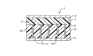
The invention is illustrated by the drawing in which Figure I shows in cross-
section electrical device 1. First electrode 3 is in contact with first resistive element 7,
while second electrode 5 is in contact with second resistive element 13. First resistive
element 7 is made of first polymeric component 9 which acts as a matrix in which is
dispersed first particulate ~lller 11. Second resistive element 13 is made of second
polymeric component 15 through which is dispersed in discrete domains aligned chains
17. Each chain 17 contains particles of second particulate filler 19.
The invention is illustrated by the following examples, each of which was testedusing the Standard lmpulse Breakdown Test.
CA 02239990 1998-06-0~
W O97/21230 PCTnJS96/19319
13
Stslnl1~rd Pevice
Both the first composition and the second composition were prepared by mixing
the clesi~n~ted co~ ollents with a tongue depressor or mechanical stirrer to wet and
disperse the particulate filler. Each composition was deg~se~l in a vacuum oven for one
minute. The second composition was poured onto a PTFE-coated release sheet, and
covered with a second PTFE-coated release sheet separated from the first sheet by spacers
having a thickness of about 1 mm. The outer surfaces of the release sheets were
~U~pOl l~d with rigid metal sheets and magnets with dimensions of 51 x 51 x 25 mm (2 x 2
x 1 inch) and having a pull force of 10 pounds (available from McMaster-Carr) were
positioned over the metal sheets, sandwiching the composition. The second composition
was then cured at 100~C for 15 minute~. The top magnet, the top metal sheet, and the top
release sheet were removed, additional spacers were added to give a thickness of 1.5 mm,
and the first composition was poured onto the surface of the cured second composition.
The top release sheet and the top metal sheet were replaced and a weight (which may be
the top magnet) was placed on top of the top metal sheet. The arrangement was then
cured at 100~C for an additional 15 minutes to give a l~min~te of the first and second
compositions. A disc 20 (as shown in Figure 2) with a diameter of 15.9 mm and a
thickness of 1.5 mm was cut from the cured l~min~t~ The disc 20 consisted of a second
resistive element 21 with a thickness of 1.0 mm from the cured second composition and a
first resistive element 22 with a thickness of 0.5 mm from the first composition.
Molybdenum electrodes 23, 25 having a diameter of 15.9 mm and a thickness of 0.25 mm
(0.010 inch) were attached to the top and bottom surfaces of disc 20 to form a standard
device 27.
St~n~l~rd Tmrulse Rreakdown Test
A standard device 27 was inserted into the test fixture 29 shown in Figure 2. Two
copper cylinders 31,33, ~ loxilllately 19 mm (0.75 inch) in diameter, were mounted in a
polycarbonate holder 35 such that the end faces 37,39 were parallel. One end 37 was
fixed and immobile; the other end 39 was free to travel while still m~ g the parallel
end-face geometry. Movement of cylinder 33 was controlled by barrel micrometer 41
mounted through mounting ring 43. Device 27 was mounted between cylinders 31,33,and micrometer 41 was adjusted until contact with zero compressive pressure was made
to both sides of device 27. Pressure was then applied to device 27 by further moving
cylinder 33 (via micrometer 41) to cOlll~ ,S the sample 10% (generally 0.1 to 0.3 mm).
Electrical leads 45,47 were conn~cte~l from copper cylinders 31,33 to the testing
CA 02239990 1998-06-0~
W O 97/2123~ PCT~US96/19319
14
equipment (not shown). Prior to testing, the insulation resi~t~n-~e R; for the device was
measured at 25~C with a biasing voltage of 50 volts using a Genrad 1864 Megaohm
meter; the initial resistivity Pi was calcnl~t~l Electrical connection was then made to a
Keytek ECAT Series 100 Surge Generator using an E514A IQxlO00 waveform generator.
For each cycle a high energy impulse with a 10 x 1000 ~LS current wavefonn (i.e. a rise
time to maximum current of 10 ~ls and a half-height at 1000 ~LS) and a peak current of
60A was applied. The peak voltage measured across the device at breakdown, i.e. the
voltage at which current begins to flow through the gel, was recorded as the impulse
breakdown voltage. The final insulation resistance Rf after fifty or one hundred cycles for
the standard test was measured and the final resistivity pf was calculated.
Fx~mples 1 to 15
The first and second resistive elements for Examples 1 to 15 were pl~alcd from
compositions using the fnrm~ tions shown in Table I. In each case the silicone gel was
formulated using 49.420% 1000 cs divinyl-t~rmin~tecl polydimethylsiloxane (available
from United Chemical Technology (UCT)), 49.956% 50 cs silicone oil
(polydirnethylsiloxane fluid from UCT), 0.580% tetrakis(dimethyl siloxy silane) (UCT),
0.04% catalyst, and 0.004% inhibitor, all arnounts by weight of the composition. The
stoichiometry was adjusted for peak hardness, i.e. 600 grams using a Voland texture
analyzer with a 7 mm st~inle~ steel probe. The al.l...i~ ,. was a powder with an average
particle size of 15 to 20 microns ( 200 mesh) and a sl-hs1~nti~11y spherical shape,
available from Aldrich Chemicals. The nickel, available from Alfa Aesar, had a mesh
size of -300 mesh and an average particle size of 3 to 10 microns. The arc SU~plcS:iillg
agents, i.e. m~gnç~ium phosphate (Mg3(PO4)2-8H20), zinc phosphate (Zn3(PO4)2 2H20),
calciurn phosphate (CaHPO4 2~20), iron oxalate (FeC204 2H20), and zinc borate
(3ZnO 2B203), the oxidizing agents, i.e. bismuth subnitrate (4BiNO3(0H~2 BiO(OH)) and
lead peroxide (PbO2), and the surge initiators, i.e. calcium carbonate (CaCO3,
decomposition temperature 898~C), m~n~slnese oxalate (MnC204 2H20, decompositiontemperature 100~C), and iron oxalate (which also acts as an arc ~u~lessillg agent,
decomposition temp~,LdLulc 1 90~C), were available from Alfa Aesar. Standard devices
were prepared as above and tested using the Standard Impulse Breakdown Test for either
50 or 100 cycles, as indicated. (Testing for Example 11 was done at lOOA rather than
60A.) In each case, except for colllp~livc Examples 5 and 7, the devices had Ri greater
than 109 ohms. For Examples 5 and 7 the value of R; was greater than 1 o8 ohms. The
CA 02239990 1998-06-0~
WO 97nl230 PCT~US96/19319
average breakdown voltage over the total number of test cycles and the standard deviation
(i.e. a measure of the reproducibility of the breakdown voltage) are shown in Table I.
Examples 1 to 4, which contained an arc ~u~pres~ing agent, showed good low
breakdown voltage (i.e. less than 1000 volts, and, for Examples 2 to 4, less than 400
volts), and good reproducibility. Each had an Rf value of greater than 1 o8 ohms. The test
results for Example 2 are shown in Figure 3.
Examples S to 1 1 show the effects of the presence of both an arc suppressing agent
and an oxidizing agent. Examples 5 and 7, which contained bismuth subnitrate in both
the first and second resistive elements had an Rf value of 1 x 10⁷. When bismuthsubnitrate, which becomes conductive when exposed to moisture, was used in the second
resistive element only (Example 11), the device had an Rf value of greater than 108 ohms,
and excellent reproducibility. Examples 12 to l S show the effects of the presence of a
l S surge initiator. Examples 14 and l S, which contained a surge initiator which had a low
decomposition temperature, had low breakdown voltages and good reproducibility. Each
of Examples 12 to l S had an Rf value of greater than 108 ohms. The test results for
Examples 4, 9, 10, and 1 1 are shown in Figure 4. The test results for Examples 12 to l S
are shown in Figures Sa to Sd, respectively. In each of Figures Sa to Sd results are shown
for three dirrelt;." samples of each type of device. The values reported in Table I are
averages of the three samples for each example.
Monolayer devices which contained only a first resistive element made from a
composition co..'.~il.i.~g alllmimlm powder dispersed in a silicone, shown, for example in
Intern~tional Publication No. WO9S/33278, the disclosure of which is incorporated herein
by reference, had a breakdown voltage of more than 1000 volts when tested using a 10 x
1000 microsecond waveforrn and a current of at most lA. They did not survive fifty
cycles when tested at 60A.
Fx~mple 16
Following the procedure of Examples 1 to 15, a first composition was l,l~ed
coll~ illg 30% al---l,;ol~ 200 mesh), 10% zinc borate, 10% potassium pçnl~ng~n~te~
and 50% silicone gel (as in Example 1), and a second composition was prepared
cont~ining 11.25% nickel with a mesh size of -100 to +200 (available from Alfa Aesar,
with an average particle size of about 100 microns), 3.75% nickel with a mesh size of -
300~ 20% zinc borate, 10% potassium perm~ngs3n~te, and 55% silicone gel (as in Example
CA 02239990 1998-06-05
WO 97/21230 PCTAUS96/19319
16
1), all percentages by volume of each total composition. A Standard Device was prepared
and tested 50 cycles at 60A with a 10 x 1000 microsecond waveform. The average
breakdown voltage was 318 volts, with a standard deviation of 27. Both Rj and Rf were I
x 101 ~ ohms. The test results are shown in Figure 6.
S
Fx~n~le 17
A device was prepared as in Exarnple 16 and tested 50 cycles at 220A with a 10 x1000 microsecond waveform. The average breakdown voltage was 365 volts, with a
10 standard deviation of 32. Both R; and Rf were 1 x 1 ol I ohms. The test results are shown
in Figure 6.
CA 02239990 1998-06-OS
W O 97/21230 PCTtUS96tl9319
17
V~ o ~
o o
o o
o _ ~
o o o o
o o o o o
o o o o
-- o o o o o
ca .~
~ 3 ~ o o o
o o o o o
* o o o o
o o o
o o o
o o o
o o o
_ E E ~ C~ ~ K ~
~ ~ V ~~ V' _ ~ ._
_ _
CA 02239990 1998-06-05
W O 97/21230 PCT~US96/19319
18
V) V~ o ~ o o o o
o ~ ~ o o
~ ~ o ~ ~o cr o o
C~l ~ o ~ ~ oo ~ o
_I ~ o o ~ ~ g og
o ~ ~ o ~ ~ ~ o g
oo o
C ~ o o V~ ~ ~ o o
' C o o
~ o o ~ o ~ o o
o ~ -- ~ ~t ~ ~o _
C~
* ~ o o V~ o o o o
C ~
s ~ o
C ~ O O ~ ~3 et O O
~
~ * ~ o o ~ oo V~ o o
¢
~ ~
~~o ~ ~ o
~ ~ o ~ o~ o O C~
V~ ~ o ~ ~ o o ~
_ ~ ~o O
X
~C 9 g
o ~ ~ ~ ~ o 5
o C o ~ C~
~ ~ Z ~ ~ ~ ~