Note: Descriptions are shown in the official language in which they were submitted.
CA 02240200 1998-06-10 '
GR 95 P 8097
~B c~
~~L~:y ~ 1 ~.;'~
T&~=t""TFiANSLATi~N
Description
Arrangement for triggering a restraint device in a
motor vehicle
The invention relates to an arrangement for
triggering a restraint device in a motor vehicle in
accordance with the preamble of patent claim 1.
Such an arrangement (EP 0 471 871 B1) has an
evaluation device in which a signal supplied by a
sensor device for detecting accidents is evaluated. A
plurality ~of ignition devices distributed spatially
over the vehicle are electrically connected to the
evaluation device via a line/a bus. The evaluation
device supplies to an ignition device alternating
signals which contain messages and which are evaluated
in a logic circuit of the ignition device. Each
ignition device is electrically connected to an
ignition element of a restraint device. In addition, it
is proposed to supply the power necessary for operating
the ignition devices to the ignition devices via the
line.
A known data transmission technology which is
customary everywhere is (amplitude, phase or frequency)
modulation of a high-frequency carrier signal with a
code signal. However, the application of such a data
transmission system in the known arrangement for
triggering a restraint device is disadvantageous since
the modulated carrier signal must supply a sufficient
quantity of power to operate the ignition device, but
owing to the dependence of the transmitted power on the
data it is not possible to ensure a constant power
supply.
In addition, with -such a data transmission
method, the maximum transmittable data rate is limited
by the frequency of the carrier signal. However, since,
inter alia, trigger instructions for triggering the
CA 02240200 1998-06-10
GR 95 P 8097 - la -
restraint device are transmitted an extremely short
data transmission time, and thus a very high data rate,
is necessary for correctly timed
' CA 02240200 1998-06-10
GR 95 P 8097 -
triggering of the restraint device (airbag, belt
retractor and the like). However, a high data rate
requires a high carrier frequency; but the higher the
carrier frequency selected, the stronger the radiated
interference from the line. The disadvantageous effect
of strong radiated interference on electrical circuits
is sufficiently known. This effect is amplified by the
fact that a considerable amount of power for operating
the ignition device is transmitted together with the
modulated carrier signal.
Therefore, the object of the present invention
is to develop further the known arrangement in such a
way that, via the line, it becomes possible to transmit
power and data to the ignition device, which permits a
high data rate and at the same time keeps low the
interference which is radiated onto the arrangement
which is critical for safety.
The invention is achieved by means of the
features of patent claim 1.
Via the line, a static d. c . signal is supplied
to the ignition device whose logic circuit is operated
with the d.c. signal. A message in the form of an
alternating signal is transmitted from the evaluation
device to the ignition device via the same line and, in
the process, additively superimposed on the d.c.
signal. The ignition device contains a filter circuit
for extracting the alternating signal and d.c. signal
from the composite signal transmitted to the ignition
device. The logic circuit which evaluates the
alternating signal is operated with the derived d.c.
signal.
During the transmission of signals according to
the invention, the data transmission rate is
independent of a limit frequency of a carrier signal.
As a result, a trigger instruction can be transmitted
extremely quickly from the evaluation device to the
ignition device. Owing to the low amplitude of the
alternating
' CA 02240200 1998-06-10
GR 95 P 8097 - 3 -
signal in comparison with the amplitude of the d.c.
signal, the radiated interference is negligible even at
high frequencies in the alternating signal. In
addition, the transmission of signals according to the
invention ensures a uniform and continuous transmission
of power during the operating time of the arrangement.
In an advantageous development of the
invention, the ignition device contains a rectifier
circuit by means of which the d.c. signal is fed to the
logic circuit. At the same time, different characters
in the alternating signal have the same frequency but a
different phase relation: the ignition devices which
are distributed spatially over the vehicle are
electrically connected to the evaluation device by
means of a cable harness. Here, the cable harness is
mechanically connected to the evaluation device and to
the ignition devices by means of one plug-type
connector each. During assembly, such a plug-connector
can, through lack of care, be plugged together the
wrong way round, which results in reversed electrical
polarity for components of the ignition device and to
their destruction. Known, but as a rule costly
"polarity reverse protection" circuits in control units
prevent the control unit from being destroyed by such
an incorrectly plugged plug-type connection.
By virtue of the inventive way of transmitting
signals to the ignition device together with the
previously mentioned development of the ignition device
by means of the rectifier circuit and the application
of the so-called diphase method as coding method for
the transmission of the alternating signal, the
ignition device is not only protected against
destruction when plug-type connectors are plugged
together incorrectly in the triggering path, even the
operational capability of the ignition device is
completely retained so that when the inventive
arrangement is assembled it is no longer necessary to
pay attention to the polarity of the plug-type
connections. The rectifier circuit ensures the supply
CA 02240200 1998-06-10
' GR 95 P 8097 - 3a -
of power to the ignition device in all cases with a
correctly
CA 02240200 2001-06-06
20365-3881
4
poled d.c. voltage signal. By virtue of the application of the
aforementioned coding method to the transmission of data for
the alternatlIlg signal, the message contained in the
alternating signal for the ignition device is retained
completely even if ther_~e is a plug--type connection with
reversed polarity: the proposed coding method has the property
that the information in the alternating signal is not in the
high/low (1/0) levels but rather in polarity changes, that is
to say in the phase relation of the individual transmitted
characters. Preferably, the set of characters is binary, the
characters zero and one being phase-shifted by 180° in relation
to one another.
On the other hand, owing to the design of the coding
rule, each alternating signal has an average value of zero,
with the result that the transmitted power depends solely on
the d.c. signal on the line. If the alternating signal were to
have an average value, this would result in a power
transmission which fluctuated aver time. However, the
invention ensures an inventive, uniform transmission of power
so that all the components of the ignition device, and in
particular the ignition element and the ignition capacitor can
have relatively large component tolerances. In addition, owing
to the proposed coding method, the clock frequency on which the
logic circuit is based can easily be derived from the
transmitted alternating signal by the ignition device. In this
way, additional circuitry outlay in the ignition device for
recovering the clock becomes superfluous.
In accordance with the present invention, there is
provided a system for triggering a restraining device in a
motor vehicle, comprising: an evaluation device for evaluating
an impact signal of a sensor for detecting an accident of a
motor vehicle; an ignition device disposed spatially separate
CA 02240200 2001-06-06
20365-3881
4a
from said evaluation device in the motor vehicle; an ignition
element for triggering a restraining device of the motor
vehicle electrically connected to said ignition device; said
ignition device including a logic circuit for evaluating a
message transmitted from said evaluation device, an ignition
capacitor providing a necessary energy for firing said ignition
element; a line electrically connected between said evaluation
device and said ignition device, said line carrying a composite
signal formed by a d.c. signal for operating said logic circuit
of said ignition device and an alternating signal transmitted
additively to the d.c. signal and containing the message to be
evaluated in said logic: circuit; and said ignition device
including a filter circuit for deriving the d.c. signal and the
alternating signal from the composite signal.
Further advantageous developments of the invention
are characterized in the other subclaims.
The invention and its developments are explained in
more detail with reference to the drawing, in which:
Figure 1: shows a block circuit diagram of the
arrangement according to the invention,
Figure 2: shows an injection of a signal onto the
line by the evaluation device,
CA 02240200 1998-06-10
GR 95 P 8097 - 5 -
Figure 3: shows an exemplary signal on the line between
the evaluation device and ignition device,
Figure 4: shows an extraction of a signal in the
ignition device,
Figure 5: shows a circuit diagram of the ignition
device according to the invention,
Figure 6: shows an arrangement according to the
invention which is distributed spatially over
the vehicle,
Figure 7: shows a block circuit diagram of two ignition
devices which are connected to the line, and
Figure 8: shows the coded-diphase method by means of an
exemplary message.
Identical elements are labeled with identical
reference symbols in all the figures. Some of the
reference symbols in Figures 1, 2, 4 and 7 have an F
after them: the elements with such a reference symbol
are predominantly function blocks in block circuit
diagrams in contrast to components/elements of
circuits. Owing to the fact that it is not always
possible to assign components/elements to function
blocks unambiguously, a hierarchical classification of
reference symbols has been dispensed with from the
outset.
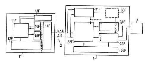
Figure 1 shows an evaluation device 1 which is
electrically connected to an ignition device 3 via a
line 2. The evaluation device 1 contains an arithmetic
unit 11F, a diagnostic unit 13F, a bus coupling unit
14F, a receiver unit 16F, a transmitter unit 15F and a
power supply unit 12F. The ignition device 3 contains a
bidirectional communications interface 32F, a power
management system 31F, a power reserve 33F, a trigger
34F, a diagnostic unit 35F and a non-volatile memory
36F. The ignition device 3 is electrically conductively
connected to an ignition element 4.
The power supply 12F supplies the arithmetic
unit 11F and all the other function blocks of the
CA 02240200 1998-06-10
GR 95 P 8097 - 5a -
evaluation device 1 with power. A signal which is
supplied by
CA 02240200 1998-06-10
GR 95 P 8097 - 6 -
a sensor device (not illustrated) for detecting impacts
is evaluated in the arithmetic unit 11F. The functional
capability of at least the arithmetic unit 11F is
checked by the diagnostic unit 13F.
The evaluation device 1 supplies messages in
the form of coded alternating signals DU to the
ignition device 3 via the line 2. A message can
contain, for example, an encoded trigger instruction
which causes the ignition device 3 to fire the ignition
element 4. A message can also contain measured values,
if for example the final trigger decision is made
before the ignition device 3 itself, status information
of the evaluation device 1 or even commands for the
trigger device 3, in response to which the ignition
device 3 is supplied with status data by the diagnostic
unit 35F, which data are subsequently transmitted from
the ignition device 3 to the evaluation device 1 via
the line 2 and evaluated in the evaluation device 1.
The blocks 16F and 15F of the evaluation device 1
characterize the transmission and reception of messages
in the form of code alternating signals. The evaluation
and compilation of data takes place in the arithmetic
unit 11F which thus not only carries out evaluation
routines but also serves as a bidirectional
communications interface for higher levels of the
communications sequence with the evaluation device 3.
The functional blocks 14F, 15F, 16F in Figure 1
characterize, in this exemplary embodiment, the levels
of the data transmission by the evaluation device 1
which are near to the hardware.
A d.c. signal U is input into the line 2 by the
power supply 12F. The inputting of the d.c. signal U by
the evaluation device 1 is advantageous because the
evaluation device 1 has a power supply in any case. The
d.c. signal U can, as it were, be input into the line
2
on the other side of the evaluation device 1.
CA 02240200 1998-06-10
GR 95 P 8097 - 7 -
Before the d.c. signal U is input into the line
2, the d.c. signal U can be stabilized by means of
circuit technology and regulated to the desired value.
The alternating signal DU is superimposed
additively on the d.c. signal U in all cases. The
composite signal U, U+~U is applied, as voltage,
between the two conductors 21 and 22 of the line 2.
Here, the d.c. signal U is applied to the line 2 during
the entire operating time of the arrangement - that is
to say while the arrangement is activated.
At the ignition device 3, the bidirectional
communications interface 32F performs the derivation of
the alternating signal 0U from the composite signal U,
U+DU and i-ts decoding, processing and, if appropriate,
the conversion of instructions into control signals.
The power management system 31F function
extracts the d.c. signal U from the composite signal U,
U+pU to supply power to the diverse circuit components,
in particular the bidirectional communications
interface 32F. In addition, the power management system
31F function operates a power reserve 33F which is
intended to make available the power necessary to fire
the ignition element 4. This power reserve 33F can also
be used to operate the bidirectional communications
interface 32F for at least a brief period even if the
transmission of power via the line 2 is interrupted.
When a correctly transmitted trigger
instruction is detected, the bidirectional
communications interface 32F actuates the trigger 34F
so that power is transmitted from the power reserve 33F
to the ignition element 4. In addition, the
bidirectional communications interface 32F can cause
the diagnostic unit 35F to check the operational
capability of components and elements of the ignition
device 3, and/or carry out measurements. The
diagnostic, evaluation, -
CA 02240200 1998-06-10
GR 95 P 8097 - 8 -
and coding/decoding rules are stored in the non-
volatile memory 36F.
Figure 2 shows a block circuit diagram of the
inputting of signal components DU, U into the line 2.
Messages are superimposed 143F additively as
alternating signals DU onto the permanently transmitted
d.c. signal U.
Figure 3 shows an exemplary composite signal
U' - U+DU on the line 2. If the evaluation device 1 or
the ignition device 3 have not made any transmission
requests, only the d.c. signal U is on the line 2. In
comparison with the frequency deviation of the d.c.
signal U, the frequency deviation of the alternating
signal 0U is configured to be small in order to avoid a
high degree of radiated interference. Thus, the
frequency deviation of the alternating signal DU is
preferably smaller than 20 percent of the d.c. signal
deviation U, in particular less than 10 percent.
Figure 4 shows a block circuit diagram of the
extraction of the d.c. signal U and of the alternating
signal DU from the composite signal U' - U or U+DU
transmitted on the line. Here, the d.c. signal U is
extracted in the power extraction function block 311F.
Separately from this, the data are extracted in the
data extraction function block 321F and are then
amplified and decoded in 322F.
Figure 5 shows a circuit diagram of an ignition
device 3 according to the invention. Here, in the
ignition device 3, an isolating resistor 34 is arranged
in series with each conductor 21, 22 of the line 2. The
isolating resistors 34 are connected to one another via
a capacitor C1. The isolating resistors 34 are also
connected to the inputs of a rectifier circuit 32 which
is designed as a bridge rectifier 321 and whose outputs
are in turn connected to one another via a controllable
switching means 35. Furthermore, one output of the
rectifier circuit 32 is connected via an isolating
diode 36 to an ignition capacitor 37, and the other
output of the rectifier circuit
CA 02240200 1998-06-10
GR 95 P 8097 - 9 -
32 is connected thereto directly. The terminals of the
ignition capacitor 37 are connected to a logic circuit
33, to two diagnostic devices 39, and to the ignition
element 4 via one further controllable switching means
38 in each case. An isolating resistor 34 is
additionally connected to the logic circuit 33 via a
capacitor C2 and an operational amplifier.
The isolating resistors 34 prevent the entire
bus system (line 2) being short-circuited as a result
of a short circuit in the ignition device 3 caused by
the firing of the ignition element 4 for example, and
it is thus no longer possible to fire at a later time
further ignition elements which have not yet been
fired. In =addition, the isolating resistors 34 prevent
current flowing from the ignition device 3 via the line
2 when the ignition element 4 is fired from the
ignition capacitor 37.
On the other hand, the isolating resistor 34
forms, together with tre capacitor Cl, a low-transmit
filter which filters out high-frequency interference
components in the transmitted composite signal U,U+DU -
but not the frequencies of the alternating signal DU
which contain the messages. Therefore, essentially the
composite signal U,U+DU continues to be present at the
terminals of the capacitor C1. The composite signal
U,U+DU is subsequently rectified by the bridge
rectifier 321. Thus, even when the polarity at the
input of the ignition device 3 is reversed, there is
always a correctly poled composite signal U,U+DU at
circuit components of the ignition device 3 which are
downstream of the bridge rectifier 321.
The isolating diode 36 interacts, as frequency-
dependent resistor, with the power storage capacitor 37
as low-transmit filter. Instead of such an isolating
diode 36, any other frequency-dependent resistor may be
used. The isolating resistor 34 is also decisive for
the filter properties of the low-transmit filter. The
low-transmit filter also
CA 02240200 1998-06-10
GR 95 P 8097 - 10 -
serves as EMC protection against high-frequency
radiation being input into the ignition device 3.
The d.c. signal U which is extracted with the
correct polarity from the composite signal U,U+DU is
present at the terminals of the ignition capacitor 37,
with the result that the ignition capacitor is charged.
Furthermore, the logic circuit 33 and the diagnostic
devices 39 are operated with the d.c. signal U.
Downstream of the isolating resistor 34, the
composite signal U,U+DU is tapped and is fed to a high
transmit filter in the form of a capacitor C2 whose
output supplies the alternating signal 0U which is
converted into a square-wave signal by means of the
operational amplifier OP. As a result the alternating
signal DU is available to the logic circuit 33. The
capacitor C2, isolating diode 36 and ignition capacitor
37 thus form a filter circuit 31 for extracting from
the composite signal U,U+0U the alternating signal 0U
on the one hand, and the d.c. signal U on the other,
the isolating resistors 34 also being responsible for
the low-transmit craracteristics.
The alternating signals DU containing messages
are decoded and evaluated in the logic circuit 33. If
appropriate, calculations are made, measurements
performed, or else the further switching means 38 are
actuated in order to fire the ignition element 4.
If messages are to be transmitted from the
ignition device 3 to the evaluation device 1, the
controllable switching means 35 is fired by the logic
circuit 33. By means of the controllable switching
means 35 the two conductors 21 and 22 of the line 2 are
short-circuited via the isolating resistors 34, with
the result that current flows via the two conductors
21, 22, the isolating resistors 34 and the controllable
switching means 35. This flow of current is detected
and evaluated in the evaluation device 1. Accordingly,
in order to transmit a message comprising a plurality
of characters,
CA 02240200 1998-06-10
GR 95 P 8097 - 11 -
the controllable switching means 35 is actuated by
means of the logic circuit 33 using a bit pattern. This
current modulation for backward transmission of data is
particularly advantageous with the arrangement
according to the invention since only the controllable
switching means 35 is activated by the logic circuit
33: in this backward transmission method no power is
drawn from the ignition device 3. Instead, the power
transmision from the evaluation device 1 to the
ignition device 3 is interrupted. Additional power for
the backward transmission is thus not necessary. This
advantage is essential since the power is transmitted
from the evaluation device 1 to the ignition device 3
and is not available in the ignition device 3 in any
desired quantity. A prerequisite for the backward
transmission of signals which is designed according to
the invention is for the d.c. signal U to be applied to
the line.
Backward signals OR can be read and checked
once more by the logic circuit 33 by means of the
capacitor C2. Thus, a backward signal 0R which has been
read by the logic circuit 33 and has been found not to
be correct is transmitted once more.
The isolating diode 36 is used not only for
low-transmit filtering during the backward transmission
of messages from the ignition device 3 to the
evaluation device 1 - that is to say when the line 2 is
short-circuited via the isolating resistors 34 - but
also to separate the short-circuited line 2 from the
other circuit components of the ignition device 3.
By virtue of the design of the forward and
backward transmission of data and/or power according to
the invention, the arrangement is configured in an
optimum way in terms of its radiated interference and
its expenditure on components, and in terms of the
multiple use of components. -
The controllable switching means 35 is arranged
between the rectifier circuit 32 and the logic circuit
33, with the result that even in the case of incorrect
CA 02240200 1998-06-10
GR 95 P 8097 - lla -
polarity at the input of the ignition device 3 the
communication between the evaluation and ignition
CA 02240200 1998-06-10
GR 95 P 8097 - 12 -
devices 1 and 3 is not adversely affected. Here, a
message which is transmitted from the ignition device 3
to the evaluation device 1 is also encoded in such a
way that different characters have the same frequency
but different phase relation.
The diagnostic devices 39 perform measurements
of the ignition voltage present at the further
controllable switching means 38, and of the resistance
of the ignition element. Furthermore, the operational
capability of the further controllable switching means
38 is checked and leakage resistances in the ignition
circuit (switching path via the further controllable
switching means 38 and the ignition element 4) are
measured. The measurement results are transmitted to
the evaluation device 1, but may also be processed, or
at least preprocessed, in the logic circuit 33 itself .
The operational capability of the logic circuit 33, for
its part, can be checked by the evaluation circuit 1.
Figure 6 shows the arrangement according to the
invention with its components comprising the ignition
devices 3 and evaluation device 1 which are spatially
distributed over the vehicle. The line 2 is represented
here as a bus system.
Figure 7 illustrates an arrangement in
accordance with Figure 6 as a block circuit diagram.
Each ignition device 3 contains the following function
blocks: power extraction 311F, data extraction 323F and
data inputting 322F. On the other hand, at a point in
the motor vehicle which is spatially separated from the
ignition devices 3, data are input 142F and power is
input 141F, respectively. Preferably, these function
blocks are converted in the evaluation device 1.
Figure 8 illustrates the so-called coded
diphase method by reference to a message which is to be
transmitted and which is composed of individual
characters. Figure 8a shows the clock frequency with
which a message is to be transmitted in accordance with
Figure 8b. Figure 8c shows the format in which the
message is ultimately transmitted, the
CA 02240200 1998-06-10
GR 95 P 8097 - 13 -
characters 0/1 in accordance with Figure 8b being
converted by the coded-diphase method into characters
0/1 in accordance with Figure 8c. Zeros and ones which
have been transmitted have the same frequency, but are
phase-shifted in relation to one another by 180°. If,
for example, the character zero is to be transmitted,
it is emitted with the opposite phase relation to that
of the preceding transmitted character, and this means
that there is no change in polarity during a zero.
However, a one does contain a change in polarity.
Such a coding rule has the property that when
the polarity is switched - therefore 8c +U is
interchanged with -U, for example - the message, and
thus the information, is not lost, since the changes in
polarity are decisive in the transmitted signal and not
the polarity/amplitude of the characters. Such coding
methods are also known under the names diphase code or
Manchester code.