Note: Descriptions are shown in the official language in which they were submitted.
CA 0224062~ 1998-06-1~
. .
FILM OR COATING DEPOSITION AND POWDER FORMATION
This invention relates to film or coating deposition and powder formation.
Ceramic, polymer and other films, coatings and powders are used in, for
example, structural and functional electronic applicatiol1s.
As background, the distinction between a film and a coating is ve.y loosely
defined and is not important to the operation or description of the present invention.
In one definition, a film would be considered as a layer under about 10,um thick, and
a coating would be of greater thickness. In the present description, however, the
terrns are generally used interchangeably.
The following are examples of previously proposed techniques for generating
such films, coatings and powders: physical vapour deposition (PVD) (a generic term
- given to a variety of ~ull~lhlg techniques such as radio frequency (RF) ~ulit:lillg,
reactive magnetron sputtering and ion beam sputtering); flame spray deposition
(FSD); the so-called sol-gel process; electrostatic spray pyrolysis (ESP); and chemical
vapour deposition (CVD). Two particular examples are disclosed in EP-A-0 103 505and Applied Physics Letters, Vol. 67, No. 22, Nov. 1995, pp 3337-3339.
However, none of tnese techniques has been found to provide good control of
the stoichiometry morphology, microstructure and electrical properties of
multicomponent oxide films and a relatively high growth rate and deposited area of
a deposited film. Also, the techniques tend to need expensive equipment and highly
skilled technicians for effective operation.
This invention provides a method of depositing a material onto a substrate, the
method comprising the steps of:
(a) feeding a material solution comprising one or more precursor
compounds, a solvent and a pH-modifying catalyst to an outlet to
provide a stream of droplets of the material solution,
(b) generating an electric field to electrostatically attract the droplets from the outlet towards the substrate; and
(c) providing an increase in temperature between the outlet and the
substrate.
AM~NDED SltEFI
CA 0224062~ 1998-06-15
Further respective aspects of the invention (to which the various preferred
features are equally applicable) are defined in the appended claims.
Embodiments of this method, which will be referred to hereinafter as
electrostatic spray assisted vapour deposition (ESAVD), enable the fabrication of both
S thin and thick films. The technique combines the advantages of CVD and electrostatic
spray deposition whilst alleviating the problems associated therewith. In comparison
to other film deposition techniques, ESAVD has a high deposition rate and efficiency,
and allows easy control of the stoichiometry and microstructure of the deposits. In
addition, it is a simple, cheap, and low-temperature synthesis method suitable for the
10 fabrication of a variety of different films. The method also allows the deposition of
a film on large surface area substrates.
The use of the pH-modifying catalyst (which can be acid or alkali) can provide
a clearer solution with increased electrical conductivity, and so can give finer droplets
and thus a better coating quality.
The method can be performed in so that the substrate and other pieces of
apparatus are open to the surrounding ambient atmosphere, the other ambient gaseous
reactants refer to any other gaseous reactants (such as oxygen, for example) that may
be present in the atrnosphere. In another embodiment, the method may performed
within the confines of a container and said other ambient gaseous reactants may be
supplied to said container, thereby to enable the deposition of a particular film.
Both simple and multicomponent ceramic oxide films have been fabricated
using the above mentioned method. In one embodiment, the film may be a ceramic
film such as PZT (Lead Zirconate Titanate) or a doped film such as YSZ (Yttria
Stabilised Zirconia). Other films may include PbTiO3, BaTiO3, La(Sr)MnO3, NiO-
YSZ, SnO2-InO3 and other Indium-Tin Oxide films. The film may also be a
AMENDED SHEET
CA 0224062~ 1998-06-l~
WO 97/21848 PCT/GB96/03105
Figure S is a flow chart illustrating steps in a polymer deposition process;
Figures 6a and 6b illustrate X-ray diffraction patterns for polymer films
produced by two process variants;
Figures 7a and 7b illustrate L~ iU~nce infra-red spectra for polymer films
produced by the two process variants;
Figures 8a and 8b illustrate surface reflectance infra-red spectra for polymer
films produced by the two process variants;
Figures 9a and 9b are schematic diagrams showing dipole orientation in
polymer films produced by the two process variants;
Figure 10 schematically illustrates a third embodiment of a~y~ldLus for materialdeposition;
Figure 11 illustrates a fourth embo~liment, used for powder deposition;
Figure 12 (curves a and b) show x-ray diffraction patterns for the nano-
powders produced at 500~C and 800~C respectively; and
lS Figure 13 and 14 show the microstructures of YSZ nanopowders at different
reaction Lelllp~dLulc;s.
In a first embodiment a coating solution is deposited to form a cerarnic film
on a substrate.
A film deposition ~paldlu~ as shown s~hem~tically in Figure 1 comprises an
outlet (e.g. a no~le, spray or similar~ 5 connected to a high voltage DC source 7
preferably variable in the range 0-30 kV. In operation, a voltage of between 5 and 30
KV would be normally used for the ~alus as shown. A substrate holder 4 is
earthed and is heated by a heater 2. The t~ln~ldlulc of the ~lb~kdL~ holder 4 iscontrolled by the controller 1 and an s~ hpcl thermocouple 3.
Heating the substrate holder also causes a corresponding heating of the area
surrounding the substrate 14 and between the substrate holder and the outlet 5. This
heating serves to set up a temperature gradient whereby the arnbient temperatureir.creases as the substrate is approached from the direction of the outlet. Thisincreasing temperature facilitates a chemical vapour reaction (see Figure 3) of the
coating solution that enables deposition of the cerarnic film.
When an electric field of sufficient strength is applied to the outlet 5, a corona
field is produced from the tip of the outlet 5. A ceramic coating liquid is used to
CA 0224062s 1998-06-1~
W O 97/21848 PCT/~B96/03105
structural and/or functional film such as an electroceramic film.
Preferably, the droplets are charged to a voltage within the approximate range
j-30 kilovolts with respect to the substrate.
In one embodiment, the L~lnpeldL lre increases gradually to a temperature in theSapproximate range 100 to 650 degrees celsius (the temperature used may depend on
the type of coating). Varying the processing pararneters enables the production of
denselporous and/or thin/thick films all of which have good adhesion to the substrate.
Preferably, the film has a thickness between a nanometre and approximately
100 micrometers, or much thicker.
10In any of the above embodiments, the catalyst may be an acid such as ethanoic
acid or hydrochloric acid. In this case, the required pH may ~e between 2 and 5.Alternatively, the catalyst may be an alkali such as NH3. In this case, the
required pH may be b~Lw~ell 9 and 12.
The invention can be particularly useful for producing polymer coatings, in
15which case it is preferred that the electric field is n-Ai.,~ ed during at least part of the
time during which the substrate cools down after coating has been performed. This
can urge the polymer into a desirable polar structure.
The appardlus may further comprise a syringe purnp or a static pres~le feed
to provide a constant stream of coating solution to said outlet.
20The a~pdrdlus may also comprise a container capable of enclosing at least saidsubstrate and said outlet, such that other gaseous reactants may be supplied forreaction with said coating solution.
The invention will now be described, by way of example only, with rer~,e~cc
to the acco~ dllying drawings in which:
25Figure ~ illustrates schem~tiç~lly an a~d~aLus for use in electrostatic spray
assisted vapour deposition of a film on a substrate;
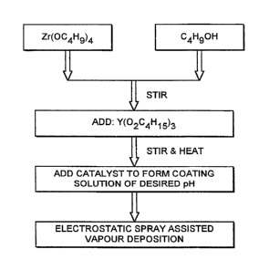
Figure 2 is a flow chart that illustrates sch~m~sically steps in the synthesis of
coating solution for the electrostatic spray assisted vapour deposition of YSZ;
Figure 3 srh~m~tically illustrates the principle of electrostatic spray assisted30vapour deposition of a film from a coating solution using the apparatus of Figure l;
Figure 4 schem~tically illu~lidles another embodiment of apparatus for use in
electrostatic spray assisted vapour deposition;
CA 0224062~ 1998-06-l~
WO 97/21848 PcT/Gsg6/03l05
form the films and is fed into the outlet 5 in the direction indicated by an arrow 6.
The outlet's inner diameter can vary from lmm (millimeter) to 0.1mm. This
relatively large inner diameter reduces the chances of clogging problems when high
viscosity solutions are passed through the outlet 5.
A substantially constant flow in the range of 0.4 - 60 m~lh (millilitres per hour)
is m~int~ined by use of a syringe pump or a constant static ~ ule feed.
In this way, the electrostatic field set up between the charged outlet 5 and theearthed ~ub~ildlt: holder 4 serves to guide charged coating solution droplets to the
substrate 14. Droplets of the coating solution are provided with a positive charge by
way of the high voltage DC source 7. These positively charged droplets are attracted
to the earthed substrate holder 4. (As an ~ltern~tive, of course, the droplets could be
negatively charged with an earthed holder 4, or vice versa).
Figure 2 sch~m~tically illu~Llales steps in the ~l~a dLion of one type of coating
solution for the deposition of YSZ (Yttria Stabilised Zirconia~. First, a y~e~u~o~
compound (in this case, Zr(OC4H934 ) is mixed with a solvent (in this case, Butanol -
C4HgOH). This solution is stirred and a second precursor compound Y(02C4HI5)3
(more generally, a metal alkoxide or an organometallic compound) is added under
action of heat. The mixture is then catalysed to form a coating solution of the desired
pH. In this case, ethanoic acid (CH3COOH) is used as a catalyst, but other acids (such
as HCI) or allcalis (such as NH3) may be used in the ~fe~d dLion of ~It~rn~tive coating
solutions. In the case of acid catalysed reactions, the desired pH may be between 2
and 5. In the case of alkali catalysed reactions, the desired pH may be l)~L~ n 9 and
12.
The coating solution, a mixture of Zr(OC4H9)4, Butanol and Y(O2C4HI5)3, is
then passed to the outlet 5 and discharged towards the substrate 14.
Preferably, the concentration of the desired coating solution is approximately
0.01-0.5 mol/l (moles per litre). In addition, the coating solution may have a viscosity
in the region of about 0.01 to 50 mPa.S (millip~c~l seconds) depending on the type
of film that it is desired to produce.
Table I shows the compositions of coating solutions for various deposited
films.
CA 02240625 1998-06-15
WO 97/21848 PCT/GB96103105
O O
Cr~ ¢ ¢ ¢ ¢ ¢ ¢ ¢ ¢ ~ ~;
C s~ s~ C ~ ~: ~ ~
.S ~ ~ V V
C'~ ~~ ~~, ~ o -t 3 ~
c :C :C ~ O ~ m ~ 5 0 ~ O
U~ O O O ~ o~ ~ O O O O _
V V ~ ~ ~ ~ ~ o ~
o o
o
O O
~ o
~ ~ V~ V V Z V V
0, 0 0 U~ l ~ ~ '~ ~
O ~ 0~ 0 O,~ rl o ~ ~~1
'Eii _, ~ D
~LL,
~, ~ .a
a ~ O ~ ~ ~ ~ ~ ~O ~ Vx
G ~9 0~ ~ ~ ~ ~ V ~ x
C~
CA 02240625 1998-06-15
WO 97/21848 PCT/GB96/03105
In table 1, the composite ~le~;ul~ol~ with alkoxide precursors are so-called "sol"
precursorsl. The precursor compounds are mixed in relative quantities ap~lol,liate to
the desired stoichiometry of the desired film. Sufficient catalyst is added to give the
coating solution the required p~I.
Ethanoic Acid is a pler~ d catalyst to provide a clear solution, an improved
solution conductivity and therefore finer spray droplets. However, other acids andlor
alkalis such as hydrochloric acid, arnrnonia, nitric acid, Lewis acid or sodium
hydroxide would all be suitable catalysts.
Acid or base catalysts can influence both the hydrolysis and con~ n~t;on rates
and the structures of the con~l~ncecl products. Acids serve to protonate negatively
charged alkoxide groups, enh~ncing the reaction kinetics and elimin~ting the
~uh~lent for proton transfer within the transition site. Therefore, acid-catalysed
c~ Pn~tion is directed ~lcf~l~lllially towards the ends rather than the middles of
chains, resulting in more e~t~n~ fl, less highly branched polymers. Alkaline
conditions produce strong nucleophiles via deprotonation of hydroxo ligands.
B~e-catalysed con.1~nc~tion (as well ~ hydrolysis) should be directed toward themiddles rather than the ends of chains, leading to more compact, highly branchedspecies. Hence, if porous films of good quality (e.g. a&esion and porosity) are
required, aLcalis are ~ler.,~l.,d as catalysts.
Similarly, various other inorganic or organic solvents can be used such as
alcohol, water, or a mixture of alcohol and water could be used.
Figure 3 srh~ ti~ y illustrates the principle of electrostatic spray assisted
vapour deposition of a film from a coating solution.
The Le~ peldLu~e preferably increases, on passing from the outlet to the
2~ substrate, from about 100~C to between 400 and 650~C. At point (I) on Figure 3, the
coating solution forms a corona spray, the droplets of which are charged to a positive
potential. As the droplets are attracted to the substrate 14 they begin to form clusters
' The term Sol-gel is used to describe chemical processes in which polymeric gels
are formed from metallo-organic starting solutions (see for exarnple: "Sol-gel Science"
by C.~effrey Brinker and George W. Shearer, published in 1990).
SllL..a ~ JTE SHEET (RULE 26)
CA 02240625 1998-06-15
WO 97/21848 PCT/GB96/03105
together (shown at point (II) in Figure 3) under the influence of an increased arnbient
Lc~ cl lwe. At point (III) in Figure 3, the clusters decompose and/or react in close
proximity to the substrate to form the desired ceramic film. The clusters may also
react with other gaseous reactants such as oxygen. For exampie, the
hydrolysis/con(len~tion reaction for the production of a Sol~gel transition is as
follows:
Hydrolysis: _M-OR + H20 ~ eM-OH + ROH
Contl~n~tion: aM-OH + RO-M_ ~ =M-O-Me + ROH
=M-OH + HO-M- ~ =M-O-M- + H20
Where M is the desired metal film element (in this case of YSZ, Zirconium)
and R is CnH2n+l~ e.g. C4Hg. In this method, the chemical reaction proceeds forwards
(towards the right hand side of the above equations) and the reaction time decreases,
with increasing te~ ldLul~. Thus, the hydrolysis/conrlçn~tion reaction is speeded up
with increasing temperature.
The substrate and other pieces of a~dlus are open to the surrounding
ambient atmosphere, and so the other ambient gaseous reactants refer to any other
gaseous re~ct~nt~ (such as oxygen) that may be found in the atmosphere. In another
embo~lim~nt, the technique may performed within the confines of a container, and any
desired arnbient gaseous re~ct~nt~ (such as hydrogen sulphide, for example) may be
introduced into that container. These introduced gases may react with the clusters to
forrn particular films (such as sl-lrhicle or nitrite films, for exarnple) on the substrate.
To s~mmS~ e, during ESAVD, droplets of coating solution are charged and
then transform into clusters or fine particles between the discharge outlet 5 and the
substrate 14. This transformation occurs under the action of a corona field and an
increasing lcll~ dLule towards the substrate. These clusters and fine particles are then
attracted to the substrate by virtue of the induced electric field. The temperature
gradient is such that the clusters and other gaseous reactants coexist around the
substrate 14. The precursor clusters undergo decomposition and/or chemical reaction
with gaseous re~ct~nt~ just on or in very close plo~ y to the substrate surface.Chemical reactions involving coating precursor clusters cause the formation of the
desired ceramic film - as illustrated in Figure 3.
As this method operates on a principle whereby charged droplets from the
CA 02240625 1998-06-15
WO 97/21848 PCT/GB96/03105
outlet 5 are attracted towards a grounded substrate, it is particularly suitable for
sC~nning o~ writing large surface areas and is not restricted to particular chamber sizes
as in CVD and PVD. Growth rates achievable with this method were found to be
between 0.1 and 5 microns per minute depending upon the concentration and flow rate
of coating solution. ~igher growth rates are possible by further altering the deposition
conditions.
The achievable microstructure, grain size, composition, surface morphology and
thickness of ceramic film are strongly dependant on the process conditions. The grain
size in the deposited film is mainly ~ , .";..e~l by the droplet size, and the flow rate,
viscosity and concenkation of coating solution and subskate IC111~)C1dLU1~:. Forexample, the grain size of ceramic films increases and uniformity of the grain
distribution decreases as the droplet sizes, flow rates, concentration, substrate
Lc~ cldlulc and viscosity of coating solution increase. Similarly, droplet sizes are
mainly detf rrnint-(l by the corona field intensity and coating liquid conductivity. The
mean droplet size decreases with increasing coating liquid conductivity. Thus, films
with n~no~i7P grained microstructure can be deposited with the ESAVD technique.
The crystal phase ~lluclulcS of the deposited cerarnic films are mainly
det~rrnin~cl by the lclllpc~dLulc of the subskate 14. Ceramic films formed at lower
substrate temperatures, have an amorphous or nanocrystalline crystal phase. These
films may then be treated by an additional ~int~ring process, to kansforrn the crystal
skucture from an amorphous or nanocrystalline skucture to the desired ceramic phase.
A higher substrate tcll~peldLulc during deposition results in an increase in crystallinity
of the cerarnic film deposited thereupon.
Other films, such as simple oxide films, multicomponent oxide films (e.g. PZT
(Lead Zirconate Titanate - Pb(ZrxTi~ x)03 ), PbTiO3, BaTiO3, Indium Tin Oxide orLa(Sr)MnO3) or doped films (e.g. YSZ (Ytkia Stabilised Zirconia -
(ZrO7)092(y2o3~oo8 ) or Ni-YSZ) etc, structural and/or functional films such as
electroceramic films, nanostructured films, and/or of course films other than ceramics,
may be produced with this technique.
Referring back to Figure 1, because the tenll)GldLul~ gradient gen.. dL~d by the
proJections of the substrate holder 14 towards the outlet 5 is not necessarily constant
in front of the subskate 14 in the plane of the substrate, the uniformity of coating
CA 0224062~ 1998-06-l~
WO 97/21848 PCT/GB96/03105
thickness can be improved by rotating and/or tr~n~l~ting (in general, moving) the
outlet and/or the substrate holder during deposition to vary the relative positions of the
outlet and the substrate with time. If rotary motion is used, this could involve, for
examp}e, rotating the substrate (which might be three-dimensional) about an axispassing through the substrate, or possibly rotating the outlet (or outlets, if more than
one is used) about an axis which is not coaxial with the outlet's axis (i.e. "circling"
the outlet around).
In another feature, the polarity of the electric field applied between the outlet
and the substrate holder can be reversed from time to time during the depositionprocess. This can be beneficial to avoid the ~cc~lmlll~tion of charges (which can
coulll~-dct the effect of the applied field), thus allowing thicker coatings to be
produced.
"Graded" coatings can be produced by varying the concentration and/or
composition of the ple~;ulsor solution during deposition. (Simply, this can be achieved
by depositing the collL~llL~ of a first container (bottle) of precursor solution, and then
switching to another container and so on).
Similarly, it has been found that films may be produced of a thickness varying
from a nanometre to approximately 100 micrometers in thicLn~c~ (or much thicker).
The coatings can be used in microscale ci~cuiL-.y or for much bulkier items such as
turbine blades for jet engin~s, by scaling up the a~pd,dlus (the apparatus of Figures
1 and 4 as shown has a substrate diameter of about 20mm).
Single crystal substrates can be used to obtain oriented or epitaxial films. A
range of microstructures including epitaxial, columnar and equiaxial growth are
possible by varying the processing conditions.
The substrates may be conductive (e.g. metal) or non-conductive (e.g. glass,
polymer or ceramic).
Another embodiment of an electrostatic spray assisted vapour deposition
(ESAVD) ~dLus is s~heJn~tically illustrated in Figure 4.
The apparatus of Figure 4 is similar to that of Figure 1, except that a shaped
substrate holder 104 projects towards the outlet 5 at either side ofthe substrate 14'.
The substrate holder 104 is heated as before, and this heating serves to set up a
t~.npe.dLulc gradient whereby the arnbient temperature increases as the substrate IQ6
CA 0224062~ 1998-06-l~
WO 97/21848 PCT/Gs96/03105
is approached ~rom the di}ection of the outlet 107. (The arrangement of Figure 1 also
provided an increase in temperature approaching the substrate 14 from the direction
of the outlet 5, but the arrangement of Figure 4, with the projecting parts of the
substrate holder 104, provides a more gradual t~ e~dLule gradient). This increased
S temperature and more gradual t~n~ gradient facilitates solvent evaporates and
decomposit;on of the coating solution near the vicinity of the substrate that enables
deposition of the film.
The use of the appalaL~s of Figure 4 (or indeed, Figure 1) to produce PVDF
polymer coatings on the substrate will now be described.
The improvement of the performance of polymer films, and the ability to
fabricate specif1c bulk polymer with tailored surface compositions for particular
application have become hllpol~ considerations. The need for rl~igning polymer
with well-controlled chemical compositions at the surface arises from the fact that
i.,L~lracial phenomena define ~ Lies that are crucial to the service perform~nce of
a particular device. ~xamples of applications where polymer surface properties are
hll~o,L~ll include wetting, printing, biomedical and electronic devices. In all these
cases, molecules from the "ellviiol~nent" approach the polymer surface and experience
interfacial forces due to electrostatic and positive/or negative charged cloud
interactions. It thus becomes possible, in principle, to design guided approaches
towards device o~Lh~-i~Lion by controlling polymer film growth in order to alter or
control interfacial interactions of polymers by the provision of ~,o~.;ate chemical
structure in the surface layers.
Surface modif1cation techniques have been used widely in polymer industry.
The techniques of flame tre~tment acid etching, and corona discharge treatment after
~5 the fabrication of the bulk polymer materials have been used ~ ,c Lt;"~iv ;;ly in intlllctri~l
applications, produce a variety of new polar surface. This is quite acceptable in
wetting and printing applications, but for applications of polymers in electronic and
biomedical devices, the presence of a polar surface is not sufficient. The ~lignment
of polar groups in polymer films along preferred orientation need to be considered as
well. Plasma surface treatment techniques have the advantage for the surface
modification of commodity polymer substrates, but the penetration depth of the
treatment is very low at a reaction level for useful surface modification. Meanwhile,
CA 0224062~ 1998-06-1~
WO 97t21848 PCT/GB96/03105
the equipment of plasma technique is very expensive and needs highly skilled
technicians.
A typical example for the polymer depositions is to fabricate the piezoelectric
and pyroelectric polyvinylidene fluoride (PVDF) film. PVDF film has a large
dielectric constant, due to the large dipole moment of CF2, and is one of the most
polar dieleckic polymers. Its advantages over ceramic materials include light weight,
flexibility, tollghness, ease of fabrication and low permittivity. The conventional
fabrication of PVDF films for electronic application normally involves two production
steps. Firstly, PVDF bulk films are produced by a conventional method such as cast,
hot pressing, dipping and spin coating of PVDF solution. Then, PVDF buLk films are
treated by the modification techniques such as high thermal high voltage poling,corona poling, stretching and electron beam discharge etc. However, the deposited
PVDF films cannot be stretched, it is difficult to prepare ~-phase crystal film by this
method. On the other hand, the breakdown of thin films occurs easily under a high
electric field. As a result, it is not easy to pole thin PVDF films. In the present
technique, the film production and surface modification poling of polymer PVDF films
can be achieved in a single production step.
Therefore, in this application, the outlet's inner diarneter preferably reduces
towards the outlet's tip from about lmm to about 0.1rnm. This relatively large initial
inner diameter ensures that the likelihood of clogging problems with high viscos;ty
solutions (such as PVDF) in the outlet 5 is significantly reduced.
A ~ul~L~llially constant flow of PVDF coating liquid to the outlet S is
m~in~ined by use of a syringe or pneumatic pump (not shown). Preferably, the
solution flow is in the range of 0.4 - 10 ml/h.
In this way, the electrostatic field set up b~Lwee.~ the charged outlet 107 and
substrate holder 104 serves to guide charged coating solution droplets to the substrate
14'. As described earlier, droplets of the coating solution are provided with a negative
charge by way of the high voltage DC source 1. These negatively charged dropletsare thus attracted onto the substrate and in moving towards the substrate pass through
a region of increasing temperature gradient. The t~ c~dLu~e gradient ensures that the
solvent evaporates before the PVDF precursor droplets reach the suhstr~t(~ 14' and the
chemical reaction occurs just on or in very close vicinity of the substrate surface to
CA 02240625 l998-06-l5
WO 97/21848 PCT/GB96/03105
form a PV13F crystal phase film coating.
After the PVDF film coating has been applied, the syringe pump can be turned
off and heating can be stopped. The PVDFfilm coated substrate is then cooled down
up to room t~ GldLulc, with the electric field m~int~;ned during this cooling process.
Figure 5 is a flow chart illustrating steps in a polymer deposition process.
Referring to Figure 5, a ylGcul~Jl solution used to deposit the films of PVDF
comprises a mixture of poly vinylidene fluoride (PVDF) powder and solvent
N,N,-Dimethylform~mi~le (DMF) or N,N,-Dimethyl~et~micle (DMA). As a first step,
PVDF powders are dissolved in DMA or DMF solvent. This solution is stirred and
heated at 60~C for thirty minlltes. A clear solution with 0.01 to 0.1M concentration
in PVDF is yielded. Then, acetic acid CH3COOH is added into the solution as
catalyst according to pH 2 to 5 and conductivity range greater than or equal to 2.0,us
at room temperature. After thirty minutes stirring, a clear ylec~llaor solution for
PVDFfilm coating is obtained.
Although there is no complete agreement among investigators ,e~udi~-g the
me~h~ni~m responsible for piezoelectricity and pyroelectricity in PVDF, there is nearly
~m~nim( us agreement that a polar crystal form is required for o~i",w~, activity. One
of the complicating factors about PVDFis that it can exist in four dirr~LG~ll crystal
forms. The crystal phase in which the chain conformation is trans-gauche-trans-
gauche is called a-phase. The chains are then packed in a monoclinic unit cell which
is non-polar.
A variety of techniques have been employed to form PVDF films into a second
crystal phase called ,B-phase in which the chain c~,llr~,L"lation is es~enti~lly all trans
and the chains cryst~lli7~1 in an orthorhombic unit cell with a net dipole moment.
It is thus lcnown that there are at least two stable crystal forrns of PVDF, a
planar zig-zag polar form (a-phase) and T-G-T-G non-polar form (~-phase). One can
obtain an oriented ~-form from the a-form in PVDF films by mechanical stretchingor rolling, corona discharge, and high l~;;llly~ re high voltage poling. A nurnber of
l~:se~ucl1el~ have shown that the ~-form is very ilnpoll~l,L in obtaining good
piezoelectricity and pyroelectricity in PVDF films.
Since the ~-form crystal exhibits a net dipole moment, the present process uses
the inventors' observation that molecular dipoles on chains within the crvstalline
CA 0224062~ 1998-06-1~
WO 97/21848 PCT/GB96tO3105
14
regions of the polymer become aligned with the applied electric field during the poling
process and are then relatively stable in such an orientation in the absence of the
piezo- and pyro electric response. Only the crystalline regions of the polymer would
become perms~n~ntly aligned and then only that component of the chain axis which lies
S in the plane of the film would be expected to contribute to the polarisation.
For identifying the influence of corona field in trials of this process, in fact two
experiment~l processes were compared. In the first case, the corona field was turned
off while samples were cooled down to room t~ e~aLu~e after deposition (process I).
In the second case, the corona field was ~ ;tit~efl while sarnples were cooled down
to room temperature after deposition (process II), to m~int~in the dipole orientation
of the deposited material in a required orientation until the material solidified.
X-ray diffraction patterns of the PVDF film produced under process I and
process II are shown in Figures 6a and 6b respectively. The diffraction peak observed
at 2~3~20.8~ is ~eciEn~cl to unresolved (110) and (200) diffraction of ,B-phase in PVDF.
a-phase in PVDF shows diffraction peaks 2~18~ ~ignPd to (100), (020) and (021)
respectively. The comparison of process I with process II shows that the intensity of
main peak at about 20.8~ increases under corona field. It in~lir~t~ that some parts of
a-phase have transformed into ,~-phase in PVDF. This result was confirm~cl by
respective infra-red (IR) spectra, as shown in Figures 7a (Process I) and 7b (Process
II) for tr~nemieeion spectra, and Figures 8a (Process I) and 8b (Process II) forreflectance spectra.
Many journal papers have reported on the crystal forms of PVDF from IR
spectra. The a- and ,B-phase crystal forms have many common absorption band
characteristics (such as CH,CH2, CF,CF2, and C-C etc.) as reported in the literature.
It is known that the crystal forms can be identified by the characteristic absorption
bands of ,~-phase at about 510 and about 1280 cm~l, and that of a-phase at about 530,
about 610 and about 795 cm~l.
From the results of IR analysis between process I and II, it is clear that the
contents of ,B-phase is higher in the PVDF film produced using process II, but acertain amount of a-phase may still exist under process II. It int~ tes that PVDF
films prepared by process II consist mainly of the ,~ crystal phase with some a-phase.
meanwhile, it is also found that corona field strongly influenced the surface structure
CA 0224062~ 1998-06-1~
WO 97/21848 PCT/GB96/03105
of PVDF film. From the spectra, it is observed that since the absorption peak at about
1280 cm~l in process II is assigned to the CF2 syrnmetric stretching vibration of ,B
crystal phase, and is stronger than that in process 1, the results of the IR spectra
suggest that ~-form crystal is oriented and the CF2 dipoles are aligned along the
applied corona field.
There have been many investigation of a-phase and ~-phase crystal in PVDF
film. it is well known that the a-phase crystal is more stable than the ~-phase crystal.
The reason why the ,B-phase crystal was formed in spite of its instability was not clear.
In the present case of ESAVD, it is proposed that the stability and the m~ch~ni~m of
~-phase crystal formation is as follows. Because ~-phase crystal is the polar crystal,
~B-phase is stabilized and formed in ~r~l~nce to a-phase when the corona field exist
during the deposition of PVDF film. Consequently, the content of ~-phase increases
with increasing the energy supplied to the ~ul~ dle by the corona discharge. Under
the conditions shown in the experim~nt~l section, the charge droplets of the PVDF
solution were attracted onto the substrate and the PVDF film was formed by
evaporation of the solvent and decomposition of ~ uL~UI solution during substrate
temperature field. PVDF polymer seems to have enough mobilitv to change the
conformation aligned along the applied field direction under the existence of the
corona field during evaporation of the solvent. But if the corona field does not exist
after deposition (as process I), a certain amount of energy is obtained to rearrange the
PVDF molecules because the substrate Len~.dLul~ is high enough near/or over PVDFmelting point 1 70~C. In contrast, when the corona field exist during cooling down of
the PVDF film to room telllpcld~ule~ the polar groups in PVDF film are "cooled"
along the applied corona field direction.
Figures 9a and 9b are schematic diagrams showing dipole orientation in
polymer films produced by the two process variants, process I and process II. These
illustrate that under process II a PVDFfilm with oriented ,B-phase crystal, which is
very important for getting good piezoelectricity and pyroelectricity in PVDF film.
The present studies thus show that the oriented thin PVDFfilm can be ~ ~ed
directly onto a substrate in single step by a novel ESAVD technique. The corona field
ism~int~int?d during ~ub~Lldl~ cooling to form oriented polar polymer film PVDF, but
other forms of PVDF can be produced without m~ g the field. The corona field
CA 0224062~ l998-06-l~
WO 97/21848 PCT/GB96/03105
helps to transport the charge droplets of PVDF solution onto the substrate to form
PVDF thin film, and forces the polar group in PVDF thin film to align along the
corona field.
In conclusion, the utilization of corona field in the vapour deposition process
S is effective in controlling crystal forms and their orientation, to foIm polar polymer
films.
The present results also clearly revealed the potentials of this technique to
deposit polymer thin film of good quality with a very simple eql-irm~nt This
technique can be used in the fabrication of a wide range of polymer films, including
polar and conductive polymer/or co-polymer coatings, such as PVDF, PTF~,
po1y~nilinec, and polypyrrole etc.
Figure 10 illustrates a third embodiment of a deposition a~p~aLus. In many
,e;,~.e~ , the ~)~aldLuS of Figure 10 is similar to that of Figure 4, but for the ~ lition
of deflectors 210 under the control of a deflection controller 200.
The deflectors are used to deflect the spray of electrically charged droplets
emerging from the outlet. This can steer or concentrate the spray on particular desired
areas of the ~ubsL.dL~, or move the spray distribution around to help to colll~eLlsdle for
an uneven lem~ldlul~ gradient near the substrate. The deflectors can be electrostatic
plates, in which case the deflection controller supplies a high voltage between the
plates to deflect the electrically charged spray emerging from the outlet, and/or
magnetic deflectors (eg a yoke coil or other winding), in which case the deflection
controller supplies a current to coils in the deflectors to g~ lale a magnetic field to
deflect the charged spray.
In other embollimentc, the substrate could be heated to a t~ ldlUL~ just below
that required for film deposition (e.g. 50~C below that required for film deposition3.
If a laser beam is then directed onto the substrate by a suitable beam-steering
mech~nicm and used to heat very localised areas of the substrate while the solution is
being sprayed from the outlet, deposition will occur selectively at those areas of the
substrate.
In further alternative embodiments, m~cking can be used to mask off certain
areas of the substrate to give control over where the film is deposited.
Figures l l to 14 relate to the use of these techniques to generate powders,
CA 02240625 l998-06-l5
WO 97/21848 PCT/GB96/03105
rather than films or coatings. The example to be described is that of YSZ powders,
but many other materials (particularly the materials described above with reference to
the film or coating techniques) could be used.
The dirr~ Liation between film (coating) production and powder production,
using basically the same ~dld~, is mainly one of t~ p~,ldLul~ (although other
operational parameters can be varied). If the ambient l~ llp~,~dLl.Ll~ between the outlet
and the substrate is increased then the droplets of coating solution will tend to forrn
powder particles before hitting the substrate. This effect can be exaggerated byslowing down the flight of the droplets - e.g. by çh~ngin~ the flow rate or the electric
field - to give more time for the powder to form. Alternatively, if a cold substrate is
used, then the droplets will con-i~nee into powder particles on hitting the substrate.
Figure 11 illu~L-~Les a suitable d~ lLdLUs for m~ f~rturing the powdered YSZ.
The d~dLus comprises a tubular, up-flow reactor e~luipped with an f ~t~rn~l resistive
heater. YSZ sol p-~,u~or is delivered at an ~lul~liate flow into a st~inless steel
capillary outlet (100 ~m inside ~i~m~ter, 650 ,um outside diameter) which is
d at a dc voltage of 10-30kV (positive polarity). The capillary electrode is
placed 15-30 mm from a ring electrode m~int~ined at lkV dc voltage. The functionof the ring electrode is to focus the spray aerosol into the reactor charnber and select
the ~ .iate n~no~i7Pd particles to reach the ~ub~LIdl~. The high local electrostatic
field at the capillary tip causes an emission of charged aerosol from the highlydeformed liquid int~rf~ce A stream of Argon gas from a coaxial glass capillary (800
~Lrn inside diameter) carries the spray charged aerosol through the ring electrode into
the reaction zone of the reactor, finally to arrive at the cold substrate (having a
negative polarity).
The YSZ sol precursor with monodispersed nanosize particles is synth~ci7~d
as follows. First, Y(NO3)3.6H20 is dissolved in 2-propanol while stirring for about
15 min at room te...pe.dLIlre yielding a clear solution. Zirconium tetra n-butoxide,
Zr(OC3Hg)4 is added into the previous solution according to the stoichiometry of a
desired final composition of (ZrO2)0 92(Y~O3)0 08. The final sol precursor
concentration and pH are preferably 0.05M and 3-5 respectively. The hydrolysis and
con~l~n~tion can be carried out at room temperature under stirring.
The YSZ nanoparticles produced by a prototype of this technique were
CA 02240625 1998-06-15
WO 97/21848 PCT/GB96/03105
analysed using x-ray diffraction and tr~n~mi~ion electron microscopy ~TEM).
The quality of the YSZ nanopowders depends strongly on the process
conditions. Below a reaction tel~lp~,~dlule of 4~0~C, all samples appeared to beamorphous from the x-ray diffraction traces. Figure 12 (curves a and b) shows x-ray
diffraction patterns for the nano-powders produced at 500~C and 800~C re~l.ecli~ely.
The x-ray diffraction patterns show that fully stabilized cubic zirconia (YSZ)
nanopowders are directly formed. The plesence of monoclinic or free Y2O3 phases
were not detecte~l in YSZ powders produced at about 500~C. No other new phases
were observed. It in~lic~tPs that Y203 has been perfectly dissolved into the ZrO2
lattice to form a solid solution.
Figure 13 and 14 show the microstructures of YSZ nanopowders at dirr~rc.ll
reaction lclllp~ldlulcs. In the nanopowders formation process, the YSZ aerosol is
produced by electrostatic assisted spray, and delivered into reaction zone in CVD
reactor charnber, the fine droplets of aerosol change into dry gel and pyrolysis to forrn
the nanopowders onto cold substrate under an a~p,~,~.;ate low temperature. TEM
rnicrographs reveal that the distribution of YSZ nanoparticles is ulLifollll and the
average size of YSZ powders deposited at 500~C is 10-20nrn (Figure 13). Under the
high reaction lclllpcldluLc (e.g. 800~C), particle-cluster aggregation occur. This is
because aerosol droplets changed into particles at high reaction ~c~llpeldLLLLcS~ TEM
micrograph reveals that the diskibution of YSZ nanoparticles is not uniform and the
YSZ particles size is in the range of 30-80 nanometres at high LcllLpcLdLulcs (Figure
14).