Note: Descriptions are shown in the official language in which they were submitted.
CA 02240967 1998-06-18
HARTING KGaA
Marienwerderstr. 3 1998-05-13
D-32339 Espelkamp 9720 CA P 9
Plu~ connector for card-ed~e mountin~
The invention relates to a plug connector for card-edge mounting, in particu-
lar a plug connector with 2 or more rows for SMD connection to a printed cir-
cuit board, wherein the printed circuit board connection side of the plug con-
nector has at least one press-on body which is connected to the insulating
body of the plug connector so as to be capable of rotating or hinging and in
which the soldering connections of the contacts of the plug connector are
held.
It is known practice to mount surface-mountable components on both sides
of a printed circuit board. For reasons of space, the surface-mountable
components (surface-mounted devices, SMD) are kept very low in height
and small in order to be able to accommodate as many components as pos-
sible on one printed circuit board and in order to keep the assembly low in
height.
The so-called "surface-soldering technique" (surface-mounted technology -
SMT) was developed as a substitute for the conventional soldering-in tech-
nique, in order to simplify the automatic fitting of printed circuit boards withelectronic components. In this technique, deposits of solder are applied to
surface regions (soldering pads) of the printed circuit boards by means of
solder pastes, in which the connection contacts of the components are verti-
cally immersed. In the process, special automatic fitting machines fit and
position the surface-mountable components (surface-mounted devices,
SMD's) in the correct location on a printed circuit board. The soldering of
the complete printed circuit board then takes place in a soldering installation.In the case of a board fitted with components on both sides, the said board is
9720CA~.DOC
CA 02240967 1998-06-18
turned over and the second side is provided with solder paste, fitted with
components and soldered.
In order to connect the printed circuit boards to the rear wall printed circuit
board of a slide-in frame or rack, the predominant practice is to mount plug
connectors by the pressing-in technique, or else multi-row SMD plug connec-
tors which build up vertically, on the printed circuit board. As a result of this,
the width of installation of a slide-in SMD assembly is subsequently deter-
mined only by the height of the plug connectors. The extra space gained by
means of the surface-mounted components is thus lost again because of the
relatively"large" plug connectors.
An electrical connector for card-edge mounting for connection to the surface
of a printed circuit board is known from DE 195 11 508 A1, in which the
printed circuit board connection side has a press-on body which is con-
nected to the insulating body of the connector so as to be capable of hinging
and in which the contact connections of the connector are held.
In addition, a plug connector for card-edge mounting is known from DE 195
30 994 C1, in which contact springs rest on contact faces on the printed cir-
cuit board when the latter is in the inserted state.
Furthermore, a connector for printed circuit boards which has a press-on
body which presses resilient contact elements onto a flat electrical conduc-
tor, is known from DE 38 22 980 C2.
The underlying object of the invention is to construct a plug connector of the
initially mentioned type in such a way that the said connector can be at-
tached to the printed circuit board by surface mounting, is simple to mount
and, at the same time, has a low structural height.
This object is achieved through the fact that the plug connector is opened in
a "jaws-like" manner for the mounting process, while a releasing mechanism
9720CA-O.DOC
CA 02240967 1998-06-18
opens the press-on body, against the spring force of the contact springs, for
the insertion of the printed circuit board, that at least one side of the solder-
ing connections of the contacts is pressed against the printed circuit board
by means of the press-on body on the rotatably mounted side, and that the
pressing-on force of the press-on body is applied by the spring force of the
contact springs.
Advantageous refinements of the invention are indicated in claims 2 to 9.
The advantages obtained with the invention consist, in particular, in the fact
that the plug connector according to the invention has a high contact density
and the printed circuit board provided therewith has only a low structural
height, while optimum space-utilization of the current card height (320 con-
tacts/100 mm) is achieved through the simultaneous use of both sides of the
plug-in card. A further advantage lies in the symmetrical arrangement of the
plug connector in relation to the daughter card (straddle mount).
The plug connector also has the same installation conditions as existing 2.0
mm and 2.5 mm "hard metric" plug connector systems, and integratability
into existing SMD mounting installations, and also automatic fixing of the
plug connector on the printed circuit board until soldering takes place, are
likewise provided.
The connection of the printed circuit board (daughter card) to a rear wall
printed circuit board (backplane) via the plug connector by the surface
mounting technique meets the requirement for components which are ever
lower in height. The plug connector can be constructed with 2 or more rows.
An exemplified embodiment of the invention is represented in the drawings
and will be described in greater detail below. In the drawings:
figure 1 shows a view of a plug connector,
9720CA-ODOC
CA 02240967 1998-06-18
figure 2 shows the view of the plug connector with the press-on body
hinged open and latched, and
figure 3 shows the view of the plug connector with the press-on body
unlatched, and
figure 4 shows a view of the plug connector according to figure 2, in
section along the line 4 - 4, and
figure 5 shows a view of the plug-connector according to figure 3, in
section along the line 5 - 5.
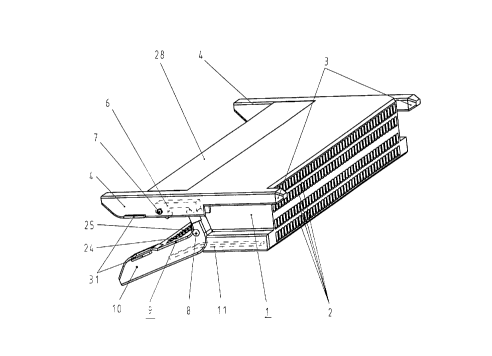
Figures 1 to 5 represent the insulating body 1 of a plug connector, which
body consists of plastic and has a multiplicity of contact chambers 2 let into it
in two or more rows. In this instance, the plug connector is constructed as a
so-called "SMD plug connector" for surface mounting on or against a printed
circuit board. Attached laterally to the end face of the insulating body 1 are
two guide elements 3 which ensure pre-centering of the plug connector
when the latter is plugged together with a matching plug, for example a ter-
minal strip (of which no further details are represented here). Located lat-
erally on the rear side of the insulating body 1, that is to say the printed cir-
cuit board connection side, are two flanges 4. The flanges 4 are provided
with chambers 5 which are open on at least one side. In the said chambers
5, there is provided a releasing mechanism 6 which, as represented in the
figures, is rotatably mounted in a bearing 7 on the insulating body 1. Also
located laterally on the insulating body 1 are two bearings 8. Rotatably
mounted on the insulating body 1 in the bearing 8 is a press-on body 9
which likewise consists of insulating plastic. Two flanges 10 are likewise
attached to the press-on body 9 on the rear side. By means of the releasing
mechanism 6, the press-on body 9 is hinged open and opened in a "jaws-
like" manner for the insertion of a printed circuit board, as represented in fig-
ures 1, 2 and 4. In the process, the releasing mechanism 6 latches in this
9720CA-ODCC
CA 02240967 1998-06-18
open position. The press-on body 9 is pre-tensioned by springs 11 which
are located in the flanges 4 and 10.
The contacts 16, 17, 18, 19, which are preferably designed as double-
legged, twisted contact springs, are held in the insulating body 1 in the re-
gion of the fixed seats 12, 13, 14, 15. The contacts 16, 17, 18, 19 consist of
the following regions: the contact tulip 20, 21, 22, 23, the fixed seat 12, 13,
14, 15, and the soldering connections 24, 25, 26, 27.
o Mounted on the rear side of the insulating body 1 is an insulating guide body
28 consisting of plastic. The soldering connections 26 and 27 of the con-
tacts 18 and 19 are guided in the guide body 28, and the soldering connec-
tions 24 and 25 of the contacts 16 and 17 in the press-on body 9. Because
of the guide body 28 and also of the press-on body 9, very high coplanarity
of the contacts 16, 17, 18, 19 in the region of the soldering connections 24,
25, 26, 27 is achieved and, at the same time, a defined depth of impression
into the solder paste 29 on the printed circuit board 30. Four metallically
solderable fastening flanges 31, which are soldered to the printed circuit
board 30 after the mounting of the plug connector, are fastened in the
flanges 4 on the insulating body 1 and in the flange 10 on the press-on body
9. The fastening flanges 31 absorb the tensile forces and insertion forces
produced when the plug connectors are plugged in and pulled out.
Figures 2 and 4 show, in side view and also in section, the mounting state of
the plug connector, with the press-on body 9 hinged open and latched.
What is represented is a plug connector in which the press-on body 9 is
mounted at one end, for rotation with the insulating body 1, in the bearing 8.
The plug connector is pushed laterally onto a printed circuit board 30 and
positioned in the correct location.
During the placing of the plug connector on the upper side of the printed cir-
cuit board 30, the releasing mechanism 6 is released and unlocks the
hinged-open press-on body 9, which is pre-tensioned by the spring 11. Be-
9720CA-ODOC
CA 02240967 1998-06-18
cause of the position of the bearing 7 in conjunction with a pivotable point on
the releasing mechanism 6, which point acts, when the press-on body is
hinged on, on the upper side of the printed circuit board and exerts an axial
force component, the plug connector is drawn against the end face of the
printed circuit board 30. At the same time, the plug connector is fixed on the
printed circuit board 30 by the spring force of the soldering connections 24,
25, 26, 27 of the contacts 16, 17, 18, 19 or by additional springs 11, until
soldering takes place.
Figures 3 and 5 show, in side view and in section, the final state of the plug
connector with the releasing mechanism 6 unlocked and the press-on body 9
hinged on.
During the production process, the fitting of the printed circuit board with theSMD components takes place by sides, that is to say only one side of the
printed circuit board is provided with solder paste, then fitted with surface-
mountable components and soldered. In the case of a printed circuit board
which is fitted with components on both sides, the said board is then turned
over and the second side is provided with solder paste, fitted with compo-
nents and soldered. In the process, the connection contacts of the surface-
mounted components must be pressed into the solder paste perpendicularly
and with a defined depth. Another condition in the surface-mounting tech-
nique, which condition is determined by the automatic fitting machines them-
selves, is force-free or low-force mounting of the components. In order to
meet both conditions in the case of a plug connector with 2 or more rows
which, moreover, is not to build up to too great an extent, it is necessary to
assist the low mounting force of the automatic machine by means of an ad-
ditional spring force which, after the release of the releasing mechanism 6,
presses the movable press-on body 9 against the printed circuit board 30.
Under these circumstances, the necessary spring force can be generated by
the contacts 16, 17, 18, 19 or by additional springs 1 1.
9~20CA-O.DOC
CA 02240967 1998-06-18
In order to bring this about, the soldering connections 24, 25, 26, 27 of the
contacts 16, 17, 18, 19 of the plug connector are guided in a guide body 28
or in the press-on body 9. This is necessary in order to guarantee very high
coplanarity. At the same time, the soldering connections 24, 25, 26, 27 of
the plug connector are pressed, with a defined depth, into the solder paste
29 on the printed circuit board 30, and the plug connector is simultaneously
fixed on the said printed circuit board 30.
For the process of soldering the plug connector, it is necessary for solder to
be provided, as a fixed deposit of solder, on at least one of the two soldering
connections 24, 25 or 26, 27 of the contacts of the plug connector. An im-
portant point in this connection is that, in the case of boards fitted with com-ponents on both sides, the second side of the printed circuit board can be
provided with solder paste only after the first side has been completely fitted
with surface-mounted components and soldered.
9720CA-O DOC