Note: Descriptions are shown in the official language in which they were submitted.
CA 0224l0l0 l998-06-l9
H6481, 6-293
Adaptive Pre-Distortion Ap~aldllls for Line~ri7in~ An Amplifier Output Within a Data
Tran~missil)n System
The present invention relates to comll,ul ication systems and is particularly directed
to a system for coLu~lelacting the non-linear behavior of a high-power amplifier of a
transmission system.
A broadcast ~:ollunul ication system employs a high-power amplifier as part of a signal
5 Iral~ll,is~ion or transponder section of the system. U1~U1 lullalely, a highpower amplifier has
non-linear distorting characteristics that cause distortion of the information signal which is
amplified. The non-linear distorting characteristics of the high-power amplifier can impact
the instantaneous amplitude and phase of the signal significantly. Or~y so much can be done
to "linearize" a high-power amplifier due to cost and power dissipation.
0 Known techniques are used to "pre-correct" an information signal in order to linearize
the output of the amplifier. One of these techniques includes amplitude correction which
produces a linear piece-wise pre-correction function which is correlated to the non-linear
characteristics of the amplifier. The result is a piece-wise correction curve which approximates
the ideal correction. The correction is added to the information signal.
It is also known to use an information signal to address a RAM which contains
predetermined, pre-distorted versions of the information data values as disclosed in the
specification of U.S. Patent No. 4,291,277. The pre-distorted version is supplied as a signal,
in lieu of the actual information signal, to components (e.g., a quadrature mixer) which feed
into the tran~mi~ n amplifier. The substitute values in the RAM are updated via an analog
20 ~:Olll~dl;SOl:l between a representation of the actual, desired data and a demodulated, "sliced'l
(or re-quantized) sample signal from the amplifier. The sample signal is provided for the
comparison via suitable components (e.g., a quadrature demodulator) along a feed-back path.
However, the known system is limited by the values output by the quadrature mixer
and the quadrature demodulator. For example, for a system employing a 16 QAM,
25 quadrature demodulation of the sample signal is limited to one of four levels in each of the
real (I) and imaginary (Q) axes. The known system does not have the ability to provide certain
spectral corrections. Also, the analog comparison is limited by resolution of the analog
signals. Specifically, the slicer of the demodulator does not provide information between
sample periods (i.e., there is no useful information available). The know system cannot correct
30 for out-of-band distortion. Thus, the know system cannot correct for the non-lin~?aritif~
induced by an amplifier onto a 32 bits-per-word PAM signal in an eight vestigial sideband
CA 0224l0l0 l998-06-l9
H6481, 6-293
system (8VSB). In particular, QAM is quantized to a limited set of levels in each of the I (real)
and Q (imaginary) axes. In contrast, 8VSB is quantized in the I (real) axis, thus, the Q axis is
infinitely variable.
The present invention includes an adaptive apparatus for compensating a distorting
5 action to information signals by a transmission amplifier of a wide band transmission system,
the amplifier subjecting the signals to shifts in signal characteristics away from their intended
values, said apparatus comprising: signal provision means for providing a multi-bit digital
information signal, memory means for storing a plurality of digital pre-distortion correction
values, selection means for selecting a pre-distortion correction value in said memory means
lo using a predetermined number of significant bits of the information signal as a memory
address, combiner means for digitally combining the i~ aLion signal and the selected pre-
distortion correction value to provide a pre-distorted signal, supply means for supplying the
pre-distorted signal to an input of the amplifier, sampler means for coupling off a sample
signal, resulting from amplification of the pre-distortion of the information signal, from an
15 output of the amplifier, comparison means for ~ompalillg the information signal and the
sample signal in digital format, and update means for modifying the selected pre-distortion
correction value in said memory means based upon the ~:ompalison by said comparison
means.
Conveniently, the adaptive apparatus for compensating a distorting action to
20 i ~ ion signals by a ~ n~ n amplifier of a wide-band transmission system, has the
amplifier subjects the signals to shifts in signal characteristics away from their intended
values. The apparatus includes data provision means for providing a multi-bit digital
information signal. Memory means stores a plurality of digital pre-distortion correction
values. Selection means selects a pre-distortion correction value in the memory means using
25 a predetermined number of significant bits of the information signal as a memory address.
Combiner means digitally combines the information signal and the selected pre-distortion
correction value to provide a pre-distorted signal. Supply means supplies the pre-distorted
signal to an input of the amplifier. Sampler means couples off a sample signal, resulting from
amplification of the pre-distorted information signal, from an output of the amplifier.
30 Comparison means ~ Jares the information signal and the sample signal in digital format.
Update means modifies the selected pre-distortion value in the memory means based upon
the comparison by the comparison means.
CA 0224l0l0 l998-06-l9
H6481, 6-293
-
The invention will now be described, by way of example, with reference to the
accompanying drawings, wherein:
Fig. 1 is a srh~m~ti( illustration of an apparatus;
Fig. 2 is a schematic illustration of an example device;
Fig. 3 is a schematic illustration of a portion of the device shown in Fig. 2 which
contains the apparatus;
Fig. 4 is a plot of an amplifier transfer curve; and
Fig. 5 is a complex vector plot illustrating the pre-distortion correction of the present
invention.
lo Fig. 1 shows an a~aldLus 10 which compensates for distortion of information data
signals. The apparatus 10 according to the present invention provides pre-distortion
correction for information data which is transmitted at a relatively high rate. Further, the
present invention is useful for wide band applications (e.g., 18 MHz).
The high data rate and bandwidth are related to the system envi~ollll,ent in which the
15 apparatus 10 is utilized. Accordingly, the apparatus 10 may be used in any system having
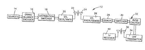
such 11~m~nl1ing requirements. For example, the apparatus 10 is utilized in a high dl~finition
(HDTV) system 12, as shown in Fig. 2. The HDTV system 12 includes a plurality of sources
14, such as a camera unit, a storage unit, or a receiver unit (e.g., a satellite downlink). Signals
from the sources 14 are provided to a grand alliance encoder 16. The signal from the grand
20 alliance encoder 16 is provided to a distribution switcher 18 which provides a signal to a STL
multiplexer/transmitter 20.
A microwave link is established between source and remote microwave antennas 22
and 24, and a signal from the remote antenna 24 is provided to a STL receiver/demodulator
26. The signal proceeds through a ~mllltiplexer 28 and a switcher 30, to an eight (8) vestigial
25 sideband (hereinafter 'l8VSB") exciter 32. The 8VSB exciter 32 (Fig. 3) ~:ol~ s the apparatus
10 in accordance with the present invention. The output of the 8VSB exciter 32 (Fig. 2) is
provided to a UHF/VHF ~lal SlnlUel' 34, and a broadcast signal from a broadcast antenna 36
is received at a television 40. It will be appreciated by a person of ordinary skill in the art that
signal timing lines, which supply applopl;ate timing signal to various components of the
30 system (including components of the apparatus 10) are needed for synchronizing operation
of the various components. The person of or.lil~ y skill in the art will understand the timing
operation. Accordingly, the timing lines are omitted for clarity.
CA 0224l0l0 l998-06-l9
H6481, ~293
-
Turning now to the details of the example 8VSB exciter 32 shown within Fig. 3, the
information data stream is received from the switcher 30 and proceeds to a byte formation
device 42 and then to a byte randomizer device 44. The information data stream proceeds
through a Reed Solomon encoder 46 and through a Trellis encoder 48. The information data
5 stream proceeds through one or more filters and/or correctors 50, an adaptive non-linear
corrector 52, and one or more filters and/or equali~ers 54. In the preferred embodiment, the
information data stream input to the non-linear corrector 52 is comprised of 32-bit words
defined within a phase-amplitude modulated electrical signal. The non-linear corrector 52 is
part of the apparatus 10 which compensates for non-linear distortion of the information signal,
0 and is described in greater detail below.
The information data stream proceeds through a digital-to-analog COllV~l Lt~l (DAC) 56
and an up converter 58, which is driven by a local oscillator 60. The information data stream
proceeds from the up converter 58 toward the transmitter 34. Within the transmitter 34, the
information data stream (now analog and up-converted) is passed through a high-power
tran~mi~ion amplifier 62 of the tran~mi~t.or 34. The amplifier 62 distorts the signal passing
through the amplifier in a non-linear fashion.
For example, Fig. 4 is a plot of a LldnsLel function (i.e., input vs. output) of a high-
power amplifier. An actual transfer curve of the amplifier is shown by a solid line in Fig. 4.
A linear Lldlls~l curve, which is typically an ideal that is not achievable, is shown by the dot
20 line of Fig. 4. The plot shows the deviation of the actual transfer from the ideal as the input
increases.
As part of the process of compensating for the non-linear distortion caused by the
amplifier 62, the output of the amplifier 62 is "sampled" to provide a feed-back sample signal.
The feed-back sample signal is indicative of the amplifier output and is provided along a feed-
25 back path. Specifically, a coupler 64 couples off the sample signal from the output of the
amplifier 62. The feed-back sample signal passes through a down converter 66, which is
driven by the same local oscillator 60 as the up converter 58. The feed-back sample signal
passes through an analog-to-digital converter (ADC) 68 and is provided to the non-linear
corrector 52.
Within the non-linear corrector 52 (Fig. 1), in order to compensate for the non-linear
distortion caused by the amplifier 62, the il~lmdLion signal (i.e., the source data signal, which
is hereinafter referred to as the original information signal) is pre-distorted. Specifically, the
desired output from the amplifier, upon amplification of the pre-distorted signal, is a signal
CA 0224l0l0 l998-06-l9
H6481, 6-293
which would occur if the amplifier 62 did not cause distortion. Further, as the distortion
properties of the amplifier 62 change (e.g., change due to temperature fluctuation, and change
due to aging of components), the non-linear corrector 52 adapts the pre-distortion to
compensate for the new distortion from the amplifier 62.
In the non-linear corrector 52, the original information signal is provided to a real-to-
complex converter 70. It should be appreciated that if the original information signal is
supplied to the non-linear corrector 52 in complex format (I,Q), the real-to-complex converter
70 is not needed. For example, a real-to-complex conversion of the original information signal
may occur up-stream of at least one of the filters/correctors 50, which operates in complex
lo rather than real. For purposes of discussion is this specification and not limitation, the data
stream supplied to the non-linear corrector 52 is real and the real-to-complex converter 70 is
present.
The output of the real-to-complex converter 70 is an I-channel signal, which is
representative of the real component, and a Q-channel signal, which is representative of the
15 imaginary component. In the ~re~red embodiment, the I-channel original information signal
contains 16 bits per word (i.e., one-"half" of the original 32 bit word), and the Q-channel
original information signal contains 16 bits per word (i.e., the other "half" of the original 32 bit
word).
The I-channel original information signal is supplied as a first input to an I-channel
20 summation device 72I and the Q-channel original information signal is supplied as a first
input to a Q-channel summation device 72Q. A second input to the I-channel summation
device 72I is provided from an I-channel random access memory 74I. Similarly, a second
input to the Q-channel summation device 72Q is provided by a Q-channel random access
memory 74Q. Within each of the sllmmA~ n devices 72I, 72Q, the two supplied inputs are
25 added.
The values provided by the I-channel and Q-channel memories 74I and 74Q to the
summation devices 72I, 72Q are pre-distortion correction values. Each of the I-channel and
Q-channel memories contain an array of memory locations, which are in the form of look-up
tables. Each memory location c~ ail s a correction value word, which has a size
30 corresponding to the I/Q original information signal word size. Accordingly, in the ~refelled
embodiment, each word within the I-channel and Q-channel memories has 16 bits.
Preferably, the array size (i.e, number of memory locations) of the I-channel memory
74I is identical to the size of the Q-channel memory 74Q. The array size of the I-channel and
CA 0224l0l0 l998-06-l9
H6481, 6-293
Q-channel memories 74I and 74Q is related to the number of bits of each information data
word which are designated as "most significant". Specifically, the size of each of the I-channel
and Q-channel memories 74I, 74Q is 2kl x 2k2, wherein kl is a number of designated most
signifirant bits of the I-channel original information signal and k2 is a number of designated
5 most significant bits of the Q-channel original information signal. In the preferred
embo~1im~nt, for each channel (I and Q) eight bits (of the 16 total bits) are designated most
significant. Thus, preferably, the memory arrays (I and Q) each have 28 x 28 (65,536) memory
locations, and the size of each memory (I and Q) is (28 x 28)*16.
The correction values in the I-channel memory 74I are accessed and supplied to the
lo second input of the I-channel S~ ." ,~1 ion device 72I by utilizing the k-most significant bits of
the I-channel original information signal word, plus the k-most significAnt bits of the Q-
channel original information signal word as an address. The k-most significAnt bits of the I-
channel original information signal word are provided on an address bus 76I through a buffer
connection 78I (e.g., appluplial~ tri-state buffer illL~ ections). The k-most significant bits
15 of the Q-channel original information signal word are provided on an address bus 76Q
through a buffer connection 78Q (e.g., ap~n~liate tri-state buffer interconnections). Within
the I-channel memory 74I, the k-most significant bits of the I-channel original information
signal is used as the k-most significant bits of the memory address and the k-most significant
bits of the Q-channel original information signal is used as the k-least significant bits of the
20 memory address. It will be appreciated that the accl~ssing the I-channel memory 74I is
controlled via an address bus buffer controller, which is omitted for clarity, and a read/write
control line.
Similarly, the correction values in the Q-channel memory 74Q are accessed and
supplied to the second input of the Q-channel summation device 72Q by utilizing the k-most
25 significant bits of the I-channel original information signal word, plus the k-most significant
bits of the Q-channel original information signal word as an address. Within the Q-channel
memory 74Q, the k-most significant bits of the I-channel original information signal is used
as the k-most significant bits of the memory address and the k-most significant bits of the Q-
channel original information signal is used as the k-least signifi~ant bits of the memory
30 address. It will be appreciated that the ac~ssing the Q-channel memory 74Q is controlled via
an address bus buffer controller, which is omitted for clarity, and a read/write control line.
The addition of the correction value provided by the memory 74I to the I-channeloriginal information signal (via the sl~mmA*nn device 72I) results in a pre-distorted, I-channel
CA 0224l0l0 l998-06-l9
H6481, 6-293
,.~lmaLion signal. The addition of the correction value provided by the memory 74Q to the
Q-channel original information signal (via the sl~mm~tinn device 72Q) results in a pre-
distorted, Q-channel information signal. The present invention provides for, not only
correction of signal amplitude distortion, but also correction of il~ldn~ eous phase distortion
5 caused by the amplifier 62. Accordingly, the values in the memories have complex factors
which are accessed by use of the Q-channel original il-[olll~Lion signal as part of the memory
address.
The pre-distorted I-channel and Q-channel signals are output from the summation
devices 72I and 72Q, respectively. The pre-distorted I-channel and Q-channel signals are
0 provided to a complex-to-real C~ vt~l L~l 80. The converter 80 combines the I-channel and Q-
channels, and outputs a pre-distorted information signal, in real format. The output of the
complex-to-real converter 80 is provided to the digital-to-analog converter 56 to proceed
downstream, through the up COllv~l lel 58 to the transmitter 34 with its amplifier 62. The pre-
distorted information signal output from the complex-to-real converter 80 is such that the non-
15 linear distortion, caused by the amplifier 62, is compensated.
Adaption to the changing non-linear distorting characteristics of the amplifier 62 is
accomplished via provision of the feed-back sample signal (i.e., the pre-distorted, distorted
signal output from the analog-to-digital converter 68) to the non-linear corrector 52. Within
the corrector 52, the feed-back sample signal is input to a real-to-complex converter 82. The
20 output of the real-to-complex converter 82 is an I-channel feed-back sample signal and a Q-
channel feed-back sample signal. The I-channel and Q-channel feed-back sample signals
represent the pre-distorted, amplifier-distorted original information signal in the complex
domain. In the pre~ll~d embodiment, the I-channel and Q-channel feed-back sample signals
comprise 16 bit words.
A correction al~,ol;Lhll, 84 adapts or adjusts the amount of pre-distortion which the
non-linear corrector 52 imposes upon a subsequent ill[ullndLion data signal. The I-channel and
Q-channel original information signals, which are output from the real-to-complex converter
70, are provided as a first input to the correction algorithm 84. The I-channel and Q-channel
feed-back sample signals, which are output from the real-to-complex converter 82, are
30 provided as a second input to a correction algoliLl~lll 84. Within the correction algulillul- 84,
the I-channel original information signal is compared with a corresponding I-channel feed-
back sample sign~l to determine a difference. Preferably, one of the two compared I-channel
signals is subtracted from the other. Similarly, the Q-channel orig-inal information signal is
CA 0224l0l0 l998-06-l9
H6481, 6-293
~:oln~ar~d with a corresponding Q-channel feed-back sample signal to determine a difference.
Scaling of the I-channel and the Q-channel original information signals takes place, if
necessary, within the correction alguliLl,lll 84 to accommodate system gain variations.
Because the non-linear corrector 52 is a component within a data stream system,
5 subsequent, 'loriginal" ~ ~ If ollllation data continues to move through the system and must be
processed. Also, the feed-back sample signal which corresponds to a particular original
information signal is "created" when that original information signal passes through the
amplifier 62 (i.e., coupled off of the output of the amplifier). The feed-back sample signal is
created at a time later than the provision of the corresponding original information signal to
0 the correction al~,uriLhlll 84. Further, the corresponding feed-back sample signal must proceed
and be processed through several components to reach the correction alg-)liLlul- 84.
Accordingly, the correction al~,oliLhlll 84 includes buffer memory means (not shown) for
holding each the I-channel and Q-channel original information signals for a short duration
until they are matched for comparison with the corresponding I~hAnn~l and Q-channel feed-
15 back sample signals. The original information signals (I and Q) are held in the buffer memoryawaiting the completion of the activity regarding provision of the corresponding feed-back
sample signals (I and Q) to the correction al~,olilllm 84 (again, timing signals, necessary to
correlate and synchronize, are omitted for clarity).
Focusing now on the ~:olll~alison between the corresponding signals within the
20 correction alg()lillllll 84. The differences, if any, between the original information signals (I
and Q) and the feed-back return sample signals (I and Q) represent the proportional amount
that the original information signal should have been pre-distorted in order to fully
compensate for the distortion which occurred within the amplifier 62. This can be understood
by identifying the original information signal as an "A" vector (Fig. 5) in a complex plane and
25 identifying the feed-back sample signal as a "B" vector in the complex plane. The difference
between the A and B vectors is a "C" vector. The "C" vector represents the error vector which
identifies the direction and relative magnitude of the correction needed.
The correction algulill,m 84 generates a new I-channel correction value and a new Q-
channel correction value for adjustment of the values in the I-channel and Q-channel
30 memories 74I and 74Q accordingly. If necessary, the new I-channel and Q-channel values are
scaled. The new correction values are supplied by the correction algorithm 84 to input lines
86I, 86Q of the I-channel and Q-channel memories 74I and 74Q, respectively. ~imultAneously,
the correction algorithm 84 provides an eight bit address for each of the I-channel and Q-
CA 0224l0l0 l998-06-l9
H6481, 6-293
channel memories to be applied to the address bus lines 76I and 76Q, respectively. The
memory addresses provided by the corrected al~,ulillull are derived from the original I-
channel and Q-channel signals stored within the buffer memory of the correction alg~lillu
84.
When the distorting characteristics of the amplifier 62 change, the correction al~,ol;llu
84 will successively refine the correction values within the I-channel and Q-channel memories
74I and 74Q each time an identical original information signal proceeds through the data
stream. In other word, the process is iL~idliv~ or empirical. The amount of correction (i.e., the
vector C, Fig. 5) which the correction algolillull 84 generates will become smaller and smaller
o as the correction progresses toward ideal pre-distortion correction values. Further, each time
the distorting characteristics of the amplifier 62 change, the adaptive non-linear corrector 52,
with *s correction algorithm 84, adapts to the new distortion.
Accordingly, the present invention provides finer transfer curve control and
adaptation to system changes (e.g., drift). Further, inter-symbol levels created by pulse
15 shaping and/or system bandwidth limiting are corrected. Specifically, inter-sample levels are
accommodated via a sample rate greater than the symbol rate.
An adaptive ap~aral~ls for compensating the non-linear distorting action of an
amplifier in a transmission system. I-channel and Q-channel memories store a plurality of
digital pre-distortion correction values. The memories are addressed using a predetermined
20 number of significant bits of an incoming, original information signal to retrieve I-channel and
Q-channel pre-distortion correction values. The I-channel and Q-channel pre-distortion
correction values are combined, digitally, with I-channel and Q-channel components of the
original information signal to pre-distort the original information signal. The pre-distorted
signal, in real format, is supplied to the amplifier, and a feed-back sample signal is coupled-off
25 of the output of the amplifier. A comparison is made between the original information signal
and the feed-back sample signal in digital format and in the complex domain (I/Q).