Language selection

Search

Patent 2241083 Summary

Third-party information liability

Some of the information on this Web page has been provided by external sources. The Government of Canada is not responsible for the accuracy, reliability or currency of the information supplied by external sources. Users wishing to rely upon this information should consult directly with the source of the information. Content provided by external sources is not subject to official languages, privacy and accessibility requirements.

Claims and Abstract availability

Any discrepancies in the text and image of the Claims and Abstract are due to differing posting times. Text of the Claims and Abstract are posted:

  • At the time the application is open to public inspection;
  • At the time of issue of the patent (grant).
(12) Patent Application: (11) CA 2241083
(54) English Title: METHOD FOR PRODUCING AN ELECTRONIC COMPONENT IN PARTICULAR A COMPONENT OPERATING WITH SUFACE ACOUSTIC WAVES-SAW COMPONENT-
(54) French Title: COMPOSANT ELECTRONIQUE, NOTAMMENT COMPOSANT FONCTIONNANT A L'AIDE D'ONDES DE SURFACE ACOUSTIQUES (COMPOSANT A ONDES DE SURFACE)
Status: Deemed Abandoned and Beyond the Period of Reinstatement - Pending Response to Notice of Disregarded Communication
Bibliographic Data
(51) International Patent Classification (IPC):
  • H03H 09/05 (2006.01)
  • H03H 03/08 (2006.01)
  • H03H 09/02 (2006.01)
  • H03H 09/64 (2006.01)
(72) Inventors :
  • PAHL, WOLFGANG (Germany)
  • STELZL, ALOIS (Germany)
  • KRUGER, HANS (Germany)
  • MACHUI, JURGEN (Germany)
(73) Owners :
  • SIEMENS MATSUSHITA COMPONENTS GMBH & CO. KG
(71) Applicants :
  • SIEMENS MATSUSHITA COMPONENTS GMBH & CO. KG (Germany)
(74) Agent: SMART & BIGGAR LP
(74) Associate agent:
(45) Issued:
(86) PCT Filing Date: 1996-12-16
(87) Open to Public Inspection: 1997-07-03
Examination requested: 2001-11-08
Availability of licence: N/A
Dedicated to the Public: N/A
(25) Language of filing: English

Patent Cooperation Treaty (PCT): Yes
(86) PCT Filing Number: PCT/DE1996/002410
(87) International Publication Number: DE1996002410
(85) National Entry: 1998-06-19

(30) Application Priority Data:
Application No. Country/Territory Date
195 48 051.1 (Germany) 1995-12-21

Abstracts

English Abstract


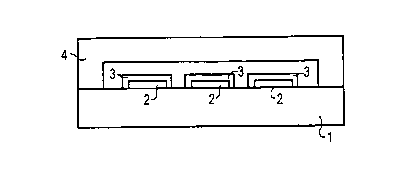
In an electronic component, especially an SW component with a conductive
structure (2) on a substrate (1) and and encapsulation (4) enclosing them on
the substrate (1), at least the conductive structures (2) are covered by a gas-
diffusion-preventing or inert protective layer (3).


French Abstract

L'invention concerne un composant électronique, notamment un composant à ondes de surface, comportant des structures conductrices (2) situées sur un substrat (1) et une encapsulation (4) enfermant lesdites structures. Sur le substrat (1) au moins les structures conductrices (2) sont recouvertes d'une couche de protection (3) empêchant la diffusion de gaz ou d'une couche inerte.

Claims

Note: Claims are shown in the official language in which they were submitted.


Patent claims:
1. A method for producing an electronic component, in
particular a component operating with surface acoustic waves
- SAW component -, having electrically conductive structures (2)
which are provided on a surface of a substrate (1), and having
encapsulation (4) which is applied on the substrate (1) and
seals the conductive structures (2), at least the conductive
structures being covered with a protective layer (3),
characterized in that a protective layer (3) which constricts
gas diffusion is produced on the conductive structures (2)
electrochemically or by ion bombardment.
2. The method as claimed in claim 1, characterized in that an
additional protective layer (5) is applied to the substrate (1)
and to the protective layer (3) which covers the conductive
structures (2) - apart from connecting surfaces (7) - pads - for
the conductive structures (2).
3. The method as claimed in claim 1, characterized in that a
further protective layer (6) which provides protection against
environmental influences is applied to the encapsulation (4).
4. The method as claimed in claims 1 to 3, characterized in
that a layer composed of an inorganic material from the group of
oxides, nitrides, carbides or oxynitrides is produced as the
protective layer (3).
5. The method as claimed in one of claims 1 to 3, characterized
in that a protective layer (5, 6) composed of an organic polymer
is applied to the protective layer (3) which covers the
conductive structures (2) and/or to the encapsulation (4).
6. The method as claimed in claim 1, characterized in that
structures which contain Al, Al+Si or Al+Ta are applied as the
electrically conductive structures (2).
7. The method as claimed in claim 1, characterized in that

- 6 -
oxides which are produced electrochemically are stabilized by
plasma treatment and/or UV irradiation.
8. The method as claimed in one of claims 1 and 7,
characterized in that reactive groups are saturated with
metal-organic compounds.
9. The method as claimed in claim 8, characterized in that
silanes are used as metal-organic compounds.
10. The method as claimed in claim 1 and one of claims 2, 4 to
9, characterized in that a further layer formation or layer
removal is carried out in order to finely adjust the thickness
of the protective layers (3, 5).

Description

Note: Descriptions are shown in the official language in which they were submitted.


- CA 02241083 1998-06-19
FILE, 1~1 IN TH~ AMENDE~
GR 95 P 2261 P ~ T TRANSLATION
Method for producing an electronic component, in particular a
component operating with surface acoustic waves - SAW
component -
The present invention relates to a method for producing anelectronic component, in particular a component operating with
surface acoustic waves - SAW component - as claimed in the
descriptive part of patent claim 1.
The prior international application WO 95/30276 discloses
encapsulation for electronic components, in particular for SAW
components, in which component structures which are applied to a
substrate are sealed by a cap which, in regions of the component
structures, has recesses which accommodate them. Such a cap is
used to protect the component structures, which in the case of
SAW components, are essentially composed of electrically
conductive structures on a piezoelectric substrate, against
environmental influences as far as possible. This applies in
particular to the encapsulation materials quoted in the said
prior patent application. However, protection is no longer
provided against gas diffusions, that is to say primarily
against water vapor diffusion, or against attacks by specific
chemical substances. In the case of some materials, the
encapsulation behaves virtually as if it were not there with
respect to water vapor diffusion. In consequence, the frequency
stability of the components can no longer be guaranteed both as
a result of water vapor diffusion and as a result of chemical
substances.
US-A-4,617,487 discloses an SAW component having a cap which is,
for example, nickel-coated for the purpose of sealing and
corrosion resistance, and which is seated in a hermetically
sealed manner on a mounting plate for the SAW component. In this
case, the entire active component structure is covered by a
closed TA pentoxide or silicone-nitride layer for protection
against possible short circuits caused by elements fragmenting
off, for example the nickel coating.
Amended sheet

CA 02241083 1998-06-19
GR 95 P 2261 P - 2 -
The present invention is based on the object of specifying, for
electronic components which are encapsulated in accordance with
the teaching of the prior patent application mentioned above, a
method which contributes to effective protection of the
components against environmental influences in the form of gas
diffusions, in particular water vapor diffusion, as well as
other chemical substances.
This object is achieved according to the invention, in the case
of an electronic component of the type mentioned initially, by a
method as claimed in the features of the descriptive part of
patent claim 1.
Developments of the invention are the subject matter of the
dependent claims.
The method according to the invention will be explained in more
detail in the following text with reference to exemplary
embodiments which are illustrated in the figures of the drawing,
in which:
Figure 1 shows a schematic illustration of an SAW component
having protection against gas diffusions, this protection being
produced using the method according to the invention;
Figure 2 shows, in the representation according to Figure 1, a
further measure according to the invention for protection
against gas diffusions;
Figure 3 shows a plan view and schematic illustration of a
detail of the SAW component according to Figure 2 that has been
treated in accordance with the invention.
The SAW component which is produced in parts using the method
according to the invention, and as is shown in Figures 1 to 3,
is in principle formed by a piezoelectric substrate 1 on which
electrically conductive structures 2, for example electrode
fingers of an interdigital converter, resonator or reflector,
Amended sheet

CA 02241083 1998-06-19
GR 95 P 2261 P - 3 -
are provided. The structures may in this case lnclude Al, Al+Sior Al+Ta. As has already been disclosed in the prior patent
application mentioned initially, the electrically conductive
structures 2 on the substrate 1 are sealed by encapsulation 4.
In order to protect these structures 2 against gas diffusions,
in particular against water vapor diffusion and chemical
substances, they are covered by a protective layer 3 which
constricts gas diffusion and, according to the invention, is
produced on the conductive structure 2 electrochemically (anodic
oxidation) or by ion bombardment.
In a development of the invention, the protective layer 3 may in
this case be, for example, a layer which is produced from an
inorganic material from the group of oxides, nitrides, carbides
or oxynitrides.
In the case of electrochemically produced oxides, stabilization
may be carried out in this case by plasma treatment and/or W
irradiation.
According to a further refinement of the invention it is
possible - as is illustrated in Figure 2 - to apply in addition
a further protective layer 5 which in turn covers the protective
layers 3 and the substrate 1. The materials already described
above are suitable, among others, for this protective layer 5.
This protective layer covers the substrate 1 and the conductive
structures 2 which are covered by the protective layers 3, with
the exception of connecting surfaces 7, that is to say so-called
pads, as is illustrated schematically in Figure 3, in which the
protective layer 3 is not shown, for reasons of clarity.
In addition to the already described protective layers 3 and 5,
a protective layer 6 can be applied to the encapsulation 4, this
protective layer 6 being illustrated by dashed lines in Fig. 2
and limiting gas diffusions even further.
The materials already mentioned above are also suitable for the
protective layer 6. Organic polymers are likewise suitable
Amended sheet

CA 02241083 1998-06-19
GR 95 P 2261 P - 4 -
materials for the protective layers 5 and 6.
In order to make the protective layers 3, 5 and, possibly, 6
absorption-constricting in addition, they can also be saturated
S with metal-organic compounds, for example silanes.
Finally, fine adjusting of the layer thickness of the protective
layers 3 and 5, and thus of the filter characteristics, can be
carried out by further layer formation or layer removal.
Amended sheet

Representative Drawing
A single figure which represents the drawing illustrating the invention.
Administrative Status

2024-08-01:As part of the Next Generation Patents (NGP) transition, the Canadian Patents Database (CPD) now contains a more detailed Event History, which replicates the Event Log of our new back-office solution.

Please note that "Inactive:" events refers to events no longer in use in our new back-office solution.

For a clearer understanding of the status of the application/patent presented on this page, the site Disclaimer , as well as the definitions for Patent , Event History , Maintenance Fee  and Payment History  should be consulted.

Event History

Description Date
Inactive: IPC from MCD 2006-03-12
Application Not Reinstated by Deadline 2004-12-16
Time Limit for Reversal Expired 2004-12-16
Deemed Abandoned - Failure to Respond to Maintenance Fee Notice 2003-12-16
Amendment Received - Voluntary Amendment 2002-07-16
Letter Sent 2001-12-12
Inactive: Adhoc Request Documented 2001-12-11
Request for Examination Received 2001-11-08
Inactive: Single transfer 2001-11-08
All Requirements for Examination Determined Compliant 2001-11-08
Request for Examination Requirements Determined Compliant 2001-11-08
Inactive: IPC assigned 1998-09-15
Classification Modified 1998-09-15
Inactive: IPC assigned 1998-09-15
Inactive: First IPC assigned 1998-09-15
Inactive: Notice - National entry - No RFE 1998-09-09
Application Received - PCT 1998-08-27
Application Published (Open to Public Inspection) 1997-07-03

Abandonment History

Abandonment Date Reason Reinstatement Date
2003-12-16

Maintenance Fee

The last payment was received on 2002-12-02

Note : If the full payment has not been received on or before the date indicated, a further fee may be required which may be one of the following

  • the reinstatement fee;
  • the late payment fee; or
  • additional fee to reverse deemed expiry.

Patent fees are adjusted on the 1st of January every year. The amounts above are the current amounts if received by December 31 of the current year.
Please refer to the CIPO Patent Fees web page to see all current fee amounts.

Fee History

Fee Type Anniversary Year Due Date Paid Date
Registration of a document 1998-06-19
Basic national fee - standard 1998-06-19
MF (application, 2nd anniv.) - standard 02 1998-12-16 1998-11-16
MF (application, 3rd anniv.) - standard 03 1999-12-16 1999-11-15
MF (application, 4th anniv.) - standard 04 2000-12-18 2000-11-09
Request for examination - standard 2001-11-08
MF (application, 5th anniv.) - standard 05 2001-12-17 2001-12-05
MF (application, 6th anniv.) - standard 06 2002-12-16 2002-12-02
Owners on Record

Note: Records showing the ownership history in alphabetical order.

Current Owners on Record
SIEMENS MATSUSHITA COMPONENTS GMBH & CO. KG
Past Owners on Record
ALOIS STELZL
HANS KRUGER
JURGEN MACHUI
WOLFGANG PAHL
Past Owners that do not appear in the "Owners on Record" listing will appear in other documentation within the application.
Documents

To view selected files, please enter reCAPTCHA code :


To view images, click a link in the Document Description column. To download the documents, select one or more checkboxes in the first column and then click the "Download Selected in PDF format (Zip Archive)" or the "Download Selected as Single PDF" button.

List of published and non-published patent-specific documents on the CPD .

If you have any difficulty accessing content, you can call the Client Service Centre at 1-866-997-1936 or send them an e-mail at CIPO Client Service Centre.


Document
Description 
Date
(yyyy-mm-dd) 
Number of pages   Size of Image (KB) 
Representative drawing 1998-09-16 1 2
Description 1998-06-18 4 157
Abstract 1998-06-18 1 13
Claims 1998-06-18 2 62
Drawings 1998-06-18 1 10
Reminder of maintenance fee due 1998-09-07 1 115
Notice of National Entry 1998-09-08 1 209
Courtesy - Certificate of registration (related document(s)) 1998-09-08 1 140
Reminder - Request for Examination 2001-08-19 1 129
Acknowledgement of Request for Examination 2001-12-11 1 179
Courtesy - Abandonment Letter (Maintenance Fee) 2004-02-09 1 176
International preliminary examination report 1998-06-17 21 792