Sélection de la langue

Search

Sommaire du brevet 2241083 

Énoncé de désistement de responsabilité concernant l'information provenant de tiers

Une partie des informations de ce site Web a été fournie par des sources externes. Le gouvernement du Canada n'assume aucune responsabilité concernant la précision, l'actualité ou la fiabilité des informations fournies par les sources externes. Les utilisateurs qui désirent employer cette information devraient consulter directement la source des informations. Le contenu fourni par les sources externes n'est pas assujetti aux exigences sur les langues officielles, la protection des renseignements personnels et l'accessibilité.

Disponibilité de l'Abrégé et des Revendications

L'apparition de différences dans le texte et l'image des Revendications et de l'Abrégé dépend du moment auquel le document est publié. Les textes des Revendications et de l'Abrégé sont affichés :

  • lorsque la demande peut être examinée par le public;
  • lorsque le brevet est émis (délivrance).
(12) Demande de brevet: (11) CA 2241083
(54) Titre français: COMPOSANT ELECTRONIQUE, NOTAMMENT COMPOSANT FONCTIONNANT A L'AIDE D'ONDES DE SURFACE ACOUSTIQUES (COMPOSANT A ONDES DE SURFACE)
(54) Titre anglais: METHOD FOR PRODUCING AN ELECTRONIC COMPONENT IN PARTICULAR A COMPONENT OPERATING WITH SUFACE ACOUSTIC WAVES-SAW COMPONENT-
Statut: Réputée abandonnée et au-delà du délai pour le rétablissement - en attente de la réponse à l’avis de communication rejetée
Données bibliographiques
(51) Classification internationale des brevets (CIB):
  • H03H 9/05 (2006.01)
  • H03H 3/08 (2006.01)
  • H03H 9/02 (2006.01)
  • H03H 9/64 (2006.01)
(72) Inventeurs :
  • PAHL, WOLFGANG (Allemagne)
  • STELZL, ALOIS (Allemagne)
  • KRUGER, HANS (Allemagne)
  • MACHUI, JURGEN (Allemagne)
(73) Titulaires :
  • SIEMENS MATSUSHITA COMPONENTS GMBH & CO. KG
(71) Demandeurs :
  • SIEMENS MATSUSHITA COMPONENTS GMBH & CO. KG (Allemagne)
(74) Agent: SMART & BIGGAR LP
(74) Co-agent:
(45) Délivré:
(86) Date de dépôt PCT: 1996-12-16
(87) Mise à la disponibilité du public: 1997-07-03
Requête d'examen: 2001-11-08
Licence disponible: S.O.
Cédé au domaine public: S.O.
(25) Langue des documents déposés: Anglais

Traité de coopération en matière de brevets (PCT): Oui
(86) Numéro de la demande PCT: PCT/DE1996/002410
(87) Numéro de publication internationale PCT: WO 1997023951
(85) Entrée nationale: 1998-06-19

(30) Données de priorité de la demande:
Numéro de la demande Pays / territoire Date
195 48 051.1 (Allemagne) 1995-12-21

Abrégés

Abrégé français

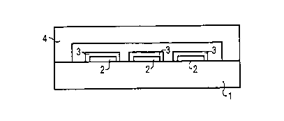
L'invention concerne un composant électronique, notamment un composant à ondes de surface, comportant des structures conductrices (2) situées sur un substrat (1) et une encapsulation (4) enfermant lesdites structures. Sur le substrat (1) au moins les structures conductrices (2) sont recouvertes d'une couche de protection (3) empêchant la diffusion de gaz ou d'une couche inerte.


Abrégé anglais


In an electronic component, especially an SW component with a conductive
structure (2) on a substrate (1) and and encapsulation (4) enclosing them on
the substrate (1), at least the conductive structures (2) are covered by a gas-
diffusion-preventing or inert protective layer (3).

Revendications

Note : Les revendications sont présentées dans la langue officielle dans laquelle elles ont été soumises.


Patent claims:
1. A method for producing an electronic component, in
particular a component operating with surface acoustic waves
- SAW component -, having electrically conductive structures (2)
which are provided on a surface of a substrate (1), and having
encapsulation (4) which is applied on the substrate (1) and
seals the conductive structures (2), at least the conductive
structures being covered with a protective layer (3),
characterized in that a protective layer (3) which constricts
gas diffusion is produced on the conductive structures (2)
electrochemically or by ion bombardment.
2. The method as claimed in claim 1, characterized in that an
additional protective layer (5) is applied to the substrate (1)
and to the protective layer (3) which covers the conductive
structures (2) - apart from connecting surfaces (7) - pads - for
the conductive structures (2).
3. The method as claimed in claim 1, characterized in that a
further protective layer (6) which provides protection against
environmental influences is applied to the encapsulation (4).
4. The method as claimed in claims 1 to 3, characterized in
that a layer composed of an inorganic material from the group of
oxides, nitrides, carbides or oxynitrides is produced as the
protective layer (3).
5. The method as claimed in one of claims 1 to 3, characterized
in that a protective layer (5, 6) composed of an organic polymer
is applied to the protective layer (3) which covers the
conductive structures (2) and/or to the encapsulation (4).
6. The method as claimed in claim 1, characterized in that
structures which contain Al, Al+Si or Al+Ta are applied as the
electrically conductive structures (2).
7. The method as claimed in claim 1, characterized in that

- 6 -
oxides which are produced electrochemically are stabilized by
plasma treatment and/or UV irradiation.
8. The method as claimed in one of claims 1 and 7,
characterized in that reactive groups are saturated with
metal-organic compounds.
9. The method as claimed in claim 8, characterized in that
silanes are used as metal-organic compounds.
10. The method as claimed in claim 1 and one of claims 2, 4 to
9, characterized in that a further layer formation or layer
removal is carried out in order to finely adjust the thickness
of the protective layers (3, 5).

Description

Note : Les descriptions sont présentées dans la langue officielle dans laquelle elles ont été soumises.


- CA 02241083 1998-06-19
FILE, 1~1 IN TH~ AMENDE~
GR 95 P 2261 P ~ T TRANSLATION
Method for producing an electronic component, in particular a
component operating with surface acoustic waves - SAW
component -
The present invention relates to a method for producing anelectronic component, in particular a component operating with
surface acoustic waves - SAW component - as claimed in the
descriptive part of patent claim 1.
The prior international application WO 95/30276 discloses
encapsulation for electronic components, in particular for SAW
components, in which component structures which are applied to a
substrate are sealed by a cap which, in regions of the component
structures, has recesses which accommodate them. Such a cap is
used to protect the component structures, which in the case of
SAW components, are essentially composed of electrically
conductive structures on a piezoelectric substrate, against
environmental influences as far as possible. This applies in
particular to the encapsulation materials quoted in the said
prior patent application. However, protection is no longer
provided against gas diffusions, that is to say primarily
against water vapor diffusion, or against attacks by specific
chemical substances. In the case of some materials, the
encapsulation behaves virtually as if it were not there with
respect to water vapor diffusion. In consequence, the frequency
stability of the components can no longer be guaranteed both as
a result of water vapor diffusion and as a result of chemical
substances.
US-A-4,617,487 discloses an SAW component having a cap which is,
for example, nickel-coated for the purpose of sealing and
corrosion resistance, and which is seated in a hermetically
sealed manner on a mounting plate for the SAW component. In this
case, the entire active component structure is covered by a
closed TA pentoxide or silicone-nitride layer for protection
against possible short circuits caused by elements fragmenting
off, for example the nickel coating.
Amended sheet

CA 02241083 1998-06-19
GR 95 P 2261 P - 2 -
The present invention is based on the object of specifying, for
electronic components which are encapsulated in accordance with
the teaching of the prior patent application mentioned above, a
method which contributes to effective protection of the
components against environmental influences in the form of gas
diffusions, in particular water vapor diffusion, as well as
other chemical substances.
This object is achieved according to the invention, in the case
of an electronic component of the type mentioned initially, by a
method as claimed in the features of the descriptive part of
patent claim 1.
Developments of the invention are the subject matter of the
dependent claims.
The method according to the invention will be explained in more
detail in the following text with reference to exemplary
embodiments which are illustrated in the figures of the drawing,
in which:
Figure 1 shows a schematic illustration of an SAW component
having protection against gas diffusions, this protection being
produced using the method according to the invention;
Figure 2 shows, in the representation according to Figure 1, a
further measure according to the invention for protection
against gas diffusions;
Figure 3 shows a plan view and schematic illustration of a
detail of the SAW component according to Figure 2 that has been
treated in accordance with the invention.
The SAW component which is produced in parts using the method
according to the invention, and as is shown in Figures 1 to 3,
is in principle formed by a piezoelectric substrate 1 on which
electrically conductive structures 2, for example electrode
fingers of an interdigital converter, resonator or reflector,
Amended sheet

CA 02241083 1998-06-19
GR 95 P 2261 P - 3 -
are provided. The structures may in this case lnclude Al, Al+Sior Al+Ta. As has already been disclosed in the prior patent
application mentioned initially, the electrically conductive
structures 2 on the substrate 1 are sealed by encapsulation 4.
In order to protect these structures 2 against gas diffusions,
in particular against water vapor diffusion and chemical
substances, they are covered by a protective layer 3 which
constricts gas diffusion and, according to the invention, is
produced on the conductive structure 2 electrochemically (anodic
oxidation) or by ion bombardment.
In a development of the invention, the protective layer 3 may in
this case be, for example, a layer which is produced from an
inorganic material from the group of oxides, nitrides, carbides
or oxynitrides.
In the case of electrochemically produced oxides, stabilization
may be carried out in this case by plasma treatment and/or W
irradiation.
According to a further refinement of the invention it is
possible - as is illustrated in Figure 2 - to apply in addition
a further protective layer 5 which in turn covers the protective
layers 3 and the substrate 1. The materials already described
above are suitable, among others, for this protective layer 5.
This protective layer covers the substrate 1 and the conductive
structures 2 which are covered by the protective layers 3, with
the exception of connecting surfaces 7, that is to say so-called
pads, as is illustrated schematically in Figure 3, in which the
protective layer 3 is not shown, for reasons of clarity.
In addition to the already described protective layers 3 and 5,
a protective layer 6 can be applied to the encapsulation 4, this
protective layer 6 being illustrated by dashed lines in Fig. 2
and limiting gas diffusions even further.
The materials already mentioned above are also suitable for the
protective layer 6. Organic polymers are likewise suitable
Amended sheet

CA 02241083 1998-06-19
GR 95 P 2261 P - 4 -
materials for the protective layers 5 and 6.
In order to make the protective layers 3, 5 and, possibly, 6
absorption-constricting in addition, they can also be saturated
S with metal-organic compounds, for example silanes.
Finally, fine adjusting of the layer thickness of the protective
layers 3 and 5, and thus of the filter characteristics, can be
carried out by further layer formation or layer removal.
Amended sheet

Dessin représentatif
Une figure unique qui représente un dessin illustrant l'invention.
États administratifs

2024-08-01 : Dans le cadre de la transition vers les Brevets de nouvelle génération (BNG), la base de données sur les brevets canadiens (BDBC) contient désormais un Historique d'événement plus détaillé, qui reproduit le Journal des événements de notre nouvelle solution interne.

Veuillez noter que les événements débutant par « Inactive : » se réfèrent à des événements qui ne sont plus utilisés dans notre nouvelle solution interne.

Pour une meilleure compréhension de l'état de la demande ou brevet qui figure sur cette page, la rubrique Mise en garde , et les descriptions de Brevet , Historique d'événement , Taxes périodiques et Historique des paiements devraient être consultées.

Historique d'événement

Description Date
Inactive : CIB de MCD 2006-03-12
Demande non rétablie avant l'échéance 2004-12-16
Le délai pour l'annulation est expiré 2004-12-16
Réputée abandonnée - omission de répondre à un avis sur les taxes pour le maintien en état 2003-12-16
Modification reçue - modification volontaire 2002-07-16
Lettre envoyée 2001-12-12
Inactive : Demande ad hoc documentée 2001-12-11
Requête d'examen reçue 2001-11-08
Inactive : Transfert individuel 2001-11-08
Toutes les exigences pour l'examen - jugée conforme 2001-11-08
Exigences pour une requête d'examen - jugée conforme 2001-11-08
Inactive : CIB attribuée 1998-09-15
Symbole de classement modifié 1998-09-15
Inactive : CIB attribuée 1998-09-15
Inactive : CIB en 1re position 1998-09-15
Inactive : Notice - Entrée phase nat. - Pas de RE 1998-09-09
Demande reçue - PCT 1998-08-27
Demande publiée (accessible au public) 1997-07-03

Historique d'abandonnement

Date d'abandonnement Raison Date de rétablissement
2003-12-16

Taxes périodiques

Le dernier paiement a été reçu le 2002-12-02

Avis : Si le paiement en totalité n'a pas été reçu au plus tard à la date indiquée, une taxe supplémentaire peut être imposée, soit une des taxes suivantes :

  • taxe de rétablissement ;
  • taxe pour paiement en souffrance ; ou
  • taxe additionnelle pour le renversement d'une péremption réputée.

Veuillez vous référer à la page web des taxes sur les brevets de l'OPIC pour voir tous les montants actuels des taxes.

Historique des taxes

Type de taxes Anniversaire Échéance Date payée
Enregistrement d'un document 1998-06-19
Taxe nationale de base - générale 1998-06-19
TM (demande, 2e anniv.) - générale 02 1998-12-16 1998-11-16
TM (demande, 3e anniv.) - générale 03 1999-12-16 1999-11-15
TM (demande, 4e anniv.) - générale 04 2000-12-18 2000-11-09
Requête d'examen - générale 2001-11-08
TM (demande, 5e anniv.) - générale 05 2001-12-17 2001-12-05
TM (demande, 6e anniv.) - générale 06 2002-12-16 2002-12-02
Titulaires au dossier

Les titulaires actuels et antérieures au dossier sont affichés en ordre alphabétique.

Titulaires actuels au dossier
SIEMENS MATSUSHITA COMPONENTS GMBH & CO. KG
Titulaires antérieures au dossier
ALOIS STELZL
HANS KRUGER
JURGEN MACHUI
WOLFGANG PAHL
Les propriétaires antérieurs qui ne figurent pas dans la liste des « Propriétaires au dossier » apparaîtront dans d'autres documents au dossier.
Documents

Pour visionner les fichiers sélectionnés, entrer le code reCAPTCHA :


Pour visualiser une image, cliquer sur un lien dans la colonne description du document. Pour télécharger l'image (les images), cliquer l'une ou plusieurs cases à cocher dans la première colonne et ensuite cliquer sur le bouton "Télécharger sélection en format PDF (archive Zip)" ou le bouton "Télécharger sélection (en un fichier PDF fusionné)".

Liste des documents de brevet publiés et non publiés sur la BDBC .

Si vous avez des difficultés à accéder au contenu, veuillez communiquer avec le Centre de services à la clientèle au 1-866-997-1936, ou envoyer un courriel au Centre de service à la clientèle de l'OPIC.


Description du
Document 
Date
(aaaa-mm-jj) 
Nombre de pages   Taille de l'image (Ko) 
Dessin représentatif 1998-09-17 1 2
Description 1998-06-19 4 157
Abrégé 1998-06-19 1 13
Revendications 1998-06-19 2 62
Dessins 1998-06-19 1 10
Page couverture 1998-09-17 1 35
Rappel de taxe de maintien due 1998-09-08 1 115
Avis d'entree dans la phase nationale 1998-09-09 1 209
Courtoisie - Certificat d'enregistrement (document(s) connexe(s)) 1998-09-09 1 140
Rappel - requête d'examen 2001-08-20 1 129
Accusé de réception de la requête d'examen 2001-12-12 1 179
Courtoisie - Lettre d'abandon (taxe de maintien en état) 2004-02-10 1 176
Rapport d'examen préliminaire international 1998-06-18 21 792