Note: Descriptions are shown in the official language in which they were submitted.
CA 02241106 1998-06-19
W O 97/25829 PCT~US96/19919
System and Method for Photonic
Facility and Line Protection Switching
Background of the Invention
Field of ~he Invention
The present invention relates generally to the reliability and restoration of
optical tr~n~mi~ion systems, and more specifically to a system and method
permitting the optimization of a number of spare components in an optical
tr~n~mic~ion system using wavelength division multiplexing (WDM).
Rela~ed Art
Optical networks that include a plurality of optical tr~ncmi~cion lines or
links perrnit high bandwidth data c~ llul~ications~ and may be used in telephoneand other data net~,vork systems. High speed data can be modulated on light
waves which are transmitted through the optical network. Further bandwidth
improvement can be achieved by mocl~ ting different electrical data signals on
distinct light wave carriers having di~el~lll frequencies. This technique is known
as wavelength division multiplexing (WDM~. Optical systems using WDM
require optical tran~ iLL~l~ and receivers that operate at different light wave
frequencies. The optical tr~n~mi~ion line, connecting an optical tr~n~mitter andreceiver, can propagate many light wave signals of different frequencies
~imlllt~neously.
Thus, fiber optic comrnunications lin~s, especially WDM communication
links, carry vast amounts of information arnong distant sites to accomplish data,
voice and image connectivity over a large geographical area. Optical
tr~n~mi~ion lines, ll~ r~ and receivers, however, are prone to failure. The
failure of such links can have a substantial economic and practical impact on
CA 02241106 1998-06-19
W O 97/25829 PCTAJS96/19gl9
-2-
network users and network service providers. Therefore, in 11esi~ning
cornmunications networks, special measures are practiced to assure utmost
reliability of network components and survivability in the event of link failuredue to physical fiber darnage or optical component failure. A common approach
to ensure resiliency to fiber cuts is the use of a spare fiber that normally does not
carry traffic but may be used as a back-up should a "working" fiber fail. To
minimi7.~ the chance that the spare fiber experiences the same fate that disabled
the working fiber, the spare fiber is usually routed along a completely different
physical path. Creating and m~i"~ g such idle spare capacity is costly.
0 Because of the expense and the non-revenue usage, what is needed is a restorative
network design where the deployment of spare facilities and spare fiber links iskept to a minimllm
Summary of the Invention
In accordance with the present invention, there is provided a system and
method of photonic facility and line protection switching using frequency or
wavelength translation in facilitating a fault-tolerant optical network. In the
present invention, the optical network comprises working and protect facilities,working and protect optical tr~n~mi~ion lines, optical space division switches
(SDSs), and digital cross-connect switches (DCCSs). A working or protect
facility is comprised of one or more optical tr~n~mit~ers and/or receivers.
Wavelength or frequency translation capability is provided using tunable protecttransmitters, tunable protect receivers, and frequency translators coupled to
optical space division switches.
The SDS is an optical cross-connect switch facilitating routing of optical
signals. It is desirable to use a miniml-m number of ports on an SDS to reduce
SDS cost and complexity. The present invention uses SDSs with a small number
CA 02241106 1998-06-19
W O 97~5829 PCT~US96~9919
of ports. The DCCS is an electrical cross-connect switch facilitating the routing
of electrical signals.
The optical tr~n.~mitters, receivers, and tr~n.~mi~ion lines have different
expected reliabilities. The use of both SDSs and DCCSs permits an optical
network to be optimally configured with an a~plo~l;ate amount of working and
protect facilities and optical tr~nsmi.ssion lines. Depending upon the expected
transmitter and tr~n~mi.~ion line failure rates, an optical system can be
configured in accordance with the present invention to include an ~ upl;ate
number of protect optical tr~nsm;ffers independent of the number of protect
optical tr~n~mi~sion lines. It is an advantage of the present invention that theratio of working facilities to protect facilities is independent of the ratio ofworking optical trz~n~mi~ion lines to protect optical tr~n.~mi~sion lines.
In the event of a component failure in the optical network, the SDSs and
DCC~s can respectively re-route optical and electrical signals to col~lpc;llsate for
a failed component such as an optical tr~n~mit~r, receiver, or tr~n.~mi.~sion line.
The present invention comprises a protect, or spare, facility or optical
tr~n.~mix~ion line with which to replace a corresponding failed component.
Because the network can replace a failed component with a corresponding
protect, or spare, component, the optical network can continue functioning
despite the failure.
According to a further aspect of the present invention, wavelength
fr~n~l~ti~n is provided to o~hlli~ facility and line protection ~wilcl~ g. Protect
facilities include a tunable optical lldll~llliU~. and a tunable optical receiver. A
frequency tr~n~l~tor, also called a wavelength tr~n~ r, ;s optically coupled to
an SDS for tr~n~l~fing the frequency or wavelength of optical signals.
Further features and advantages of the present invention, as well as the
3 structure and operation of various embo~iment~ of the present invention, are
described in detail below with reference to the accolll~lying drawings.
CA 02241106 1998-06-19
W O 97/25829 PCT~US96/19919
Brief Description of the Drnwings
The accompanying drawings, ~hhich are incorporated herein and form part
of the specification, illustrate the parent invention and, together with the
description, further serve to explain the principles of the invention and to enable
a person skilled in the art to make and use the invention.
FIG. 1 is a block diagram of a first embodiment of an optical net~,vork
with photonic facility and line protection according to the present invention.
~IG. 2 is a flow chart of the operation of the first embodiment of an
optical network with photonic facility and line protection.
FIG. 3 is a block diagram of a second embodiment of an optical network
with fre~uency or wavelength translators according to the present invention.
FIG. 4 is a flow chart of the operation of the second embodiment of an
optical network with frequency translators.
FIG. 5 is a block diagram of a third embodiment of an optical network
using frequency or wavelength translators according to the present invention.
FIG. 6 is a flowchart of the operation of the third embodiment when the
number of failed working fibers exceeds the nurnber of protect fibers.
The present invention is described with reference to the acconlpalLyillg
drawings. In the drawings, like reference numbers intlir~te identical or
functionally similar elements. Additionally, the left-most digit(s) of a reference
number identifies the drawing in which the reference number first appears.
Detailed Description of the Preferred Embodiments
The present invention is directed towards facilitating a fault tolerant
optical network. This goal is achieved with photonic facility and line protection
CA 02241106 1998-06-19
W O 97/25829 PCTAJS96/19919
--5--
using protect, or spare, optical components, such as facilities and optical
tr~n~mi~ion lines. The topology of the optical network permits use of space
division switches (SDSs) with few ports, reducing SDS cost and complexity.
Further advantages are realized by providing frequency or wavelength translationcapability through lunable protect transmitters, tunable protect receivers, and/or
frequency translators coupled to optical space-division switches.
Tunable Fa~il;fi~
The present invention takes advantage of wavelength division
multiplexing (WDM) to add another dimension to restorative design approaches.
Previously, a given fiber was associated with a single optical transmitter and asingle optical receiver. When one of these devices failed, the restorative action
was the same as with a fiber failure, that is, electronically switching the traffic
onto a completely different transmitter/fiber/receiver link. But with wavelengthdivision multiplexing, several transmitters feed a single fiber.
The present invention handles single ~ l~iu~l or single receiver failures
in a WDM configuration by electronically and optically switching a reserve,
protect tunable facility to replace a corresponding failed facility. The use of a
tunable receiver or tr~n~milter in conjunction with a bridgeable optical switch
(SDS) yields the unexpected advantage of allowing facility operation ratios to be
designed independent of the line protect ratios. For example, the optical domainswitching can allow a single tunable transmitter to serve as a backup facility for
nine different transmitters operating along three working fibers. The same
configuration can provide a three-to-one line protect ratio. These protect ratios
can be set totally independently of one another. This design freedom is an
important advantage because tr~n~mitt~qr failures occur at dirr~ L rates than fiber
failures.
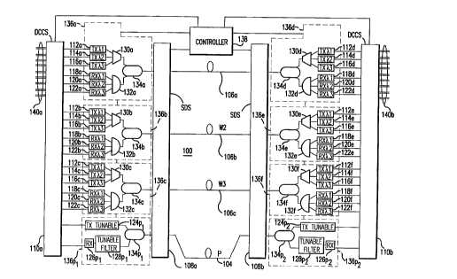
~ FIG. 1 illustrates one embodiment of an optical network 100 with a
protect optical tr~n~mi~sion line 104 and protect tunable facilities 136pl and
CA 02241106 1998-06-19
W O 97/25829 PCT~US96/19919
136p2. The present invention contemplates that the optical network 100 may
include more than one protect optical trsln~mi~sion line lQ4 or two protcct
facilities 136pl and 136p2. In a preferred embodiment, the protect facilities 136p~
and 136p2 comprise protect optical tr~n.~i" ,i l l~ 124pl and 124p2, protect optical
receivers 126p~ and 126p2, tunable filters 128pl and 128p2, and a three-port
coupler device 134p, and 134P2-
To perrnit frequency, or wavelength, agility, the carrier frequency of the
optical transmitters 112a-f, 114a-f, 116a-f is made variable by using a tunable
source, such as a tunable laser, or a fixed source coupled to a frequency translator.
The frequency translator may be an optical mixer. Hence, the optical transmittermay be a tunable optical tr~n~mitt~r. Also, the optical receivers 118a-f, 120a-f,
122a-f, must be tunable so that they can detect the correspondingly broadcast
wavelength. The tunable optical receiver may be implemented with a tunable
filter 128pl and 128p2 as illustrated in FIG. 1 for the protect receivers 126pl and
126p2.
The optical network 100 comprises two digital cross-connect switches
(DCCSs) 110a,b for switching, routing, multiplexing, and demultiplexing
electlical signals into higher or lower bit-rates. Electrical signals, which may be
in a STS- 1 or DS-3 format compliant with SONET standards or any other data
format and bit rate, are coupled into and out of ports 140a,b of DCCSs 110a,b.
The DCCSs 110a,b are coupled to facilities 136a-f for converting electrical
signals to optical signals and vice-versa. In the preferred embodiment, the
facilities 136a-f include optical L~ lllillel~ 112a-f, 114a-f, 116a-f, optical
receivers 118a-f, 120a-f, 122a-f, combiners 130a-f, splitters 132a-f, and three port
coupler devices 134a-f.
Optical network 100 further includes a pair of space division switches
~SDSs) 108a,b, also called optical cross-connect switches, and working optical t
tr~n~mi~ion lines 106a-c. SDS 108a, 108b can be any type of multi-port optical
cross-connect switch. In principle for a N X N SDS any number of ports, e.g. N
= l, 2, 4, 8, 16, 40, 72, 128, or 256, can be switched. Any type of optical switch
CA 02241106 1998-06-19
W O 97/25829 PCTAJS96fI9919
can be used depending upon the available technology. See, e.g., the integrated
lithiUm niobate directional-coupler type switches (lisc~lssed by Waynant, R. et al.,
Eds., Electro-Optics Handbook, McGraw-Hill, Inc. U.S.A. (1994), chapter 26,
and especially page 26.34 (incorporated herein by reference). Other types of
suitable optical switching technology include switches based on a therrno-optic
effect in polymer waveguides or silica glass, semiconductor amplification, piezomovement, and integrated indium phosphide.
In addition, while a single SDS 108a and SDS 108b is shown
schematically for clarity, multiple discrete switches and couplers can be used to
perform equivalent mllltiI-le-port optical switching. For example, a set of discrete
1 X 2 or 2 X 2 optical switches can used to switch individual signals along optical
paths between cross-connected ports. Y-couplers and directional couplers can
also be used.
The embodiment illustrated in FIG. 1 is specifically implemented in an
optical network 100 using wavelength division multiplexing (WDM). Hence,
certain components of the optical network 100 are bro~-lh~nc~, including ~e three
port devices 134a-f, 134pl and 134p2, combiners 130a-f, 130p, and 130p2, and
splitters 132a-f, 132p, and 132p2. The protect transmitter 124p~ and 124p~ has atunable carrier frequency and the protect optical receiver 126pl and 126p2 can
selectively detect light wave signals of varying carrier frequency by eh~n~ng the
p~sb~n~l frequency of a tunable filter 128p~ and 128p2 coupled to the protect
optical receiver 126pl and 126p~. In the p~c;r~ d embodiment, the tunable filters
128p~ and 128p2 are implemPnte-1 with Fabry-Perot filters. However, alternative
embodiments of the tunable filters 128p, and 128p2 can be used.
The electrical signals are routed by the DCCSs 11 Oa,b to or from optical
tr~n~miltPrs 112a-f, 114a-f, 116a-f or receivers 118a-f, 120a-f, 122a-f,
respectively, as ~lesiP~n~tp~ by a controller 138. Distinct electrical signals
entering optical network 100 are modulated onto light wave carriers having
different frequencies (e.g., frequencies corresponding to wavelengths A" il2, and
;~3) by the optical tr~n~mitters 112a-f, 114a-f, 116a-~ In a preferred embodiment,
CA 02241106 1998-06-19
W O 97n5829 PCTrUS96/19919
the optical tr~n~mitters 112a-f, 114a-f, 116a-f are modulated lasers, such as,
directly modulated semiconductor laser diodes, or externally modulated lasers.
Other types of optical transmitters and modulators can be used. For the sake of
clarity, only working facilities 136a and 136d are described in detail.
In one working facility 136a, the outputs ofthe optical tr~nsmitters 112a,
114a, 116a having (lirre~ output carrier frequencies, i.e., wavelengths ~, to A.3,
are unified in a combiner 130a which is then connected to a three port device
134a. The three port device 134a permits bidirectional light wave signals to be
coupled into and out of separate ports. In the pl~er~ lled embodiment, the threeport device 134a may be comI-ri~ed of a directional coupler, such as those made
with fused optical fibers. Other types of three port devices 134a made of known
fiber optic components can be used. The three port device 134a is connected to
the SDS 108a.
Under normal conditions, SDS 108a routes the combination of mo~ t~rl
light wave signals having different carrier frequencies into the optical
tr~n~mi~ion line 106a. In the preferred embodiment, the optical tr~n~mi~sion
line 106a includes bidirectional optical fibers, line repeaters, and/or amplifiers.
However, the optical tr~n~mi~sion line 106a can comprise only unidirectional
optical fibers and amplifiers. AltPrn~tively, the optical tr~n~mi~ion line 106a
could comprise a long-haul, single-mode optical fiber exclusively. The other endof the optical tr~n~mi c~ion line 106a is coupled to another SDS 108b which routes
the light wave signals to another working facility 136d and its corresponding
three port device 134d during normal operation.
The light wave signals then propagate from the three port device 134d to
2~ a splitter 132d. In a pl~rel,~ed embodiment, the splitter 132d includes a WDM
multiplexer (not shown) which has frequency selective outputs corresponding to
the carrier fre~uencies comprising the light wave signal. The WDM multiplexer
is typically formed by an optical grating that spatially separates light of different
wavelengths.
CA 02241106 1998-06-19
W O 97/25829 PCTAJS96/I9919
Alternatively, the splitter 132d may comprise a n-way power divider.
Wavelength selectivity can be attained with the n-way power divider by insertingfilters between the n-way power dividers and the optical receivers 118d, 120d,
122d. However, filters are not needed if the optical receivers 118d, 120d, 122d
are frequency selective.
Each output of the splitter 132d is coupled to an optical receiver 118d,
120d, 122d. Inthepreferredembodiment,theopticalreceivers 118d, 120d, 122d
are standard optical detectors. ~lt~rn~tive optical receiver 118d, 120d, 122d
embodiments can be used. The optical receiver 118d, 120d, 122d demodulates
an electrical signal from the light wave signal of the corresponding carrier
frequency. The electrical signal is then coupled through a second DCCS 11 Ob to
one of its ports 140b back to the electrical domain.
A controller 138 is connected to components, such as the optical
trz~n~mitt~rs 112, 114, 116 and receivers 118, 120, 122, in the optical network
100. The controller 138 senses whether the optical network components are
functioning properly. In a ~.~r~lled embodiment, the controller 138 is a
processor and detects loss of signal and/or other types of optical faults.
Alternatively, the controller 138 can comprise a plurality of distributed processors
that are coordinated by a co--, lnu- ' 'cations link (not shown). If a component fails,
the controller 138 re-routes the signals passing through the failed component toa protect, or spare, component, utili7in~ the switching capabilities of the SDSs108a,b and DCCSs llOa,b. Spare components include a protect optical
tr~n.~mi~ion line 104, a protect optical receiver 126pl and 126p2 with a tunablefilter 128pl and 128p2, and/or a protect optical tr~n~mitt~-r 124p, and 124p2.
FIG. 2 illustrates a flow chart of exemplary operation of the fault tolerant
nature of the optical network 100. The functionality described below is
implemented by controller 138. When optical network 100 comrnences
operation, or alternatively when the optical network first detects a component
fault, (step 202), the controller 138 evaluates whether any of the optical
tr~n~mi~ion lines 106a-c have failed (step 204). One way for the optical network
CA 02241106 1998-06-19
W O 97/25829 PCTAUS96119919
- 10-
100 to ~l~tPrmine optical tr~n~mi~ion line 106a-c failure is for the controller 138
to monitor the lack of reception of light wave signals by all optical receivers
118a-f, 12Qa-f, 122a-f connected to a specif1c optical tr~n~mi~ion line 106a-c.
If the conkoller 138 determines that àn optical tr~n~mi~ion line 106a-c
has failed, the controller 138 comm~n(1~ a corresponding SDS 108a,b to re-route
the optical signals to an available protect, or spare, optical trzln~mi~ion line 104
(step 206). While aprotect optical tr~n~mi~sion line 104 is ~ltili7~-1 it is generally
unavailable for further use.
Upon replacing a failed optical 1rAn~mi.~ion line or if none was found, the
controller 138 evaluates whether any optical transmitters 112a-f, 114a-f, 116a-fhave failed (step 208). If the controller 138 determines an optical transmitter
112a-f, 114a-f, 116a-fhasfailed,thecontroller 138comm~ntlcthecorresponding
DCCS 110a,b to re-route the electrical signals from the failed optical transmitter
to a protect, or spare, optical ~ 124p, and 124p2 (step 210). At about the
same time, the protect optical tr~n~mht~r 124p, and 124p2 is tuned to the
wavelength corresponding to the failed optical transmitter as directed by
controller 138. The re-routed electrical signal is modulated on a light wave
carrier by the protect optical tr~n~mitt~r 124pl and 124p~. The resulting
modulated light wave signal is then coupled through some of the same
components, including the working optical tr~n.~mi~sion line 106a-c and the
optical receiver 118a-f, 120a-f, 122a-f, that the original light wave signal hadpropagated through before the optical tr~n~mitter 112a-f, 114a-f, 116a-f failure.
Finally, upon replacing a failed optical transmitter, or if none was found,
thecontroller 138will~1et~rmineifanyopticalreceivers 118a-f, 120a-f, 122a-f
have failed (step 212). If the controller 138 determine~ an optical receiver 118a-f,
120a-f, 122a-f has failed, then the controller 138 comm~n~l~ the corresponding
SDS 108a,b to re-route the light wave signal from the failed optical receiver toa protect, or spare, optical receiver 126p, and 126p2 (step 214).
One example of how the controller 138 may determine that an optical
receiver 118a-f, 120a-f, 122a-fhas failed is now described. The optical receiver
CA 02241106 1998-06-19
W O 97/25829 PCT~US96~g91
118a-f, 120a-f, 122a-f presents to controller 138 a signal indicating that optical
receiver 118a-f, 120a-f, 122a-f has detected a light wave signal. If the opticalreceiver 118a-f, 120a-f, 122a-f does not present such a signal, and the controller
138 determines that there is no corresponding optical tr~n~mi.~.cion ~ine 106a-cS failure, then the controller 138 ~,vill conclude that the optical receiver 118a-f,
120a-f, 122a-f has failed.
At about the same time the controller 138 comm~n-l~ the SDS 108a,b to
re-route the light wave signal, the controller 138 regulates the protect opticalreceiver 126p, and 126p2 operating frequency by setting the p~c~bS-ncl of the
corresponding tunable filter 128p, and 128p2. The detected electrical signal is re-
routed by a DCCS 110a,b to the same port 140a,b that the demodulated electrical
signal exited before the optical receiver 118a-f, 120a-f, 122a-f failure.
If operation of the controller 138 is halted, the aforementioned process
will be stopped (step 218). Otherwise the process will repeat itself, again
analyzing if an optical tr~n~mi~ion line 106a-c failure has occurred (step 204).Note, however, that some of the steps described above could be
implementecl in another order or in parallel. Such an implementsltion would be
~ent to one skilled in the art.
Frequency Translators
According to a further advantage of the present invention, optical network
capacity is ,"~;"I~;,.ed in the event that a working optical tr~n.~mi~.sion line fails
and no protect optical tr~n.cmi~ion line is available to replace it. In such an
event, the present invention transfers the signals of the failed working opticaltr~n.~mi.c~ion line to another working optical tr~n~mi~ion line. Fre~uency
translators are provided to permit these additional restored carrier signals to
co-exist with the normal carrier signals being transmitted on the other working
optical tr~n~mi~ion line.
CA 02241106 1998-06-l9
W O 97/25829 PCT~US96/19919
-12- -
A second embodiment of the present invention is illustrated in FIG. 3.
The optical network 300 in FIG. 3 has two frequency translators 302a,b opticallycoupled to ports in the two space division switches 108a,b. The frequency
translators 302a,b are coupled to the controlier 138. The frequency translators
302a,b permit a composite set of carrier signals (~l to ~) to be adjusted to
another set of wavelengths (~4 to A,6). ~or example, the SDS 108a routes the
signals that previously would have traveled on the failed working optical
tr~n~mi~sion line to frequency translator 302a coupled to the SDS 108a. The
carrier frequencies ~, to i~,3 of the signals are then modified in the frequencytranslator 302a to ;L4 to ;~6. The signals are re-routed by the SDS 108a to another
working optical tr~n~mi~sion line 106a-c.
At least two frequency translators for accomplishing frequency or
wavelength translation are known. See, e.g., the articles by Zhou et al., "Four-Wave Mixing Conversion Efficiency in Semiconductor Traveling-Wave
Arnplifiers Measured to 65nm of Wavelength Shift", IEEE Photonics Technology
~,etters, Vol. 6, No. 8 (August 1994~; and Riazat et al., "Optical Wavelength
Shifting by Traveling-Wave Electrooptic Modulation", IEEE Photonics
Technology Letters, Vol . 5, No. 9 (September 1993) (each of which is
incorporated herein in its entirety by reference). One technique involves four-
wave mixing through a non-linear semiconductor optical amplifier as described
by Zhou et al. This technique is analogous to the heterodyning (mixing) of high
frequency electrical signals commonly done in radio equipment. The second
technique uses traveling-wave electrooptic modulation wherein microwaves and
optical signals travel through a substrate together. As described by Riazat et al.,
the microwaves produce a refractive index gradient in the substrate that travelswith, and alters the wavelength of, the passing optical signal. One or more
frequency translators 302a,b can be coupled to the optical network 100.
FIG. 4 illustrates a flow chart of exemplary operation of the optical
network 300 using one or more frequency translators 302a,b. The functionality
CA 0224ll06 l998-06-l9
W O 97~5829 PCTMS96t~ggr9
-13-
described below is implemented by controller 13 8 which starts fault detection at
step 402 when optical network 300 commences operation.
In step 404, the controller 138 determines whether any optical
tr~n~mi~ion lines have failed. If the controiler 138 det~rmines that no optical
tr~n~mi~ion lines 106a-c have failed, the controller 138 may continue to search
for optical tr~n~mi~ion line 106a-c faults (step 416) or cease searching (step
418). However, if the controller 138 ~l~tf~rmint?s that an optical tr~n~mi~ion line
106a-c has failed, the controller 138 will next deterrnine if a protect optical
tr~n.~mi~ion line 104 is available for use. If a protect optical tr~n~mi~ion line
104 is available for use, the controller 138 will re-route the signals from the failed
optical tr~n~mi~ion line 106a,b through the protect optical L~ .lli.s.~iion line 104.
However, if no protect optical tr~n~mi~ m line is available or if none was
irnplemented in the optical network 300, the controller 138 will re-route optical
data signals from the failed optical tr~n~mi~.~ion line 106a-c through each SDS
108a,b to one or more frequency translators 302a,b and over an available workingtr~n.~mi.~.cion line 106a-c (step 412). For example, in the frequency translator302a, the signals will be shifted from an initial set of carrier frequencies to
another set of optical carrier frequencies, allowing the signals from any of thetr~n~mitt~.rs 112a-c, 114a-c, 116a-c, or 124pl to be tr~n~mitted through the SDS108a over a functioning working or protect optical trAn ~mi ~ion line 106a-c, 104
with other signals at different carrier frequencies without interference (step
412). These tr~n~l~te~1 optical signals can then be routed through SDS 108b for
detection as the tr~n~1~ted wavelength or frequency by any aL)~ iately tuned
receiver 118d-f, 120d-f, 122d-f, or 126p2.
Alternatively, the controller 138 can route the translated s;gnals to the
other frequency translator 302b so that the signals are frequency shifted back to
their initial frequency (or another frequency) so that the signals can be ~lçtectç~l
by the optical receivers 118d-f, 120d-f, 122d-f, or 126p2.
Alternatively, signals can be routed from the second SDS 108a,b to
tunable receivers which are adjusted by the controller 138 to detect the signals
CA 02241106 1998-06-l9
W O 97~5829 PCT~US96/19919
-14-
having the shifted carrier frequencies. The optical network 100 may then choose
to continue searching for failed optical kz~n~mi~sion lines (step 416) or stop its
analysis (step 418~.
Some of the steps described above could be implemented in another order
or in parallel. Such an implementation would be ~palent to one skilled in the
art.
A third component of the present invention is illustrated in FIG. 5 in an
optical network 500. For clarity, only network elements for communication in
one tr~n~mi~ n direction from electrical inputs 140a to output electrical outputs
140b are shown. Only active ports A to I in SDS 108a and ports A to G in SDS
108b are shown. Other ports could be provisioned as needed.
One wavelength or frequency translator 502 is optically coupled to the
optical space-division switch 108a. The wavelength translator 502 accepts a set
of multiplexed optical carrier signals at wavelengths, e.g., ~I to ;l3, and outputs
a wavelength-shifted set of optical carrier signals, e.g., ;l4 to A,6, that exhibit the
same relative separation and modulation characteristics. A protect receiver
facility 510 is coupled between SDS 108b and DCCS 11 Ob for transducing carrier
signals. A splitting element 520 passes carrier signals received from the SDS
108b to three tunable receivers 521. For example, splitting element 520 can be
one or more optical components, such as, beam splitters, filters, and/or gratings
for splitting input carriers into three separate signals. The tunable receivers 521 -
523 are then tuned to detect a particular wavelength within a respective separated
signal. During normal operation, three tunable receivers 521-523 are tuned to
detect an initial set of wavelengths ~I to ~3. During restoration, the three tunable
receivers 521-523 are tuned to detect the shifted-set of wavelengths A,4 to A,6
generated by the wavelength translator 502.
Network 50û provides frequency agility which allows restoration of
network capacity even when no protect fiber is available or the number of
working fiber failures exceeds the number of protect fiber provided. The
restoration operation of network 500 in the event two working fibers 106a and
CA 02241106 1998-06-19
W O 97/25829 PCT~US96~I9919
- 15-
106b are damaged will be described with respect to FIG. 6. The restoration
operation is caIried out through controller 138 (not shown) which is connected
to SDS 108a, 108b, wavelength translator 502, working and protect facilities
(k~n~mit~ers 112-116a-candreceivers 118-122d-e, 521-523~, andDCCS 110a,
11 Ob, as described earlier with respect to FIGs. 1 and 3.
~DSs 108a and 108b are switched to re-route traffic from the working
flber 106a to protect fiber 104 by connecting ports A and H in SDS 108a and
ports D and E in SDS 108b (step 602~. SDS 108b is switched to connect port C
to ports F and G (step 604). DC~CS 11 Ob is switched so that carrier signals from
tr~n~ 112c-116c are received at receivers 118e-122e (step 606).
Tunable receivers 521-523 are tuned to the shifted set of wavelengths ;1,4
to i~6 (step 608). SDS 108a switches to connect ports B and I so that a composite
set of signals from the tr~n~...i(~. j 112b-116b enters wavelength tr~n~l~tQr 502
(step 610). The wavelength translator 502 is set and/or adjusted to shift the set
of wavelengths from the initial waveleng~s ~l to ;~3 to the shifted-set of
wavelengths 14 to ~6 (step 612). Finally, SDS 108a switches to connect ports D
and G so as to superimpose the carrier signals having the shifted-set of
wavelengths onto normal traffic carried by working fiber 106c for detection by
the tuned receivers 521-523 (step 614).
It should be understood that embodiments of the present invention can be
implemented in h~dw~, software or a combination thereof. In such
embodiment, the various components and steps would be implemented in
.lw~ and/or software to perform the functions of the present invention. Any
presently available or future developed computer software language and/or
hal-lw~ components can be employed in such embodiments of the present
invention. In particular, the flow chart discussed above can be especially useful
for creating the software embodiments.
While various embodiments of the present invention have been described
above, it should be ~m~1~r~od that they have been presented by way of example
only, and not limitation. Thus, the breadth and scope of the present invention
CA 02241106 1998-06-19
W O 97/25829 PCTAUS96/19919
-16-
should not be limited by any of the above-described exemplary embo~liment.c, butshould be defined only in accordance with the following claims and their
equivalents.