Note: Descriptions are shown in the official language in which they were submitted.
CA 0224111~ 1998-06-19
WO 97n401~ PCT/US96/20434
PATENT APPLICATION
ELECTROLUMINESCENT FILAMENT
This application is a continuation-in-part of pending U.S. application
No. 08/578,887, filed December 22~ 1995, which is inco,yol~ted herein by
reference.
BACKGROUND
The present invention relates to electroluminescent filaments ("EL
filaments"). More specifically, the present invention relates to EL fi1~rnPnt~,
portions of which may be individual]y ilh1min~t~1
EL filaments have been known generally in the art; however, few
S have been produced beyond a test scale and the conventional filarnents have
had a series of problems, including low reliability and low light intensity. In
addition, the conventional EL filarnents lack sufficient flexibility to be made
into one-, two-, and three-~lim~ncional light emitting objects using textile
fabrication technologies such as knitting, weaving, braiding, etc., that use rawmaterials in fil~m~ont~ry form.
Conventionally, EL fil~ment~ include a central solid core conductor
coated with a l1-min~scent material and an outer electrode that is made of
either a single conductor wound around the core or a transparent con~ cting
film coated onto the lI.minçscing layer. Since the conventional fil~n~ent~
1~ include only a single outer electrode or ~ ls~Jarclll coated electrode, it is not
possible to energize individual portions of the conventional fil~m~nt~ This is
a drawback in applications which re4uire different portions of the fil~nlPnt to
be energized at different times; for example, applications that require
~nim~tçrl visual effects. The conventional filaments that contain only one
outer electrode have the additional drawback that if the outer electrode is
CA 0224111~ 1998-06-19
WO 97/24015 PCT/US96120434
broken anywhere along the fi~ ent~ the whole filament ceases lurninescing
This makes the conventional filaments easily susceptible to damage.
There therefore exists a need for a reliable, flexible EL fil~ment that
is capable of emitting high light intensity when energized and which may be
made into articles or incorporated into articles using textile fabrication
techniques. There is also a need for an EL fil~m~nt, only portions of which
may be energized at any one time. Moreover, there is a need for an EL
filament which does not fail completely when only a part of the filament is
darnaged.
SUMMA}~Y
The present invention addresses the above needs by providing an EL
fil~ment that includes a core conductor, a l.-min~scing layer surrounding the
core conductor, and a braided outer electrode either embedded in the
hlminf scing layer or surrounding the l--min~qscing layer. In one embodiment,
the core conductor is a multi-strand conductor. In a preferred emborlim~ nt
the core conductor is a multi-stranded conductor, the braided outer electrode
covers about 50% of the surface of the Illminescing layer, and the
Illmin~oscing layer includes an activated zinc sulfide encapsulated phosphor.
In another embodiment of the invention, the braided outer electrode
includes a plurality of individually addressable electrodes. If the individual
electrodes are in.~ ted from one another, they may be individually energized
thereby ill--min~ting only a portion of the EL fil~m~nt. One embodiment of
the present invention that achieves the above includes a core conductor, a
2~ h~min~scing layer at least partially surrounding the core conductor and two
or more individually addressable electrodes disposed around the core
conductor. In this embodiment of the invention, the individually addressable
electrodes are in~ ted from one another; additionally, the individually
addressable electrodes may be braided together to forrn an outer electrode,
-2 -
CA 02241115 1998-06-19
PCT/US96/20434
wo 97/24015
and may be embedded in the luminescing layer or disposed surrounding the
luminescing layer.
To facilitate addressing the individual electrodes in the previous
embodiment, the EL filament may also include a coupler for connecting the
S individual electrodes to the external power source. The coupler connects the
closely spaced, fragile individual electrodes to more easily accessible, thickermore robust wires that may then be ~ rh~d to the power circuit. The
coupler may connect the individually addressable electrodes to t~,vo or more
power inputs. Generally, a coupler includes robust, durable co.~;ls
connected to the more fragile individually addressable electrodes. These
contacts are for connecting to the external power source and for supplying
power to the individually addressable electrodes.
BRIEF DESCRIPTION OF THE DRAWINGS
The invention will be better understood with rer~,e.lce to the ~tt~chP~l
figures in which:
Figure 1 shows a cross-sectional view of one embodiment of an
electrolllminescent fil~m~nt according to the present invention;
Figure 2 shows a cross-sectional view of one embodiment of an
electroll-minescçnt filament according to the present invention;
Figure 3 shows a longitudinal elevation of one embodiment of an
electrolnminescent fil~m-ont according to the present invention;
Figure 4 shows a longitudinal elevation of one embodiment of an
electrol~ scel-t filament according to the present invention;
Figure 5 shows a longitudinal elevation of one embodiment of an
electrolnmin~-ccçnt fil~m~nt according to the present invention;
Figure 6 shows a cross-sectional view of one embodiment of an
electrolllminescent fil~m~nt according to the invention;
Figure 7 shows a cross-sectional view of one embodiment of an
electroll.min~scent filament according to the present invention;
-3-
CA 0224111~ 1998-06-19
WO 97/2401~ PCT/US96/20434
Figure 8 shows a cross-sectional view of one embodiment of an
electrol--minescent filament according to the present invention;
Figure 9 shows a cross-sectional view of one embodiment of an
electrolurninescent filament according to the present invention;
Figure 10 shows a cross-sectional view of one embodiment of an
electrol~-minescPnt filament according to the present invention;
Figure 11 shows a perspective side view of one embodiment of an
electrohlmin~o.uent filament according to the present invention;
Figure 12 shows a series of wave forms that may be used for driving
the electrolnmin~oscent fil~mçnt of Figure 11;
Figure 13 shows a pc,~eelive top view of one embodiment of a
coupler according to the present invention connected to arl electroh-min~oscent
filament according to the present invention;
Figure 14A shows a cross-sectional view of one embodiment of a
coupler according to the present invention conn~ct~d to an electrohlmin~ scent
filament according to the present invention;
Figure 14B shows a top plan view of the coupler of Figure 14A; and
Figure 15 shows a perspective top view of one embodiment of a
coupler according to the present invention connecte~l to an electrolllmin~scent
filarnent according to the present invention.
DETAILED DESCRIPTION
We have found that when an EL fi1~mP.nt is fabricated using a multi-
strand core conductor and a braided outer electrode the resulting fil~ment is
flexible enough to be used in textile fabrication technologies, and also has a
light emission intensity and reliability that will allow it to be used
commercially. This combination of flexibility, reliability, and bri~htn~.c
enab}es the EL filarnents of the present invention to be used in a variety of
applications including illllrnin~tecl logos, illllmin~ted materials for use in night
clothing, safety clothing, color change cloth, outlining objects for safety,
-4 -
CA 0224111~ 1998-06-19
WO 97/24015 PCT/US96120434
ilhlmin~ted embroidery, and illl.min~ted needlepoint. In addition, the EL
filaments of the present invention may be braided over a non-conducting core
such as a cotton fiber. This will produce a thicker more robust light emitting
fiber which can be woven into belts etc, or which may be used to make
ill~-min~te~l nets which may be used, for example, in basketball, tennis, etc.
Generally, an electrolllmin~sce.lt fil~m~nt accordi.lg to the present
invention includes a core cor-fhlctor, a h.minescin layer surrounding the core
conductor, and an outer electrode surrounding the core conductor and
in.~nlst~cl from the core conductor. By "surrounding" we mean that element
A surrounds element B if element A at least partially covers the surface of
element B. As used here, element A does not have to be in contact with
element B to surround it; moreover~ element A does not have to cover the
entire surface of element B to surround it. For example, as used here, a
helical shaped wire wound around but not touching a core, "surrounds" the
I ~ core.
The electrolnrninesc~nt filament may optionally include a first
insulation layer surrounding the core conductor and a second insulation layer
surrounding the l-lrninescing layer. In one embodiment of the invention, the
outer electrode may surround the h-min~sçing layer. In an alternative
embodiment, the outer electrode may be embedded in the lllminescing layer.
If the filament includes a second insulation layer the outer electrode may be
embedded in this insulation layer. To provide strength while m~int~inine
flexibility, the core may be multi-stranded and the outer electrode braided.
As described in detail below, additional braided layers may be added to
2~ improve strength, cut-through resiet~nce, etc.
Generally, an electroh~ sc~l.t fii~m~nt produces light in response to
an alternating or pulsed DC current source connected across the core
conductor and outer electrode. The core conductor and the outer electrode
can be connected across a voltage source in order to produce light as desired.
It is possible to use more than one voltage source with a single filament.
-5-
CA 0224111~ 1998-06-19
WO 97124015 PCT/~JS96t20434
This may be the case if more than one outer electrode is present in the
fil~m~nt (see below) or if a multi-stranded core conductor is used.
The electrol~lminescent filaments of the present invention may be used
to fabricate shapes that emit light when they are connected to and energized
by the a~ op.iate electrical power supply. The filaments of the present
invention are flexible enough to be knitted, woven, braided, etc. using textile
fabrication technologies that use raw materials in filamentary form. Using
these technologies, the filaments of the present invention may be used to
make all sorts of one, two, and three tlimencional light emitting objects.
Exarnples of such objects include clothing, works of art, molded parts, and
inforrnational displays. In clothing. for example, electroluminescent threads
can be used to embroider logos, de~ignc, or other accents.
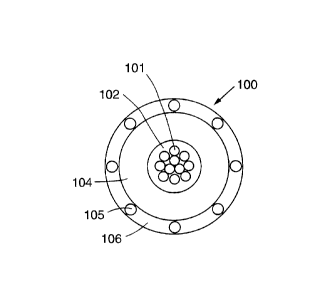
Figure 1 shows one embodiment of an electroluminescent filament
according to the present invention. The fil~m.ont 100 includes a core
conductor 101, a first in~ ting layer 102, a h.min~scing layer 104, an outer
electrode 105, and a second in~ tin~ layer 106.
Core Conductor
The core conductor 101 is a conductor or semi-conductor, and may be
of a single or multiple filamentary metallic or carbonaceous material, other
electrically conducting or semi-conducting materials or combinations thereof.
The core conductor 101 may be solid or porous. The cross-sectional shape of
the core conductor 101 may be circular, flat, or any other acceptable
geometry. Preferably, the core conductor 101 is a multiple-strand
2~ configuration of conducting filaments bec~ se bundles of fine fil~mPnt~ are
more flexible than a solid individual filament. The multiple-strand
configuration adds strength and flexibility to the fil~mPnt.
Accordingly, in a preferred embodiment of the filament, the core
conductor is a multi-strand core conductor. These multi-strand core
conductors may be in a parallel, coiled, twisted, braided, or another
-6 -
CA 02241115 1998-06-19
WO 97124015 PCT/US96120434
acceptable configuration or arrangement. The number of strands, their
individual di~m~tçrs, composition, the method of p~-~4ing and/or number of
twists may be of any combination.
A particularly preferred core conductor material is a 19-strand bundle
S of stainless steel conductor fil~m~nss. Each strand (filament) is about 50gauge (roughly equivalent to about 0.001 inch dia.). Each strand bundle has
a fluorinated ethylene propylene (FEP) in.cul~tion layer about 0.002 inch
thick, with an overall wire conductor outside ~ metPr of about 0.012 inch
~insulation inclusive). Such a core cnn~ll.r.tor is available from Baird
Industries (Hohokus, NJ).
First Insulation Layer
Figure l shows an embodiment of the invention in which the filament
or filaments of the core conductor are surrounded by a first insulation layer
102 of insulating material. While the first in.~ ting layer 102 is not required
to practice the invention, its presence is preferred. The first in~lllating layer
102 serves to reduce the probability of shorts between the core conductor and
an outer electrode, thus increasing reliability.
In the embodiment shown in Figure l, the first insulation layer 10~
surrounds the core conductor. In the case of a multi-strand core conductor,
each strand may be individually surrounded by an optional first insulation
layer. An additional insulation layer may also surround the entire bundle of
individually surrounded strands.
Luminescing Layer
Figure l shows an embodiment of the invention which includes a
luminescing layer 104 surrounding the insulation layer or layers. The
lurninescing layer 104 preferably comprises "phosphor." Phosphor is a term
that has evolved to mean any material that will give off light when placed in
an electric field. The light may be of a variety of wavelengths. The
-7-
CA 0224111~ 1998-06-19
WO 97124015 PCTJUS96/20434
lllminf scing layer 104 may be deposited as a continuous or interrupted
coating on the outer surface of the core conductor?s insulation layer. When
the lnminPscing layer 104 is deposited as an interrupted coating, the result
may a striped or b~n~e~l light producing product. If there is a plurality of
individually in~ul~ted strands, the l-lrninesçing layer may be coated on each
strand or disposed between the in~ tecl strands.
Alternatively, the phosphor may be compounded directly into the first
insulation layer and applied by extrusion or another process. In this
embodiment, the first insulation layer and the luminescing layer are the same
1 0 layer.
Typically, phosphor is comprised of copper and/or m~n~nese
activated zinc-sulfide particles. In a preferred embodiment, each phosphor
particle is e~r~ps~ ted to improve service life. The phosphor may be either
neat or in the form of a phosphor powder/resin composite. Suitable resins
include cyanoethyl starch or cyanoethyl cellulose, supplied as Acrylosan~ or
Acrylocel~ by TEL Systems of Troy, Ml. Other resins, possessinp. a high
dielectric strength, may be used in the composite matrix material.
A particularly preferred material for use in the ll~min~scing layer 104
is the phosphor-based powder known as EL phosphor, available as EL-70
from Osram Sylvania Inc. (Towanda, PA). A preferred formulation for the
composite is 20% resin/80% phosphor by total weight of the con-posilion.
However, other weight ratios may be used.
Other phosphors are available which emit different wavelengths of
radiation, and combinations of phosphors may be used.
2~ The luminescing layer 104 may be deposited in any number of ways,
such as: thermoplastic or thermoset proce~ing, electrostatic deposition,
fluidized powder bed, solvent casting, printing, spray-on application or other
acceptable methods.
Another method for ~n~,hing the Illrnin~scing layer 104 to the first
insulation layer, or to other suitable layers, if suitable for use with the
-8-
CA 02241115 1998-06-19
WO g7/2401~ PCT/US96120434
materials in question, is to soften the first insulation layer 102, or other
suitable layers with heat, or a solvent or other method and then to imbed the
phosphor material into the first insulation layer 102, or other suitable layers.
Outer Electrode
Figure 1 shows an embodiment of the invention in which an outer
electrode 105 surrounds the hlminPscing layer 104. In another embodiment
of the invention, the outer electrode 105 may be applied before or
simultaneously with the Illminescing layer 104. The outer electrode 105
comprises an electrically conductive or semi-conductive material, and
preferably, the outer electrode has a braided fil~rn~nt~Ty skucture. By
"braided fil~ y structure" we mean a plurality of individual electrodes
that are braided together. The individual electrodes that make up the braided
outer electrode may be coated or uncoated. One advantage of an EL fil~m~nt
that includes a braided outer electrode is that if any of the individual
electrodes that make up the braided sL~ e are damaged the filament will
continue to l~lmin~sce; only if all of the electrodes in the braided electrode
are damaged will the fil~nent cease lurr inescing~ The fil~mPnt~ of the
present invention therefore have a built in redlln-l~n~y in the outer electrode;a feature which makes the fil~ nt~ of the present invention more durable
than conventional fil~m~nt~ that contain only one individual outer electrode.
Examples of suitable outer eleckode materials include metal, carbon, metal
coated fibers, inherently cond~lcting polymers, intrinsically conducting
polymers, compounds co..~ g indium tin oxide, and semicon-h~ctors.
Other outer electrode configurations include: p~lror~led wrap-around metallic
foils (wherein the perforations may be of any shape, i.e., circular, slot or
other); eleckically conducting knitted, woven or non-woven cloth or fa~ric;
non-woven mat material such as overlapping electrically conducting whiskers
or tinsel; any other eleckical conductor; or any combination of these
materials. The outer electrode is preferably made of a non-transparent
CA 0224111~ 1998-06-19
WO 97/24015 PCT/US96/20434
material. In this case, it is also preferred that the outer electrode is non-
continuous (e.g., braided structure, foraminous, etc.) to allow the electro-
ll~minescence generated in the llltninescent layer to be emitted through the
outer electrode.
Second Insulation Layer
Figure I shows an embodiment of the invention which includes a
second insulation layer 106 within which the outer electrode 105 is
embedded. In an alternative embodiment the insulation layer 106 may
surround the outer electrode 105. The second insulation }ayer 106 is
preferably comprised of an optically ~ J~elll, electrically inclll~tin~
material, such as an amorphous or crystalline organic or inorganic material.
The second insulation layer 106 may be applied in liquid or other form with
a subsequent cure or other process that may result in a permanent, semi-
perrnanent, or temporary protective layer. Particularly ~)r~l.ed materials
include epoxies, silicones, urethanes, polyarnides, and mixtures thereof.
Other materials may be used to achieve desired effects. The transparent,
electrically in~ul~ting, materials may also be used in other layers.
The second in~ tion layer 106 is not required, but is desirable to
improve reliability. The second insulation layer 106 also improves the "feel"
(i.e., surface texture) of the fil~ment and rçslllting goods made from the
filament.
A silicone coating resin, such as Part No. OF113-A & -B, available
from Shin-Etsu Silicones of America (Torrance, CA), may be used for the
second insulation layer 106. The silicone resin lCE1871, available from Shin-
Etsu Silicones of America, may also be used for the second insulation layer
106.
Figure 2 shows an embodiment of the present invention that includes a
core conductor 201, surrounded by a first insulation layer 202, which is
surrounded by an interlayer 203. The interlayer 203. is surrounded by the
-10-
CA 02241 1 lF7 1998 - 06 - 19
WO 97124015 PCT/US96/20434
I--minescing layer 204, which is surrounded by a second insulation layer 206,
having embedded within it an outer electrode 205.
ln this embodiment, the l..min~scing layer 204 is attached to the
outermost surface of the first insulation layer 202 using one or more adhesion
promoting interlayers 203. Interlayers 203 may be used generally to promote
interlayer adhesion, or for other desired effects, such as modification of
dielectric field strength or improved longitudinal strain performance. To
promote adhesion to the surface of the first insulation layer, any process to
modify the surfaces plol,c.lies may be used, such as: mechanical abrasion,
chemical etching, physical embossing, laser or flame treatment, plasma or
chemical tre~tment or other processes to improve the surface plopellies.
Figure 3 shows an embodiment of the invention that includes a core
conductor 301 surrounded by a first insulation layer 302, which is surrounded
by a Illminescin~ layer 304. The Illminescing layer 304 is surrounded by a
second insulation layer 306, having ~mhe~lded within it a braided outer
electrode 305. The braided outer electrode may include three or more
individual electrodes forming a diagonal pattern. The individual electrodes
may be intertwined. The braided structure may form a wire grid. Braids
may include counter-wound individual eiectrodes having an under and over
geometry. Figure 10 shows a more detailed depiction of the over and under
geometry of a counter-wound braid 105. Braided structures add strength and
flexibility to the filament.
The braided outer electrode may be formed from several different
individual electrodes which can have the same or different gauges. The
individual electrodes can have the same or different sizes, shapes, and
compositions. In the embodiment shown, the individual electrodes are
braided over the electroll~min~scent core. Preferably, the braid covers about
50% of the electrolllminpscpnt core although more or less coverage may be,
used in specific applications.
- 1 1 -
CA 0224111~ 1998-06-19
WO 97/24015 PCT/US96120434
Figure 4 shows an embodiment of the invention that includes a core
conductor 401 surrounded by a first insulation layer 402, which is surrounded
by an interlayer 403. The interlayer 403, is surrounded by the l--min~scing
layer 404, which is surrounded by a second insulation layer 406, having
S embedded within it an electrode 40~. The interlayer 403 is preferably an
adhesion promoting interlayer, but may also serve some other purpose in
improving the operation of the filament.
Figure S shows an embodiment of the invention that includes a core
conductor ~01 surrounded by a first insulation layer 502, which is surrounded
by an h~mintoscing layer 504. The l~lrninescing layer 504 is surrounded by a
second insulation layer 506 which is surrounded by an electrode S05. The
outer electrode 505 is surrounded by an additional protective layer 506a. The
additional protective layer 506a may be of any of the materials generally
disclosed herein.
I S Figure 6 shows an embodiment of the invention that includes a
dielectric braid 607 surrounding the first insulation layer 602 and embed~l~d
in the luminescing layer 604. To form the dielectric braid 607, a dielectric
fiber is braided, spiral wlal~ed, or applied using a combination of both
geometries, onto the first insulation layer 602. The dielectric braid 607 may
also be produced by braiding, spiral wrapping, or using a combination of both
geometries~ a dielectric fiber onto the core conductor 601, such that the
dielectric braid 607 surrounds the core conductor 601. The dielectric braid
607 also surrounds the core conductor 601, or the first insulation layer 602
that surrounds the core conductor 601.
Generally, dielectric braiding may be used in any of the layers of the
invention, using dielectric fibers as described below.
The dielectric fibers forming the dielectric braids described herein
may be made of glass~ Kevlar~), polyester, acrylate, or other organic or
inorganic materials suitable for use as dielectric fibers. The Illlnin~oscing
layer(s) described herein is applied over this dielectric braid. The dielectric
-12-
CA 0224111~ 1998-06-19
WO 97/24015 PCT/US96/20434
fiber layer then acts as a coating thickness controller and may aid in adhering
the Illmin~scent layer to the core conductor.
This adhesion improvement is particularly helpful when the first
insulation layer is a low friction and/or low adhesion coating, such as a
fluoropolymer coating. Additionally, the dielectric fiber layer provides
improved resict~nce to "cutthrough" and improved axial strength because the
dielectric fiber layer will act as a strength member. The outer electrode
described herein may be then directly applied to the phosphor co~ ;..ing
dielectric fiber layer, and the second insulation layer described herein is
applied to the outer electrode.
Figure 7 shows an embodiment of the invention that includes a core
conductor 701 surrounded by a first insulation layer 702, which is surrounded
by an interlayer 703. The interlayer 703 is surrounded by a dielectric braid
707, similar to the dielectric braid 607 of Figure 6. The h.minescing layer
704 is coated over the dielectric braid 707, similar to the relationship bel~ elJ
the ll.minescing layer 604 and the dielectric braid 607 of Figure 6.
Surrounding the ll-min~ccine layer 704 is the second insulation layer 706,
having embedded within it the outer electrode 705.
Figure 8 shows an embodiment of the invention that includes a core
conductor 801 surrounded by a first insulation layer 802, which is surrounded
by a dielectric ~raid 807, similar to the dielectric braid 607 of Figure 6. The
h-rninPscing layer 804 is coated over the dielectric braid 807, similar to the
relationship between the lllmin~scing layer 604 and the dielectric braid 607 of
Figure 6. Surrounding the lurninescing layer 804 is the second insulation
layer 806, having embedded within it both the outer electrode 805 and a
second dielectric braid 808. The second dielectric braid 808 may be of the
same materials as the dielectric braid already described.
Figure 9 shows an embodiment of the invention that includes an outer
electrode 905, for example a braided wire electrode, that is applied directly
on the first insulation layer 902. In another embodiment, the outer electrode
-13-
CA 0224111~ 1998-06-19
WO 97/24015 PCT/US96/20434
905 may be applied directly on the core conductor g01, so long as they are
insulated in some way. In the embodiment shown, the entire structure is then
coated with the material of the lllminescing layer 904. The outer electrode
905 is then embedded in the luminescing layer 904. The outer electrode 905
thus applied may be combined with dielectric m~teri~l~. For example, if the
outer electrode 905 is a braided wire electrode, it may be combined so as to
be co-braided with a dielectric braid 907 directly onto either the optional first
insulation layer 902, or the core conductor 901 directly. An interlayer 903,
for example an adhesion promoting interlayer, may also be present if desired.
Additional layers or fillers may be added, or the above mentioned
layers may be modified. For example, the use of transparent colored
materials andlor translucent materials in the layers may alter the ~l~e~ of
emitted light, thereby producing different colors. Opaque materials may be
used in the layers, producing, for exarnple, a striped product. Phosphorescent
(i.e., "glow-in-the-dark"), and reflective materials may also be used. The
reflective materials may be particulates, or they might be sheet material.
Other additives may be used to correct color output and filter the
spectral emission. For example, a laser dye may be added to the phosphor
composition or coated on top of the phosphor composition or coated on top
of the phosphor coating. This material will alter the spectral emission.
Additional layers, not herein described, may be added, as long as they
result in a usable electroh....il-escellt fil~ment as would be recognized by oneof ordinary skill.
Individually Addressable F.l~ct~odes
Figure 11 shows an electrolnmin~scçnt fil~mer~t 1000 according to the
present invention that includes a braided outer electrode 1010, a Illmin~scent
layer 1020, and a core conductor 1030. The figure shows a braided outer
electrode 1010 that includes a plurality (six in the embodiment in Figure 11)
of individually addressable electrodes 1040-1045. In this embodiment, the
-14-
CA 0224111~ 1998-06-19
WO 97/24015 PCT/US96/20434
individually addressable electrodes are insulated from one another. This may
be achieved, for example, by braiding the outer electrode 1010 using
individually inc~ ted electrodes 1040-1045. This embodiment may
optionally include insulation layers, interlayers, dielectric braids, and other
layers as described above.
ln operation, the individually addressable electrodes of this
embodiment may be ''energized" individually. By "ene,~i~ed" we mean that
an AC (or pulsed DC) voltage difference is applied between an individual
electrode and the core conductor. If the individually addressable electrode
that is energized is in~ ted from the other individual electrodes, an electric
field will only be produced in the space between the energized electrode and
the core conductor. Therefore, only the phosphor in the luminescent layer
that is between the energized electrode and the core conductor will
electroll.minesce. In this way, it is possible to make only portions of the EL
filament emit light.
Figure 12 shows an example of a set of voltage waveforms that may
be used to produce a chasing light pattern in the EL filarnent of Figure 11.
In Figure 12, wave form 1050 co,l~spol1ds to the voltage applied between the
core conductor and electrode 1040, wave form 1051 corresponds to the
voltage applied between the core conductor and electrode 1041, efc. By
controlling the se~uence of excitation of each electrode individually, any
nurnber of time dependent light patterns and effects can be produced. In one
embodiment of the invention, the individual electrodes are energized in a
se~uence that is controlled using a microprocessor. The use of a
microprocessor to control multiple electrol~.minçscent lamps has been
described previously in U.S. Patent Application No. 08/698,973, filed August
16, 1996, which is incorporated herein by reference. By sequentially
energizing the braided individually addressable electrodes using waveforms
similar to those shown in Figure 12, a spiral chasing light pattern was
observed. By controlling the sequence of the individual electrodes, it will be
-15-
CA 0224111~ 1998-06-19
WO 97/24015 PCT/US96/2O434
possible to produce many different light patterns such as barber pole effects,
and moving stripes. In addition, by selectively registering colored layers with
the positions of the individual electrodes, it will be possible to make the EL
filarnent emit different colors when different individual electrodes are
S energi~d.
Figure 13 shows one embodiment of a coupler 1060 for facilitating
coupling the individually addressable electrodes to the power source. In this
embodiment, the coupler 1060 includes a separator or manifold 1070 that has
an opening 1080 to accomrnodate the EL filament 1090. The individually
addressable electrodes 1100-1103 (4 electrodes in this example) are
electrically connected to wires I 1 10-1 1 13 via contact pads 1 120-1 123. The
core conductor 1130 is also exposed to be connected to the power source.
The wires I 1 10-1 1 13 are more robust and durable than the individually
addressable electrodes 1100-1103 and these wires are connected to the power
supply circuits and microprocessor controller. The individually addressable
electrodes may be conn~cte~l to the contact pads via conventional methods;
for example, soldering.
Figures 14A and 14B shows cross-sectional and plan views of a
connector similar to that shown in Figure 13.
Figure 15 shows another embodiment of a coupler according to the
present invention. ln this embodiment the coupler 1200 includes a set of
conducting pins 1210 mounted in a sep~dtor 1220. One end 1220 of the
pins 1210 is connected to the individually addressable electrodes and the core
conductor. Again, the electrodes and the conductor may be ~ ch~d to the
pins using conventional methods such as soldering. In operation, the end
1230 of the pins not connected to the electrodes is connected to the power
supply. Generally, a coupler includes a means for connecting the fragile
individual electrodes to the external power supply. It is preferred that this
means includes durable, robust contacts connected to the individual electrodes
and for supplying power to the more fragile electrodes. In addition, the
-16-
CA 02241115 1998-06-19
WO 97/24015 PCT/US96/20434
coupler may also serve to spatially separate the individually addressable
electrodes for easy access and manipulation.
When an El fil~m~t includes individually addressable electrodes, it is
possible to remove the core electrode complete}y. In this embodiment of the
invention, a voltage difference is applied bet~,veen different individually
addressable electrodes in the outer electrode. This voltage difference
produces an electric field which causes the l~ minescent layer to emit light.
In this embodiment of the invention, the cond~lctin~ core may be absent
altogether or may be replaced by a non con~ ctinE core, which may be used
to add strength to the fil~ment. In this embodiment of the invention, it is
preferred that the outer electrode is embedded in the llnninescing layer.
CA 0224111~ 1998-06-19
WO 97124015 PCT/US96/20434
Example of an EL Filament According to the Present Invention:
A core conductor, comprised of a 19 strand bundle of 50 gauge wire,
is selected. The entire bundle has a 2 mil thick fluoropolymer insulation
coating that forrns the first insulation layer. The first insulation layer is then
S coated with a particulate composite of an 80/20% by weight phosphor powder and resin mixture.
The particulate composite is prepared as a solution/suspension by
mixing the al)plopliate ratio of phosphor powder and resin with a 50150
mixture of acetone and dimethyl~et~mide. The viscosity of the
solution/suspension may be adjusted by varying the solvent/solids ratio. To
apply the coating, the core conductor is passed through a vertically oriented
reservoir of phosphor composite, ~vith a coating die at the bonom of the
reservoir controlling the coating's thickness during the deposition process.
The solvents are removed from the wet coating as the wire passes through a
series of in-line, heated tube furnaces. The result is a solidified composite
coating con~ining the phosphor. Using a binarv blend of solvents assists the
drying process, as the two solvents evaporate at different rates due to
differences in boiling points. The fini~hecl product is a uniform, concentric
and approximately 2 mil thick phosphor coating forming the lurninescing
layer on the first insu}ation layer.
Next~ a 16-count (number of carriers) braider is used to produce a
50% coverage of I mil diameter v~ire over the l~ scing layer. This braid
forms the outer electrode.
Finally, a second coating reservoir with an apl)lopliate (li~rn~t~r sizing
die is used to apply the second insulation layer onto the wire. The coated
filament is passed through in-line tube furnaces to convert the second
insulation layer into its final form.
- I 8-