Note: Descriptions are shown in the official language in which they were submitted.
CA 02241404 1998-06-25
SPECIFICATION
TITLE OF THE INVENTION
Contact-type Image Sensor
TECHNICAL FIELD
The present invention relates to a contact-type image
sensor used in a facsimile machine, image scanner, photocopying
machine and so on.
PRIOR ART
Contact-type image sensors are commonly used for reading
characters, symbols and other forms of information recorded
on a medium such as paper. An image sensor typically comprises
an array of light emitting elements as a light source, and an
array of light receiving elements. The light emitting element
is typically a light emitting diode (LED) whereas the light
receiving element is typically a CCD. In operation, light from
the light emitting element array is directed to the information
medium. The light reflected by the medium is sensed by the light
receiving element array so that the image (information) on the
object medium can be detected by photoelectric conversion.
Conventionally, a contact-type image sensor of the above
type has an arrangement shown in Fig. 9 for example.
Specifically, a contact-type image sensor represented by
the numeral code 10 has a substrate I2 provided on a bottom
portion of a case 11. The substrate 12 has an array of image
1
CA 02241404 1998-06-25
sensor tips 12 corresponding to a reading width. The case 11
has an upper surface attached with a transparent cover glass
14. Between the cover glass 14 and the image sensor chip array
13, and aligned with a predetermined reading line L, there is
disposed a rod lens array 15 fitted to a support groove 18 formed
in the case 11. The rod lens array 15 is known as the selfoc
lens array, by which an image on the reading line L is projected
as an erected isometric image on the image sensor chip array
13.
The case 11 also includes an inclined substrate 17. The
inclined substrate 17 has a plurality of LED chips 16 as a light
source from which light is cast to an object D obliquely through
the cover glass 14 . The object D is moved by a platen P for
example while contacted to the cover glass 14.
According to the above contact-type image sensor 10, the
LED chips as the light source should be mounted on the inclined
substrate 17 instead of the substrate 12 at the bottom so that
the object D can be lighted as efficiently as possible. For
this reason, the two substrates 12, 17 must be mounted
individually, which complicates assembling of the image sensor
10. Using two kinds of substrates 12, 17 increases the number
of parts , makes an arrangement more complex, and hence increases
cost.
Theoretically, it is possible to eliminate the inclined
substrate 17 , and mount the LED chips 16 on the bottom substrate
12 together with the image sensor chip array 13. Such an
arrangement is not practical, however, because only a very small
2
CA 02241404 1998-06-25
portion of the light from the LED chips 16 can reach the object
D.
Further, with the above arrangement of the image sensor
10, the LED chips 16 are disposed at a higher position than
are the image sensor chips 13, being closer to the object D.
As a result, the light from each of the LED cannot adequately
disperse widthwise (i.e. in the longitudinal directions of the
image sensor chip array 13 ) before reaching the object D. Thus,
if a distance between adjacent pair of LED chips 16 is large,
quantity of light often becomes uneven widthwise of the object
D. This problem may be solved by increasing the number of LED
chips 16, disposing the LED chips closer to each other. However,
this solution creates a new problem of increased cost due to
the increased number of LED chips 16.
DISCLOSURE OF THE INVENTION
It is therefore an object of the present invention to
provide a contact-type image sensor having a simple
construction for easy assembly.
Another object of the present invention is to provide a
contact-type image sensor in which quantity of light does not
easily become uneven in the directions of scanning even with
a small number of light sources.
According to a first aspect of the present invention, there
is provided a contact-type image sensor comprising a common
substrate provided with a plurality of light receiving elements
and a light source, and a light guide for directing the light
3
CA 02241404 1998-06-25
from the light source obliquely toward an object.
Advantages of the above arrangement will be discussed later
in detail with reference to the accompanying drawings.
According to a preferred embodiment of the present
invention, the light guide comprises a prism. The prism
includes a first incidence surface facing the light -source,
a second incidence surface facing the light source while being
inclined at a predetermined angle relative to the first
incidence surface, at least one total reflection surface, and
an outlet surface for casting obliquely toward the object the
light reflected by the plane of total reflection surface after
incidence via the first and second incidence surfaces.
The first incidence surface of the prism is generally
parallel to the substrate whereas the second incidence surface
of the prism may be inclined relative to the substrate. Further,
both the first and second incidence surfaces of the prism may
be inclined relative to the substrate. Still further, the
prism may have the first incidence surface inclined relative
to the substrate and the second incidence surface generally
vertical to the substrate.
For improved lighting efficiency, the light coming from
the light source should be prohibited from escaping. For this
reason, the prism should be intimately fitted in a holding space
of the case. Further, the prism may have ends each provided
with a fitting block for intimately fitting in an end portion
of the mounting space of the case in order to facilitate ease
and reliability in assembly operation. Still further, the
4
CA 02241404 1998-06-25
prism should preferably have a longitudinally intermediate
portion formed with an engaging projection. This projection
engages with a recess formed in an inner side wall of the case,
prohibiting the prism from spontaneously coming out.
Generally, a plurality of LED chips are used as the light
source.
According to a second aspect of the present invention, there
is provided a contact-type image sensor comprising a case, a
glass cover provided on an upper surface of the case, a bottom
substrate mounted in a bottom surface of the case, a plurality
of light receiving elements mounted on the bottom substrate,
a plurality light emitting elements for irradiating an object
on the glass cover with light, and a rod lens array for collecting
the light reflected by the object on the glass cover onto the
light receiving elements. The light emitting elements are
mounted on the bottomsubstrate. The contact-type image sensor
further comprises a light guide provided in the case for
efficiently directing the light from the light emitting
elements to a predetermined region of the glass cover.
According to a preferred embodiment of the present
invention, the,case is formed with a holding groove for
receiving the rod lens array from above. The light guide has
ends each formed with a tab for pressing the rod lens array
from above. Further, the holding groove may be formed with a
projection for engagement with a longitudinally intermediate
portion of the rod lens array from above.
Other objects, features and advantages of the present
5
CA 02241404 1998-06-25
invention will become clearer from the detailed description
of the preferred embodiment to be made with reference to the
accompanying drawings.
RRTFF nFSC'RTPTTON OF THE I~HAWINGS
Fig. 1 is an exploded perspective view of a contact-type
image sensor according to a first embodiment of the present
invention.
Fig. 2 is a fragmentary plan view of the image sensor.
Fig. 3 is an enlarged sectional view taken along lines
III-III in Fig. 2.
Fig. 4 is an enlarged sectional view taken along lines Iv-IV
in Fig. 2.
Fig. 5 is an enlarged sectional view taken along lines V-V
in Fig. 2.
Fig. 6 is a fragmentary perspective view showing a variation
to the first embodiment, differing only in means for fixing
a cover glass to a case.
Fig. 7 is a cross-sectional view showing a contact-type
image sensor according to a second embodiment of the present
invention.
Fig. 8 is an exploded perspective view showing the image
sensor according to the second embodiment.
Fig. 9 is a cross-sectional view showing a prior art
contact-type image sensor.
6
CA 02241404 1998-06-25
BEST MODE FOR CARRYING OUT THE INVENTION
Preferred embodiments of the present invention will be
described in specific detail referring to the accompanying
drawings.
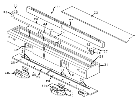
Figs. 1 through 5 show a contact-type image sensor 20
according to the present invention. The image sensor 20
comprises a long case 21 having a predetermined length and a
generally rectangular cross section. The case 21 can be molded
integrally of resin. As clearly shown in Fig. 3, the case 21
has an inner space S as a perpendicular through hole, with a
glass cover 22 sealing an upper opening, and a bottom substrate
23 sealing a bottom opening.
The bottom substrate 23 has an upper surface mounted with
an array of image sensor chips 24 along a longitudinal edge
of the surface. On the same surface of the bottom substrate
23, and along the other longitudinal edge, a plurality of LED
chips 25 are provided in a row at a predetermined interval.
According to the present embodiment, each of the LED chips 25
is a bear chip (which is not molded in a package).
The inner space S of the case 21 includes a light guide
26 made of a transparent resin for effectively directing the
light from the LED chips 25 to an object D on the glass cover
22. According to the present embodiment, as shown in Fig. 5,
the light guide 26 is a prism having a predetermined section,
including a horizontal first incidence surface 26a, an inclined
second incidence surface 26b, an inclined first total
reflection surface 26c, a vertical second total reflection
7
CA 02241404 1998-06-25
surface 26d, and an inclined outlet surface 26e. The prism may
be suitably made of a transparent resin material such as
polymethyl methacrylate (PMMA), polycarbonate and
polystyrene.
The inner space S of the case 21 further includes a rod
lens array 27 (selfoc lens array) disposed in parallel to the
light guide (prism) 26 for collecting reflected light from the
object D into an erected isometric image on the image sensor
chip array 24. The rod lens array 27 is held by a holder portion
28 which receives the rod lens array from above. The holder
portion 28 has a holding groove 29 corresponding to the plan
view shape of the rod lens array 27, and a bottom portion formed
with a slit 30 for allowing the light from the rod lens array
27 to pass through to the image sensor chip array 24.
As clearly seen in Figs. 1 and 3, the holder portion 28
has a long inner wall. A longitudinally intermediate portion
of the inner wall is formed with a pair of projections 31 for
engaging with an upper face of the rod lens array 27 so that
the rod lens array 27 will not spontaneously come up. As shown
in Fig. 3, each of the projections 31 has an appropriate height
and is formed with a tapered upper face 31a so as not to interfere
with the rod ~.ens array 27 when the rod lens array is inserted
into the holder portion 28.
The light guide 26 or the prism introduces the light from
the LED chips 25 efficiently to and around a reading line L.
The reading line L is disposed on an optical axis O of the rod
lens array 27 whereas the LED chips are disposed away from the
8
CA 02241404 2000-10-02
axis on the bottom substrates 23. The light guide 26 is fitted
in a space enclosed by an inner side wall 21a of the case 21,
a side wall 28a of the groove holder portion 28, and a bottom
wall 33. The bottom wall is formed with a window 32 faced to
the LED chips 25.
As shown in Fig. 1, the light guide 26 has a longitudinal
side face with an intermediate portion formed with a couple
of engaging projections 34. Further, as shown in Fig. 3, the
inner side wall 21a of the case 21 is formed with corresponding
engaging recesses 35 to engage with the projections 34.
As shown in Figs. 1 and 5, the light guide 26 has end portions
each formed with a fitting block 36 of a predetermined height
for fitting between the inner side wall 21a of the case and
the side wall 28a of the holder portion 28. Each of the fitting
block 36 is formed integrally with an extending tab 37 for
pressing a corresponding end portion of the rod lens array 27
from above. One of the fitting blocks 36 has a back face formed
with a projection 38 whereas the other fitting block 36 has
a back face formed with a rib 39. When each of the fitting blocks
36 is fitted between the inner wall 21a of the case and the
side wall 28a, the projection 38 and the rib 39 hold respective
fitting blocks 36 firmly by increased friction.
With the above arrangement, the contact-type image sensor
20 of the above arrangement can be assembled in the following
steps. Specifically, the rod lens array 27 is inserted from
above into the holding groove 29 of the holder portion 28 in
the case 21. In this step, each of the engaging projections
9
CA 02241404 1998-06-25
31 formed in the inner wall of the holder portion 28 engages
with the upper face of the rod lens array 27 so that the rod
lens array 27 will not spontaneously come up.
Next, the light guide 26 is fitted from above into the space
enclosed by the inner side wall 21a of the case and the side
wall 28a of the holder portion 28. In this step, each of the
engaging projections 34 formed in the light guide 26 engages
with the corresponding recess 35 of the case 21. Further, the
fitting blocks 36 are held in the space firmly by friction,
so the light guide 26 are held accurately at a predetermined
position, being prohibited from spontaneous upward rise. The
pressing tab 37 extending from each of the fitting block 36
of the light guide 26 presses from above the corresponding end
portion of the upper face of the rod lens array 27. Thus, the
rod lens array 27 is pressed at its longitudinally intermediate
portions by the engaging projections 31 and at its
longitudinally end portions by the pressing tabs 37, thus being
held stably and firmly at the predetermined position.
The glass cover 22 is fitted by bonding for example, into
the upper opening of the case 21. The bottom substrate 23 is
fitted into the .bottom opening of the case 21 and is fixed by
metal clamps 40. As shown in Figs. 1 and 4, each of the clamps
40 is a generally U-shaped piece of spring steel with each of
its leg portions 40a formed with an engaging hole 41 to engage
with a corresponding engaging projection 42 formed on
corresponding outer side faces of the case 21.
As described above, in the contact-type image sensor 20
CA 02241404 1998-06-25
according to the present embodiment, the rod lens array 27 and
the light guide 16 can be assembled by simple fitting operations
using no adhesive, separate fasteners or tools. Further, one
bottom substrate 23 includes not only the image sensor chip
array 24 but also the plurality of LED chips as light source.
This eliminates a need for a separate substrates for the LED
chips 25, reducing the number of necessary parts as a whole,
simplifying the assembly operation, and reducing the cost of
the contact-type image sensor.
Further, according to the above embodiment, the bottom
substrate 23 placed to the bottom opening of the case 21 is
held to the case by the metal clamps 40. Thus, the bottom
substrate 23 can also be fixed to the bottom face of the case
21 by a simple operation without relying upon such complicated
fixing means as bonding or screwing.
Now, the contact-type image sensor 20 with the above
arrangement operates as follows . Specifically, as shown in Fig.
4, when each of the LED chips 25 illuminates, the light from
the chips enters the light guide 26 after refracting on the
horizontal first incidence surface 26a or the inclined second
incidence surface 26b of the light guide 26. The light coming
into the light guide 26 is totally reflected by the inclined
first total reflection surface 26c or the vertical second total
reflection surface 26d. The light is refracted again on the
outlet surface 26, and then goes out of the light guide 26
obliquely. After getting out of the light guide 26, the light
is further refracted by the cover glass (having a refractive
11
CA 02241404 1998-06-25
index of I.52 for example), and then thrown to the object D
(Fig. 3). The light reflected by the object D on the reading
line L goes through the rod lens array 27, and then focuses
on the image sensor chip array 27, where information on the
object D is optically picked. It should be noted here that the
object D is transported by a platen for example while being
contacted to the glass cover 22 so that all of the information
on the object D is continuously read.
As described above, even though the LED chips 25 is mounted
on the bottom substrate 23 together with the image sensor chip
array 24, the light can be thrown as efficiently as in the case
where the light source is mounted obliquely ( see prior art in
Fig. 9), because the prism as the light guide 26 throws the
light obliquely from its outlet surface 26e to the object D.
In addition, the prism 26 converges the light from the LED chips
crosswise of the reading line L, further increasing the
lighting efficiency. In order to maximize the lighting
efficiency by taking all the light from the LED chips 25 into
the prism 26, the two side walls 21a and 28a which provide the
20 holding space for the prism 26 should be made to intimately
fit to the prism 26 so that no light can escape.
Further, an optical distance from each of the LED chips
25 through the prism 26 to the reading line L can be made longer
than a straight distance from the LED chips 25 to the outer
25 surface of the glass cover 22. Thus, the light after getting
out of the LED chips 25 can adequately disperse axially of the
reading line L, making possible to reduce the number of LED
12
CA 02241404 1998-06-25
chips 25 (i.e. to increase the distance between adjacent LED
chips 25 ) while maintaining generally even lighting along the
reading line L. Preferably, the prism 26 should collect light
crosswise of the reading line L for increased intensity of light
on the reading line L, while dispersing the light longitudinally
of the reading line L for even lighting with a small number
of LED chips.
Preferably, the optical distance from each of the LED chips
25 through the prism 26 to the reading line L should be made
generally equal to the pitch between a pair of adjacent LED
chips 25. For example, if the pitch between a pair of adjacent
LED chips 25 is 12 mm, the distance from each of the LED chips
to the outer surface of the glass cover 22 should be about 9
to 10 mm to make the optical distance generally equal to the
pitch between the LED chips 25.
According to the above first embodiment, the first total
reflection surface 26c and the second total reflection surface
26d may be vaporized with metal such as aluminum so that the
reflection surfaces 26c, 26d have mirror surfaces for perfect
reflection. Further, a bar-shaped convex lens may be placed
between the outlet surface 26e of the prism 26 and the reading
line L so that the light coming out of the outlet surface 26e
will converge more on and around the reading line L.
Fig. 6 shows a variation to the first embodiment.
According to the variation, the glass cover 22 is fixed by metal
caps 43 fitted around respective ends of the case 21 instead
of bonding to the upper opening of the case 21.
13
CA 02241404 1998-06-25
Figs . 7 and 8 show a contact-type image sensor 20' according
to a second embodiment of the present invention. The image
sensor according to the second embodiment is generally the same
as the first embodiment. Similar members are given the same
alphanumeric codes with a prime (') symbol, and will not be
described further. The second embodiment chiefly differsfrom
the first embodiment in the form of the prism as the light guide
26'.
Specifically, the prism 26' according to the second
embodiment has a first incidence surface 26a' inclined
obliquely upward in one direction, a second incidence surface
26b'inclined obliquely upward in the opposite direction from
the first incidence surface 26a' , an inclined total reflection
surface 26c' , an inclined outlet surface 26e' , and an engaging
notch 26g' formed below the outlet surface 26e' . When the prism
26' is inserted into the mounting space enclosed by the inner
wall 21a' of the case 21' and the side wall 28a' of the holder
portion 28', the engaging notch 26g' engages with a
corresponding corner 28b'of the holder portion 28'. Further,
a corner 26f made by the first incidence surface 26a' and the
total reflection surface 26c' of the prism 26'. fits intimately
to the inner side wall 21a' of the case 21'.
According to the image sensor 20' as the second embodiment,
all of the light from each of the LED chips 25' enters the prism
26' after refracting on the first incidence surface 26a' or
the second entrance face 26b'. The light is then totally
reflected by the total reflection surface 26c' before getting
14
CA 02241404 1998-06-25
out of the outlet surface 26e' obliquely toward the reading line
L'. The prism 26' converges the incident light crosswise of
the reading line L' while dispersing it axially of the reading
line L'. Thus, the second embodiment has the same effect as
in the first embodiment.
On the other hand, as shown in Fig. 8, the~prism 26' has
end portions each formed with an enlarged fitting block 36'.
The case 21' has end portions each formed with an enlarged
holding space Sa' corresponding to the enlarged fitting block
36' . When the prism 26' is inserted from above into the holding
space S' of the case 21' , each of the enlarged fitting blocks
36' fits into corresponding enlarged holding space Sa' . Thus,
the prism 26 can be mounted easily without using an adhesive,
for example. It should be noted that Fig. 8 shows only the case
21' and prism 26' for descriptive conveniences.
The preferred embodiments of the present invention being
thus described, it is obvious that the present invention should
not be limited to these embodiments . For example, the form of
the prism as the light guide can be varied in any ways as far
as it reflects and converges light from the LED chips for
directing obliquely toward the object. Further, the light
guide may not necessarily be a prism but, for example, may be
a bundle of optical fibers instead.