Note: Descriptions are shown in the official language in which they were submitted.
CA 02241585 2000-O1-11
-1-
POWER SUPPLY WITH RE-CONFIGURABLE OUTPUTS FOR DIFFURENT
OUTPUT VOLTAGES AND METHOD OF OPERATION THEREOF
Technical Field of the Invention
The present invention is directed, in general, to power conversion and, more
specifically, to a DC power supply that may be configured to provide
alternative output
voltages and a method of operating a DC power supply to provide alternative
output
voltages.
Background of the Invention , .
The traditional reliability of telecommunications systems that users have come
to
rely upon is due largely to the systems' operation on highly reliable and
redundant power
systems. Power systems used in telecommunications applications typically
consist of a
DC power supply that converts commercial alternating current (AC) power into
direct
current (DC) power for use by the telecommunications system. To be suitable
for use in
many different countries, the DC power supply must be compatible with a wide
range of
voltages and frequencies. Commercial power in Europe, for example, is supplied
at 220
VAC, 50 Hz. In the United States, however, a standard voltage is 120 VAC at 60
Hz. In
addition, brownouts may significantly reduce line voltages and, conversely,
lighter loads,
particularly at night, may cause the line voltages to increase. Accordingly,
power supplies
are typically designed to operate with frequencies between 47 and 65 Hz, and
with
2 0 voltages ranging from 85 VAC to as high as 265 VAC (commonly known as
"universal
input").
The DC power supply converts this AC voltage to a DC voltage required by
CA 02241585 1998-06-23
-2-
telecommunications equipment contained in a particular telecommunications
system.
The DC power supply generally includes an electromagnetic interference (EMI)
filter, a
power factor correction circuit and a DC/DC converter. The EMI filter is
employed to
ensure compliance with EMI standards. The power factor correction circuit
converts
commercial AC power to a DC voltage, for instance, 400 VDC. The DC/DC
converter
then scales the high DC voltage down to a lower voltage as required by a board-
mounted power supply (BMP) within the telecommunications equipment.
Telecommunications equipment typically operate on one of two voltages: +24
VDC or -48 VDC. Wireless equipment, for instance, often require +24 VDC.
Central
office equipment, however, typically require -48 VDC. Telecommunications power
supplies are, therefore, designed for either +24 VDC or -48 VDC operation.
To maintain high availability of the telecommunications system, the power
supplies are used in the power systems in a redundant configuration. Seamless
operations of the telecommunications system is assured, even if one DC power
supply
fails. The failed DC power supply must immediately be replaced, however, to
maintain
redundancy and avoid future loss of service. Service providers, therefore,
must have an
inventory of power supplies available for immediate placement in the system.
Because
of the different voltage requirements of the telecommunications equipment,
service
providers are currently forced to maintain in reserve both types of power
supplies. It
2 0 would be advantageous, for multiple reasons, to inventory only one type of
DC power
supply.
Accordingly, what is needed in the art is a DC power supply capable of
providing multiple output voltages (e.g., +24 VDC or -48 VDC), as required by
the
system it powers.
2 5 Summary of the Invention
One way to provide reconfigurable outputs is to have multiple output
rectifying
circuits. The output rectifying circuits can be configured serially or in
parallel to
provide the necessary output voltage.
The multiple output rectifying circuits can derive power from a single, common
CA 02241585 1998-06-23
-3-
transformer and deliver power to a common load. The output current of each
output
rectifying circuit, however, may vary due to component tolerances. Though the
output
power from each rectifying circuit is the same, the output voltages and
currents may
still vary. Protective functions such as over-voltage and under-voltage
shutdown and
output current limit must, therefore, be scaled according to the current drawn
from
each output. If current-sharing can be guaranteed, current sensing may be
performed
at one output. Under these circumstances, the protective functions need not be
individually calibrated for each rectifying circuit.
One way to facilitate current sharing is to match the components of the output
rectifying circuits to ensure that current is evenly shared. Unfortunately,
component-
matching increases the overall time and expense required to manufacture the DC
power
supply. An alternative way to guarantee current-sharing is to provide
separate, series-
coupled transformers for each of the output rectifying circuits. By series-
coupling the
primary windings of the separate transformers, the same current is forced to
flow
through each transformer and therefore through each corresponding output
rectifying
circuit.
Once current-sharing is guaranteed (by either of the above-described
techniques) the current in one of the output rectifying circuits can be
directly
controlled, and the other output rectifying circuits are controlled
indirectly.
2 0 Having ensured that current is shared and correctly' controlled, it next
becomes
necessary to control the output voltage. However, since the DC power supply is
capable of selectively providing multiple output voltages, a voltage control
technique
that adapts to multiple output voltages must be developed.
To address the need for an adaptive voltage control technique, the present
2 5 invention provides, for use with a DC power supply having first and second
output
rectifying circuits couplable in alternative configurations to provide dual
voltages at an
output of the DC power supply, an adaptive voltage controller and a method of
adaptively controlling the output voltage. In one embodiment, the adaptive
voltage
controller includes: ( 1 ) a configuration determination circuit, coupled to
the output,
3 0 that generates a configuration signal that is a function of a
configuration of the first and
CA 02241585 2000-O1-11
-4-
second output rectifying circuits, (2) a voltage feedback circuit, coupled to
the
configuration determination circuit, that develops a voltage feedback signal
based on the
configuration signal and (3) a voltage control circuit, coupled to the voltage
feedback
circuit, that receives the voltage feedback signal and controls an output
voltage of the DC
power supply as a function thereof.
The present invention therefore introduces the broad concept of adapting the
voltage feedback signal in a voltage controller to accommodate different
output voltages.
This allows a single voltage controller to regulate a reconfigurable DC power
supply at its
output voltages. While a dual-voltage DC power supply will hereinafter be
illustrated and
described, the scope of the present invention is not so limited. The present
invention
generally provides an adaptive voltage control technique that is capable of
accommodating
two or more alternative voltages at an output of a power supply employing the
same.
In accordance with one aspect of the present invention there is provided for
use
with a DC power supply having first and second output rectifying circuits
couplable in
alternative configurations to provide dual voltages at an output of said DC
power supply,
an adaptive voltage controller, comprising: a configuration determination
circuit, coupled
to said output, that generates a configuration signal that is a function of a
configuration of
said first and second output rectifying circuits; a voltage feedback circuit,
coupled to said
configuration determination circuit, that develops a voltage feedback signal
based on said
2 0 configuration signal; and a voltage control circuit, coupled to said
voltage feedback circuit,
that receives said voltage feedback signal and controls an output voltage of
said DC power
supply as a function thereof.
In accordance with another aspect of the present invention there is provided a
method of controlling a DC power supply having first and second output
rectifying circuits
2 5 couplable in alternative configurations to provide dual voltages at an
output of said DC
power supply, comprising the steps of generating a configuration signal that
is a function
of a configuration of said first and second output rectifying circuits;
developing a voltage
feedback signal based on said configuration signal; and controlling an output
voltage of
said DC power supply as a function thereof.
3 0 The foregoing has outlined, rather broadly, features of the present
invention so that
those skilled in the art may better understand the detailed description of the
invention that
CA 02241585 2000-O1-11
-4a-
follows. Additional features of the invention will be described hereinafter
that form the
subject of the claims of the invention. Those skilled in the art should
appreciate that they
can readily use the disclosed conception and specific embodiment as a basis
for designing
or modifying other structures for carrying out the same purposes of the
present invention.
Those skilled in the art should also realize that such equivalent
constructions do not depart
from the spirit and scope of the invention in its broadest form.
Brief Description of the Drawings
For a more complete understanding of the present invention, reference is now
made
to the following descriptions taken in conjunction with the accompanying
drawings, in
which:
FIGURE 1 illustrates one embodiment of a DC power supply constructed
according to the principles of the present invention; and
FIGURE 2 illustrates another embodiment of a DC power supply constructed
CA 02241585 1998-06-23
-5-
according to the principles of the present invention.
Detailed Description
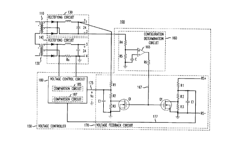
Referring initially to FIGURE 1, illustrated is one embodiment of a DC power
supply 100 constructed according to the principles of the present invention.
The DC
power supply 100 includes a first and second isolation transformer 110, 120
(each
having a primary and a secondary winding) coupled to a first and second output
rectifying circuit 130, 140, respectively. In the illustrated embodiment, the
first and
second transformers 110, 120 have the same turns ratio. The first and second
transformers 110, 120 are series-coupled, thereby evenly dividing an output
current of
the DC power supply 100 between the first and second output rectifying
circuits 130,
140. Those skilled in the art should understand, however, that a single
transformer
may also be used. The DC power supply 100 further includes an adaptive voltage
controller 150 for controlling an output of the DC power supply 100.
In one embodiment of the present invention, the first and second output
rectifying circuits 130, 140 each include a rectifier diode and a filter
capacitor. In a
preferred embodiment, the first and second output rectifying circuits 130, 140
each
include a pair of rectifier diodes, an output inductor, and a filter
capacitor. The first
and second output rectifying circuits 130, 140 are couplable in alternative
parallel and
series configurations to provide dual voltages at the output of the DC power
supply
2 0 100. In the illustrated embodiment, the dual voltages are +24 VDC and -48
VDC. Of
course, the DC power supply 100 may be configured to supply other voltages and
more
than two voltages. The first and second output rectifying circuits 130, 140
are
couplable as follows. In the parallel configuration, a first and second
terminal 1, 2 are
coupled to a third and fourth terminal 3, 4 respectively. In the series
configuration, the
2 5 second and third terminals 2, 3 are coupled together and the output
voltage is provided
across the first and fourth terminals 1, 4.
The voltage controller 150 includes a configuration determination circuit 160,
coupled to the output of the DC power supply 100, that generates a
configuration
signal 167 that is a function of a configuration of the first and second
output rectifying
CA 02241585 1998-06-23
-6-
circuits 130, 140. In this embodiment of the present invention, the
configuration
determination circuit 160 consists of a comparator 165 and its associated
components
(i.e., resistors R4, R5, reference voltage source Vref). The voltage
controller 150
further includes a voltage feedback circuit 170, coupled to the configuration
determination circuit 160, that develops output voltage feedback signals 175,
177
based on the configuration signal 167. The voltage feedback circuit 170
consists, in
this embodiment, of two circuits, each having a resistor ladder formed from a
first,
second, and third resistor R 1, R2, R3, coupled to a resistor bypass switch Q
1. Those
skilled in the art should realize that the voltage feedback circuit 170 may,
in alternative
embodiments, consist of one or more circuits, developing one or more voltage
feedback signals. The voltage feedback signals 175, 177 of the two circuits
represent,
respectively, the output voltage sensed at the output of the DC power supply
100 and
at a load (not shown). The voltage feedback signals 175, 177 may operate
alternatively
as required by the DC power supply 100. The voltage controller 150 still
further
includes a voltage control circuit 180, coupled to the voltage feedback
circuit 170. The
voltage control circuit 180 consists of, in this embodiment, a set of
comparison circuits
185, 187 that receives the voltage feedback signals 175, 177. Of course, the
use of any
number of comparison circuits is within the broad scope of the present
invention. The
voltage control circuit 180 uses the voltage feedback signals 175, 177 to
control the
2 0 output voltage of the DC power supply 100 as a function thereof. Those
skilled in the
art are familiar with closed loop feedback circuits, and, as a result, an
operation of the
voltage control circuit 180 will not be described in detail. Additionally, the
voltage
control circuit 180 may use the voltage feedback signals 175, 177 to initiate
under-
voltage and over-voltage shutdown.
2 5 The present invention therefore introduces the broad concept of adapting
the
voltage feedback signals 175, 177 in the voltage controller 150 to accommodate
different output voltages. This allows the single voltage controller 150 to
control a
dual-voltage DC power supply at either of its output voltages. While the power
supply
100 is a dual-voltage power supply, the scope of the present invention is not
so limited.
3 0 The operation of conventional DC power supplies should already be familiar
to
CA 02241585 1998-06-23
_'J_
those skilled in the art, and, as a result, the operation thereof will not be
described in
detail. The voltage controller 150 operates as follows. The configuration
determination circuit 160 senses the output voltage of an output terminal of
one of the
output rectifying circuits 130, 140. In the illustrated embodiment, the
configuration
determination circuit 160 senses the output voltage of the second terminal 2.
The
output voltage of the second terminal 2 is either +24 VDC or ground,
indicating the
configuration of the first and second output rectifying circuits 130, 140. If,
for
instance, the first and second output rectifying circuits 130, 140 are
configured in series
to provide -48 VDC, the second and third terminals 2,3 will be coupled
together. The
output voltage of the second terminal 2 will, therefore, be +24 VDC. If,
however, the
first and second output rectifying circuits 130, 140 are configure in parallel
to provide
+24 VDC, the output voltage of the second terminal 2 will be ground (0 VDC).
The
comparator 165 of the configuration determination circuit 160 thus generates
the
configuration signal 167 from the output voltage of the second terminal 2.
In the illustrated embodiment of the present invention, the configuration
signal
167 assumes a discrete value (e.g., a logic zero or logic one) as a function
of the
configuration. Alternatively, the configuration signal 167 may be continuously
variable
or of another function. The present invention is not limited to a particular
form of
configuration signal 167.
2 0 The configuration signal 167 is used by the voltage feedback circuit 170
to
generate the voltage feedback signals 175, 177. In the illustrated embodiment,
the
resistance of the resistor ladder is a function of the configuration signal
167. The
configuration signal i67 either enables or disables a resistor bypass switch
Q1, altering
the overall resistance of the resistor ladder, and thereby producing the
voltage feedback
2 5 signals 175, 177.
The comparison circuits 185, 187 of the voltage control circuit 180 then
compare the voltage feedback signals 175, 177 to reference voltages to control
the
output voltage: Additionally, the comparison circuits 185, 187 may initiate
under-
voltage and over-voltage shutdown of the power supply 100. Those skilled in
the art
3 0 are familiar with conventional control techniques based on feedback and
development
CA 02241585 1998-06-23
_g_
of error signals.
Turning now to FIGURE 2, illustrated is another embodiment of a DC power
supply 200 constructed according to the principles of the present invention.
The DC
power supply 200 includes a first and second isolation transformer 210, 220
coupled to
a first and second output rectifying circuit 230, 240, respectively. In the
illustrated
embodiment, a first output of the first rectifying circuit 230 is provided
across first and
second terminals 1, 2. A second output of the second rectifying circuit 240 is
provided
across third and fourth terminals 3, 4. The DC power supply 200 further
includes an
adaptive voltage controller 250 for controlling an output of the DC power
supply 200.
The first and second output rectifying circuits 230, 240, each include a first
and
second rectifier diode, an output inductor, and a filter capacitor.
Alternatively, the first
and second output rectifying circuits 230, 240 may each include a rectifier
diode and a
filter capacitor. Those skilled in the art should realize that the output
inductor and
second rectifier diode are not an integral part of the first and second output
rectifying
circuits 230, 240. The first output rectifying circuit 230 further includes a
first output
diode 235. The second output rectifying circuit 240 further includes a second
output
diode 245. The first and second output rectifying circuits 230, 240 are, of
course,
couplable in alternative parallel and series configurations.
The voltage controller 250 includes a configuration determination circuit 260,
2 0 coupled to the output of the DC power supply 200, that generates a
configuration
signal 267 that is a function of a configuration of the first and second
output rectifying
circuits 230, 240. The voltage controller 250 further includes a voltage
feedback
circuit 270, coupled to the configuration determination circuit 260, that
develops
voltage feedback signals 275, 277 based on the configuration signal.
2 5 The voltage controller 250 further includes a voltage control circuit 280,
coupled to the voltage feedback circuit 270. The voltage control circuit 280
consists
of, in this embodiment, a set of comparison circuits 285, 287 that receives
the voltage
feedback signals 275, 277 and controls the output voltage of the DC power
supply 200
as a function thereof. In the illustrated embodiment, the voltage control
circuit 280 is a
3 0 conventional closed loop feedback circuit; familiar to those skilled in
the art. The
CA 02241585 1998-06-23
-9-
comparison circuits 285, 287 compare the voltage feedback signals 275, 277 to
a
reference voltage and produce therefrom pulse width modulated drive signals to
control
switches in a power stage of the DC power supply 200.
The voltage controller 250 still further includes a diode bypass circuit 290,
coupled to the second output diode 245, that receives the configuration signal
from the
configuration determination circuit 260 and bypasses the output diode as a
function
thereof. In the illustrated embodiment, the diode bypass circuit 290 consists
of a relay.
Of course, any type of bypass circuit may be used.
The operation of the DC power supply 200 is substantially similar to the
operation of the DC power supply 100 of FIGURE 1 and will not be described in
detail. In the illustrated embodiment, the second and third terminals 2, 3,
are coupled
together, configuring the first and second output rectifying circuits 230, 240
in series to
provide -48 VDC. The configuration determination circuit 260, coupled to the
second
terminal 2, thus senses +24 VDC. Alternatively, the first and second output
rectifying
circuits 230, 240 may be configured in parallel to provide +24 VDC. The
configuration
determination circuit 260 would then sense 0 VDC (ground).
The first and second output diodes 235, 245 protect the first and second
output
rectifying circuits 230, 240, respectively, when the first and second output
rectifying
circuits 230, 240 are coupled in a parallel configuration. The second output
diode 245
2 0 is not required, however, when the first and second output,rectifying
circuits 230, 240
are series-configured. The diode bypass circuit 290, therefore, bypasses the
second
output diode 245 as a function of the configuration signal. By bypassing the
second
output diode 245, any inefficiency associated therewith is eliminated. Of
course, the
number of diode bypass circuits may vary depending on the number of output
rectifying
2 5 circuits.
In the illustrated embodiment, the first and second output rectifying circuits
230, 240 are in series. The +24 VDC sensed by the configuration determination
circuit
260 may thus be used to drive the diode bypass circuit 290 to bypass the
second output
diode 245. Alternatively, if the first and second output rectifying circuits
230, 240 are
3 0 in parallel, the 0 VDC (ground) sensed by the configuration determination
circuit 260
CA 02241585 1998-06-23
-10-
may be used to turn off the diode bypass circuit 290, thereby leaving the
second output
diode 245 in the circuit.
Although the present invention has been described in detail, those skilled in
the
art should understand that they can make various changes, substitutions and
alterations
herein without departing from the spirit and scope of the invention in its
broadest form.