Note: Descriptions are shown in the official language in which they were submitted.
CA 02241819 1998-06-29
MOTION ACTIVATED ILLUMID111TINO FOOT~1I~71erR AldD
LIC~RT MODULE THEREfOA WITH
CONTINUOUS/SEQUENTIAL 08CILLATINO LIDI~T6
~~,CK ROUND OF ;~'HE NVENTION
This invention relates to footwear, and more
particularly, is directed to motion activated
illuminating footwear having a light module therein.
It is well known to position a light inside of a
heel of footwear, with the light being activated all of
the time. In such known construction, the light can be
turned off by means of a switch extending from the heel
of the footwear. See, for example, U.S. Patent No.
4,253,253 to McCormick. However, this construction
provides certain disadvantages. First, there is the
possibility that the switch is not turned off, in which
case the light will burn out in a very short period of
time. Second, a connection must be made between the
switch on the outside of the heel to the circuitry within
the heel, which adds to the cost and complexity of the
footwear. Third, there is the possibility that the
switch can be damaged, for example, by banging the shoe
against an object, since the switch is externally
accessible.
For the above reasons, it is preferred to position
the entire circuitry and switch therefor entirely within
the heel of the footwear. In this regard, it is well
known to position a light, such as a light emitting diode
(LED) inside of the heel of footwear, such that the light
is visible from the exterior of the footwear, with the
light being activated by means of a pressure sensitive
switch. In particular, when the wearer steps down and
exerts pressure on the pressure sensitive switch when
walking or running, a circuit is closed so as to supply
power to activate the LED. When the wearer steps up.
relieving pressure from the pressure sensitive switch,
the circuit is opened so as disconnect power to the LED.
Examples of such footwear are disclosed in U.S. latent
Nos. 5,188,447 to Chia~g et al, European Patent
CA 02241819 2001-11-13
2
Application No. 0 12:1 026, and U.;~. Patent No. 3,800,133 to
Duval. However, the use of a pressure sensitive switch and
the associated circuit. connections increases the cost and
complexity of the foot=wear.
It is also known to position a light inside of the heel
of footwear, with the light being activated by a mercury tilt
switch in the footwear. See, for example, German
Offenlegungsschrift No. 2,608,485, the aforementioned European
Patent Application No.. 0 121 026, U.S. Patent No. 4,158,922 to
Dana, III, U.S. Patent. No. 4,848,009 to Rodgers and U.S.
Patent No. 3,893,247 too Dana, III. However, the addition of
the mercury tilt switc=h and the associated circuitry greatly
adds to the cost and complexity of the footwear.
U.S. Patent No. 5,408,764 to wut, discloses the use of an
LED inside of the heel of a shoe, which is intermittently
activated by movement of the shoe. Specifically, when the
shoe is moved, the free end of a coil spring which is fixed in
a cantilevered manner, is caused to intermittently complete
the electrical circuits to supply current to the LED.
It is further known to provide oscillating or sequential
illumination of LEDs, For example, in U.S. Patent No.
5,438,488 to Dion, six LEDs are distributed along a plastic
strip of the sneaker ~~etween the crossed laces, each of which
is turned on in sequence so as to give the appearance of a
light traveling along the strip as the LEDs are successively
turned on. In order t=o accomplish this purpose, a decade
counter has six outputs, each being connected to a respective
LED to provide such sequential lighting. However, since the
LEDs are controlled tc-_a operate sequentially and thereby
produce a sequential "'flashing" effect, there is no need to
provide a pressure sensitive switch, mercury tilt switch or
coil switch, as indicated above, to provide alternating power
to the circuit. In other words, in the
CA 02241819 1998-06-29
3
aforementioned circuits, the switches are activated to
turn on and off in response to movement of the shoe in
order to produce the flashing effect, while Dion produces
the flashing effect by reason of the decade counter so
that there would be no reason to provide any of the
aforementioned movement sensitive switches for powering
the decade counter in Dion. See also U.S. Patent No.
5,599,088 which discusses an alternative to a motion
sensitive switch, that is, flashing LEDs based on a
predetermined pattern.
Other circuits which provide alternating or
sequential flashing of LEDs are known in conjunction with
capacitors which charge and discharge to activate the
respective LEDs. Sae, for example, U.B. Patent No.
2,916,670 to Pederson for a-static flasher system; U.s.
patent No. 5,013,972 to Malkieli et al for another static
flasher system for use with a symbolic/religious memorial
light; U.S. Patent No. 2,960,627 to Hunt; and U.s. Patent
No. 3,631,359 to Jones. However, none of these patents
discloses use of such a circuit with a shoe or with a
motion sensitive switch for powering the oscillation
circuit.
OB;.TE~TS AND ~SUMMP.RY OF THE INVENT ON
Accordingly, it is an object of the present
invention to provide motion activated illuminating
footwear that overcomes the problems With the
aforementioned prior art.
It is another object of the present invention to
provide motion activated illuminating footwear in which a
plurality of lights are caused to sequentially or
alternately illuminate.
It is still another object of the present invention
to provide motion activated illuminating footwear in
which an oscillation circuit provides alternate
illumination of LEDs and is powered by a motion sensitive
switch in the footwear.
CA 02241819 1998-06-29
4
It is still another object of the present invention
to provide motion activated illuminating footwear in
which the oscillation circuit includes oapacitive
elements which charge and discharge to provide the
alternating illumination effect.
It is a further object of the present invention in
which the motion sensitive switch that powers the
oscillation circuit is a cantilevered coil switch.
It is a still further object of the present
Zo invention to provide motion activated illuminating
footwear in which the LEDs are continuously illuminated
when the switch is closed, due to a bypass diode circuit,
and in which an oscillation circuit provides alternate
illumination of the LEDr for a short period of time when
the switch is opened.
In accordance with an aspect of the present
invention, alight module for use with a plurality of
light sources mounted tc footwear, includes a power
supply for supplying p~wwer, and an oscillation circuit
for supplying power to the light sources to sequentially
cause illumination of the light sources. A switch has an
open condition and a closed condition, and a power supply
transmission circuit is connected between the power
supply, the switch and the oscillation circuit for
supplying power from the power supply to the oscillation
circuit when the switch is closed and for ending the
supply of power from the power supply to the oscillation
circuit when the switch is open. A bypass circuit is
connected between the oscillation circuit and the switch
to disable the oacilla.tion circuit and continuously
illuminate the light sources when the switch is closed,
the bypass circuit being disabled when the switch is
open. A first capacitive device is connected with the
power supply transmission circuit for staring a charge
when the switch is closed and for discharging through the
power supply transmiession circuit when the awitah is
opened to cause the oscillation circuit to sequentially
CA 02241819 1998-06-29
supply power to the light sourcea and sequentially cause
illumination of the light sources until the stored charge
of the first capacitive device falls below a
predetermined value.
5 The oscillation circuit includes first and second
transistors, each having an input connected to the power
supply transmission circuit, and an output path, a first
series connection of the output path of the first
transistor with a first one of Che light sources, a
second series connection of the output path of the second
transistor with a second one of the light eourcea, with
the series connections being connected in parallel with
each other and between the power supply and the power
supply transmission circuit, and second and third
capacitive devices, the second capacitive device being
connected between the input of the first transistor and
the output path of the second transistor, and the second
capacitive circuit being connected between the input of
the second transistor and the output path of the first
transistor.
The bypass circuit includes a diode connected
between a junction of the output path of one of the first
and second transistors with the respective one of the
first and second light sources, and the switch.
Specifically, the bypass circuit includes a first diode
connected between a junction of the output path of the
first transistor with the first light source, and the
switch; and a second diode connected between a junction
of the output path of the second transistor with the
3o second light source, and the switch.
Each of the first, second and third capacitive
devices includes a capacitor. A first resistive circuit
is connected between the input of the first transistor
and the power supply transmission circuit; and a second
resistive circuit is connected between tha input of the
second transistor and the power supply transmission
circuit.
CA 02241819 1998-06-29
6
The power supply transmission circuit includes a
transistor having an input connected with the switch, and
an output path connected between the power supply and the
oscillation circuit. The first capacitive device is
connected between one terminal of the power supply and
the input of the transistor.
The switch includes a motion activated switch
connected between an opposite terminal of the power
supply and the input of the transistor and which
alternately opens and closes a connection between the
power supply and the input of the transistor during
movement of the light module and which opens the
connection between the power supply and the input of the
transistor when the light module stops moving.
Specifically, the motion activated switch includes a
spring switch connected in a cantilevered manner such
that one end of the spring switch is electrically
connected to one of the power supply and the power supply
transmission circuit, and an opposite free end of the
spring switch intermittently electrically connects with
the other of the power supply and the power supply
transmission circuit during movement of the light module.
Each light source includes a light emitting diode.
In accordance with another aspect of the present
invention, a light module for use with a plurality of
light sources mounted to footwear, includes a power
supply for supplying power; an oscillation circuit for
sequentially supplying power to the light sources to
Sequentially cause illumination of the light sources; and
a switch circuit which supplies power to the oseiiiation
circuit during movement~of the light module and which
prevents the supply of power to the oscillation circuit
when the light module stops moving.
The above and other objects, features and advantages
of the invention will become readily apparent from the
following detailed description thereof which is to be
read in connection with the accompanying drawings.
CA 02241819 1998-06-29
7
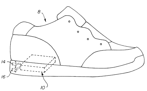
B~ DESCRIPTxON OF THE DRAWING&
Fig. 1 is a perspecaive view of a running shoe, with
the location of the light module shown in phantom
therein;
Fig. 2 is a bottom plan view of the running shoe of
Fig. 1, with the light module shown in phantom therein;
Fig. 3 is a partial7.y exploded perspective view of a
light module of the mot.'Lon activated illuminating
footwear according to one embodiment of the present
l0 invention;
Fig. 4 is a fully exploded perspective view of the
light module of Fig. 3;
Fig. 5 is a circuit wiring diagram showing the
equivalent electrical circuitry for the light module of
Fig. 3;
Fig. 6 is a circuit wiring diagram showing
electrical circuitry of a light module according to
another embodiment of the present invention;
Fig. 7 is a circu;~t wiring diagram showing a
modification of the circuit of Fig. 5 according to
another embodiment of the present invention; and
Fig. 8 is a circuit wiring diagram showing a
modification of the circuit of Fig. 5 according to still
another embodiment of the present invention.
n~'~~A_ZLE DE CRIPTIO OF THE PRE ERR D MBODIMENTS
Referring to the drawings in detail, and initially
to Figs. 1-5 thereof, footwear 8 such as a running shoe
or the like includes a Light module 10, according to a
first embodiment of tl~e present invention, incorporated
into the heel of the Footwear, in a similar manner to
U.S, Patent No. 5,408,764.
Light module l0 includes a printed circuit board 12
having various electrical components mounted thereon.
specifically, and referring to Figs. 3-5, light module 10
includes first and second LEDs 14 and 16 which are
sequentially or alternately illuminated by an oscillation
CA 02241819 1998-06-29
8
circuit l8 that is powered by a power supply 20 through a
motion sensitive switch circuit 22, as shown best in Fig.
5.
Specifically, power supply 20 can be comprised of a
three volt battery 24 which is mounted on printed circuit
board 12.
Motion sensitive switch circuit 22 is formed by a
coil spring 26 having one end 28 thereof fixedly mounted
to a spring holder 30 which, in turn, is mounted to one
end of an elongated printed circuit board 32. The
opposite end 34 of coil spring 26 is free, such that coil
spring 26 is mounted in a cantilevered manner on printed
circuit board 32. The opposite free end 34 of coil
spring 26 is mounted in spaced relation above a metal
arch 36 that is fixed to the opposite end of printed
circuit board 32. A weighting ball 3s is secured to the
free end 34 of coil spring 26. In the stationary
position of footwear 8, free end 34 is positioned
slightly above, but in spaced relation to, metal arch 36.
Spring holder 30, and thereby the fixed end 28 of coil
spring 26, are connected by an electric wire to printed
circuit board 12, while metal arch 36, and thereby free
end 34 of coil spring 26 when it contacts metal arch 36,
are also connected by an electric wire to printed circuit
board 12.
Coil spring 26 and printed circuit board 32 are
enclosed by an arcuate spring housing 40 having an end
closure cap 42. Printed circuit board 32 can be secured
to spring housing 40 or end closure 42 to provide a
unitary assembly.
As shown in Fig. 5, motion sensitive switch also
includes a transistor 44 having its emitter-collector
path connected between the positive terminal of power
supply 20 and oscillation circuit 18, and its base
connected to the negative terminal of power supply 30
through a series circuit of a resistor 46 and coil spring
26. Further, a capacitor 48 is connected in parallel
CA 02241819 1998-06-29
9
with the series circuit of resistor 46 and the emitter-
base path of transistor 44. In other words, one terminal
of capacitor 48 is connected to the function between
resistor 46 and coil apring 26, and the other terminal of
capacitor 48 is connected to the function between the
emitter of transistor 44 and the positive terminal of
power supply 20.
With this arrangement, when free end 34 of coil
spring 26 contacts metal arch 36 so as to close switch
circuit 22, capacitor 48 will be charged and will build
up a voltage at the base terminal of transistor 44. As a
result, transistor 44 will turn on, causing current to
flow through the emitter-collector path of transistor 44,
which will be supplied to oscillation circuit 18. When
free end 34 of coil spring 26 is out of contact with
metal arch 36, the charge on capacitor 48 will maintain
transistor 44 in an on condition so that current will
still flow through the emitter-collector path thereof to
oscillation circuit 18. Therefore, alternate contact of
free end 34 with arch 36 will result in transistor 44
being maintained in an on condition.
When the shoe is stationary for a period of time,
capacitor 48 will discharge through the base of
transistor 44, thereby maintaining transistor 44 in an on
condition until the charge on capacitor 48 falls below
the threshold value necessary to turn transistor on, at
which time transistor 44 will turn off, thereby closing
the emitter-collector path thereof and preventing the
supply of current to oscillation circuit 18.
Oscillation circuit 18 includes two transistors 50
and 52 having their emitters connected together and also
connected to the negative terminal of power supply 20.
The base of transistor 50 is connected to the
collector-emitter path of transistor 44 through a
resistor 54, while the base of transistor 52 is connected
to the collector-emitter path of transistor 44 through a
resistor 5G. The collector of transistor 50 is connected
CA 02241819 1998-06-29
to the cathode of LED 14, with the anode thereof
connected to the collector°emitter path of transistor 44,
while the collector of transistor 52 is connected to the
cathode of diode l6, with the anode thereof connected to
5 the collector-emitter path of transistor 44.
Finally, a capacitor 58 is connected between the
base of transistor 50 and the collector of transistor 52,
while a capacitor 60 is connected between the base of
transistor 52 and the collector of transistor 50.
10 Capacitors 58 and 60 have different charging times.
With power being supplied to oscillation circuit 18,
transistors 50 and 52 will both try to turn on. This
will cause current to start to flow through LED 14 and
the collector-emitter path of transistor 50 so as to
start to illuminate LED 14 and, at the same time, since
transistor 52 is also trying to turn on, current will
flow through LED 16 and the collector-emitter path of
transistor 52 to start to illuminate LED 16. The effect
of this is to reduce the collector-emitter voltage of
both transistors.
If it is assumed that transistor 52 reaches
saturation first, its collector-emitter voltage is so low
and the capacitor 58 has had so little time to charge,
that the resulting voltage on the base of transistor 50
becomes too low to keep it on. As a result, transistor
50 turns off arid most of the charge on capacitor 60 is
dissipated because the voltage on both sides of that
capacitor will be at the supply voltage level. With
transistor 50 off and transistor 52 on, capacitor 58
charges and the voltage on the base of transistor 50
increases .until it turns on. when transistor 50 on, its
collector-emitter voltage drops very low, which in turn
causes the voltage on the base of transistor 52 to drop,
cutting the transistor off. With transistor 52 off,
capacitor 60 begins to charge until transistor 52 turns
on again, which has the effect of turning transistor 50
off. This alternating turning on and off of transistors
CA 02241819 1998-06-29
11
50, 52 repeats at a rate determined by the time constant
of resistor 56 and capacitor 60 for one half of the cycle
and resistor 54 and capacitor 58 for the other half
cycle.
As a result, LEDs 14 and 16 are alternately or
seguentially illuminated, as long as power is supplied to
the circuit, that is, as long as motion sensitive switch
22 supplies power to oscillation circuit 18.
When the free end of coil spring 26 is out of
contact with arch 36 for a long enough period of time,
that is, when the shoe is stationary, the charge on
capacitor 48 is reduced to a level to turn off transistor
44 so that there is no power supplied to oscillation
circuit 18. At this time, oscillation circuit 18 will
stop operating.
While the shoe is in motion, the switch may bounce,
making periodic contact. As long as this contact is more
frequent than the discharge rate of capacitor 48, the
transistor 44 will remain on, supplying power to the
oscillator circuit, so that LEDs l4 and 16 will continue
to oscillate, that is, flash on and off alternately.
Thus, the only time that LEDs 14 and 1G stop the
alternating illumination is when there is a transition of
switch circuit 22 from an on state to an off state, and
capacitor 48 has discharged enough to causB transistor 44
to turn off.
Referring to Fig. 6, there is shown a modification
of the circuit of Fig. 5 in that two LEDs 14a and 14b arc
provided in parallel, in place of the single LED 14 of
Fig. 5. With this circuit, LEDs 14a and 14b are
illuminated together and alternate with LED 16. Tn other
words, LED 16 is first illuminated, followed by both LEDs
14a and 14b, then followed by LED 16, and so on.
Referring to Fig. 7, there is shown a modification
of the circuit of Fig. 5 in that a diode 70 is connected
between the junction of resistor 46 and switch 2G and the
junction of the collector of transistor 52 and LED 16.
CA 02241819 1998-06-29
12
In addition, a diode 72 is connected between the junction
of resistor 46 and switch 26 and the junction of the
collector of transistor 50 and LED 14. Diodes 70 and 72
constitute bypass circuits.
By use of the extra diodes 70 and 72 in Fig. 7,
which are connected between the collectors of the
transistors 52 and 50 of the oscillation circuit at one
end, and the junction of coil spring switch 26 with
capacitor 48 at the other end, when coil spring switch 26
is closed, there will be a constant illumination of LEDs
14 and 16, that is, oscillation circuit is will not
function to provide oscillation, but will continuously
illuminate LEDs l4 and 16. This is because there will bs
a path from the positive terminal of battery 24 through
transistor 44, LEDs 14, 16; diodes 70, 72; and switch 26
to the negative side of the battery 20. The effect is to
continuously illuminate LEDs 14 and 16.
When coil spring switch 26 is opened, diodes 14 and
l6 function to block current flowing therethrough, that
is, since switch 26 is opened, the circuit through diodes
14 and 16 is open. However, power is supplied to the
oscillating circuit because the stored charge in
capacitor 48 holds transistor 44 on. Accordingly, since
there is no bypass through diodes 70 and 72, oscillation
circuit is functions as an oscillation circuit in order
to provide oscillation of LEDs 14 and 16 therein, during
discharge of capacitor 4~. Thus, current flow is through
LEDs 14 and 16 and the r.:ollactvr-emitter paths of
transistors 50 and 52 of oscillation circuit 18. When
the charge on capacitor 48 reduces to a certain level,
power transistor 44 wild turn off and cut off power to
oscillation circuit 18.
Thus, the circuit o~ Fig. 7 operates to continuously
illuminate LEDs l4 and 16 as long as switch 26 is closed
and to illuminate LEDs in a predetermined sequence upon
opening of switch 26. As the charge on capacitor 48
discharges, the voltage at the collector of transistor 44
CA 02241819 1998-06-29
13
reduces. If capacitor ~l8 is rQlatively large, so that it
takes at least a couple Qf seconds to discharge, while
the LEDs alternately flash due to the operation of the
oscillator circuit 18, the intensity of the flashes Will
decrease. The result is a fading alternating flashing
effect.
The same result shown in Fig. 7 can also be achieved
by the circuit in Fig. 8 in which only one diode 70 is
provided, that is, with diode 72 eliminated, although it
is preferred to have both diodes ?0 and 72.
Alternatively, diode 72 can be provided and diode 70
eliminated.
Having described specific preferred embodiments of
the invention with reference to the aocompanying
drawings, it will be appreciated that the present
invention is not limited to those precise embodiments and
that various changes and modifications can be effected
therein by one of ordinary skill in the art without
departing from the scope or spirit of the invention as
defined by the appended claims.