Note: Descriptions are shown in the official language in which they were submitted.
CA 02242195 1998-07-03
DESCRIPTION
METHOD AND DEVICE FOR RECORDING DATA IN OPTICAL MEMORY CARD
TECHNICAL FIELD
The invention relates to a method and a device for
recording data in an optical memory card, and more
particularly to a method and a device for recording data in an
optical memory card, that records data so as to form at least
one record pit between two data records in a recording region
of the optical memory card in order to improve a function of
fudging between an unrecorded region and a recorded region of
the optical memory card, thereby preventing double writing.
BACKGROUND ART
Generally, the optical memory card is a plastic card and
can record and reproduce data in its recording region with a
laser beam.
Fig. 7 shows a recording region 102 of an optical memory
card 101. As shown in its enlarged diagram, data recording
tracks 103 for recording information and guide tracks 104
formed at given intervals required for tracking control for
stabilizing a radiating position of the laser beams for
recording and reproducing are alternately disposed on the
recording region 102.
The data recording tracks 103 and the guide tracks 104
have a different reflection ratio. Comparing the reflection
ratio of these two, the data recording tracks 103 have a
higher reflection ratio and the guide tracks 104 have a lower
1
CA 02242195 1998-07-03
reflection ratio.
And, a record pit 105 is a portion having a low
reflection ratio, which is formed in the data recording tracks
103, with the laser beam to record information. The presence
or not of the record pit 105 indicates information to be
recorded.
Fig. 8 shows a logical data structure of the recording
region 102. On the recording region 102, read-in 111 provided
for an unillustrated optical memory card reader/writer to
realize a bit synchronization at the time of recording or
reproducing and an SYNC mark 112 for the unillustrated optical
memory card reader/writer to realize a frame synchronization
at the time of recording or reproducing have been recorded, in
addition to a data recording region 110 where information is
recorded.
The read-in 111 has the SYNC mark 112 recorded and record
pits 105 formed at given intervals.
An optical memory card reader/writer (not shown) is
provided with a synchronization signal generator (not shown),
scans the optical memory card 101 at a scan rate so that a
synchronization signal output from the synchronization signal
generator agrees with a signal which rises for every one bit
detected by scanning the read-in 111, and keeps the same scan
rate to make bit synchronization.
And, the SYNC mark 112 is formed of record pits 105,
which are arranged in a pattern not produced by modulation,
and used when the unillustrated optical memory card
reader/writer gets frame synchronization.
2
CA 02242195 1998-07-03
The frame is a bit separation to process a signal by a
signal processing circuit in the unillustrated optical memory
card reader/writer. The unillustrated optical memory card
reader/writer is provided with a counter (not shown) for
obtaining frame synchronization. The counter counts the
synchronization signal, outputs a frame synchronization signal
after counting up to the number of bits configuring one frame,
and resets its counted number.
Since the SYNC mark 112 is recorded at the start end (or
termination end) of the frame, the unillustrated optical
memory card reader/writer scans the optical memory card 101.
And when the SYNC mark 112 is detected, the number indicated
by the unillustrated counter for obtaining frame
synchronization is reset, thereby assuring the acquisition of
frame synchronization.
And, the data recording region 110 has the SYNC mark and
n sectors 113 arranged as indicated by a data recording region
110-1 on each frame. The sector 113 is composed of a single
or a plurality of bits.
Fig. 9 is a diagram showing an NRZI-RZ (nonreturn-to-zero
change on 1-return to zero) modulation system for converting
data, which is recorded in a conventionally used optical
memory card, into the presence or not of a record pit.
The NRZI-RZ modulation system is a modulation system to
produce a pulse at a polarity reversion position of an NRZI
(nonreturn-to-zero change on 1) modulation system.
When data shown in Fig. 9 (a) is modulated, the NRZI
modulation system reverses the polarity of a signal at the bit
3
CA 02242195 1998-07-03
midpoint of data "1" as shown in Fig. 9 (b).
Accordingly, the NRZI-RZ modulation system generates a
pulse at a polarity reversion position of Fig. 9 (b) as shown
in Fig. 9 (c).
Data modulated by the NRZI-RZ modulation system is
recorded by forming a record pit in the recording region of
the optical memory card so as to correspond to the position of
the pulse as shown in Fig. 9 (d).
As apparent from Fig. 9 (a) and Fig. 9 (d), the NRZI-RZ
modulation system does not form a record pit on a part where
data "O" is continuous.
However, before recording data on the optical memory
card, the optical memory card reader/writer reproduces the
optical memory card to detect the presence or not of a record
pit. Thus, it judges between an unrecorded region and a
recorded region of the optical memory card to prevent double
writing on it. Therefore, if data to be recorded in the
optical memory card has a portion where data "O" is
continuous, a record pit is not formed on the optical memory
card while data "O" is continuing. And, it becomes hard to
judge between the unrecorded region and the recorded region,
resulting in degrading a function of preventing double writing
from being made by the optical memory card reader/writer.
SUNINIARY OF THE INVENTION
Under the circumstances described above, it is an object
of the invention to provide a method and a device for
recording data in an optical memory card, which records data
4
CA 02242195 1998-07-03
by a modulation system which forms a record pit even when data
to be recorded has data "0" which continues, and changes the
modulation system of a card recorded by the NRZI-RZ modulation
system, to facilitate judgment between an unrecorded region
and a recorded region of the optical memory card, thereby
keeping a function of preventing double writing from being
made by an optical memory card reader/writer.
In order to achieve the above object, the invention
relates to a method of recording data in an optical memory
card, in which data is recorded in such a manner as to form at
least one record pit between two data records in a recording
region of the optical memory card.
The recording region of the optical memory card comprises
one-bit sectors in one frame, the data is modulated by an
NRZI-RZ modulation system to record it in a sector for
recording data and to reproduce a sector adjacent to the
sector for recording data, and if the adjacent sector~has been
recorded and the record pit has not been formed in both the
sector for recording data and the adjacent sector, a record
pit is formed on a boundary between the sector for recording
data and the adjacent sector.
The recording region of the optical memory card comprises
plural-bit sectors in one frame, the data is modulated by an
MFM-RZ modulation system to record it in a sector for
recording data and to reproduce a sector adjacent to the
sector for recording data, and if the adjacent sector has been
recorded and the record pit has not been formed in both the
sector for recording data and a record position in contact
CA 02242195 1998-07-03
with a boundary of the adjacent sector, a record pit is formed
on a boundary between the data-recorded sector and the
adjacent sector.
The data is reproduced when the recording region of the
optical memory card has data recorded by the NRZI-RZ
modulation system, and the record pit is formed on a boundary
of the record positions so as to modify to record by the
MFM-RZ modulation system when the recording region of the
optical memory card has continuous record positions where the
record pit has not been recorded.
The invention also relates to a device for recording data
in an optical memory card, which comprises means for recording
data in such a manner as to form at least one record pit
between two data records in a recording region of the optical
memory card.
The recording region of the optical memory card comprises
one-bit sectors in one frame, and wherein the recording device
comprises means for modulating the data by an NRZI-RZ
modulation system to record it in a sector for recording data,
means for reproducing a sector adjacent to the sector for
recording data, and means for forming the record pit on a
boundary between the sector for recording data and the
adjacent sector if the adjacent sector has been recorded and
the record pit has not been formed in both the sector for
recording data and the adjacent sector.
And, the recording region of the optical memory card
comprises plural-bit sectors in one frame, and wherein the
recording device comprises means for modulating the data by an
6
CA 02242195 1998-07-03
MFM-RZ modulation system to record it in a sector for
recording data, means for reproducing a sector adjacent to the
sector for recording data, and means for forming the record
pit on a boundary between the sector for recording data and
the adjacent sector if the adjacent sector has been recorded
and the record pit has not been formed in both the sector for
recording data and a record position in contact with a
boundary of the adjacent sector.
Besides, the data recording device further comprises
means for reproducing the data when the recording region of
the optical memory card has data recorded by the NRZI-RZ
modulation system, and means for forming a record pit on a
boundary of the record positions so as to modify to record by
the MFM-RZ modulation system when the recording region of the
optical memory card has continuous record positions in which
the record pit has not been recorded.
BRIEF DESCRIPTION OF THE DRAWINGS
Figs. 1(a) to 1(c) are diagrams showing an embodiment to
record data on sectors of one bit in one frame;
Fig. 2 is a diagram showing the data structure of the
data recorded in the embodiment shown in Fig. 1 on a memory in
a card reader/writer;
Figs. 3(a) to 3(e) are diagrams showing an example of
data modulation by an MFM-RZ modulation system;
Figs. 4(a) to 4(c) are diagrams showing an embodiment to
record data on sectors of a plurality of bits in one frame;
Fig. 5 is a diagram showing the data structure of the
7
CA 02242195 1998-07-03
data recorded in the embodiment shown in Fig. 4 on the memory
in the card reader/writer;
Figs. 6(a) to 6(c) are diagrams showing one example of
modifying a card recorded by an NRZI-RZ modulation system into
recordation by the MFM-RZ modulation system;
Fig. 7 is a diagram showing a recording region of an
optical memory card;
Fig. 8 is a diagram showing a logical data structure in a
recording region; and
Figs. 9(a) to 9(d) are diagrams showing an example of
data modulation by the NRZI-RZ modulation system.
BEST MODE FOR CARRYING OUT THE INVENTION
A method and device for recording data in an optical
memory card according to the invention will be described with
reference to the accompanying drawings.
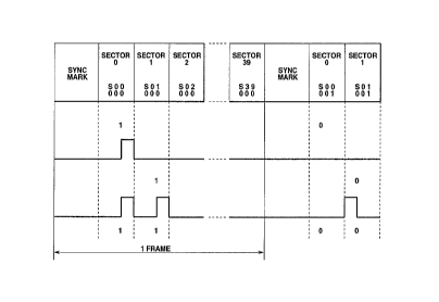
Fig. 1 shows an embodiment in that data is recorded in
one-bit sectors in one frame. Fig. 2 shows a data structure
on a memory in a card reader/writer (not shown) of data to be
recorded in the embodiment shown in Fig. 1.
Description will be made of an MFM-RZ (modified frequency
modulation-return to zero) modulation system with reference to
Fig. 3.
The MFM-RZ modulation system is a modulation system to
generate a pulse in a polarity reversion position of an MFM
(modified frequency modulation) system.
When data shown in Fig. 3 (a) is modulated, the MFM
system reverses a polarity at a bit midpoint of data "1" and a
8
CA 02242195 1998-07-03
bit division position where data "0" is continuous as shown in
Fig. 3 (b).
Accordingly, the MFM-RZ modulation system produces a
pulse at the polarity reversion position of Fig. 3 (b) as
shown in Fig. 3 (c).
And, a conventionally used NRZI-RZ (nonreturn-to-zero
change on 1-return to zero) modulation system is a modulation
system (see Fig. 3 (e)) which generates a pulse at a polarity
reversion position of an NRZI (nonreturn-to-zero change on 1)
modulation system (see Fig. 3 (d)).
When data "O" is continuous, the NRZI-RZ modulation
system does not generate a pulse, while the MFM-RZ modulation
system generates a pulse between at least two recording
intervals.
Therefore, when data with continuous repeated "O" is
reproduced, the NRZI-RZ modulation system cannot distinguish
the region having the continuous data "O" from an unrecorded
region, while the MFM-RZ modulation system can distinguish.
To record data in one-bit sectors in one frame as shown
in Fig. 1 (a), data is stored on the memory in a reader/writer
(not shown) as shown in Fig. 2, in which data of sector O is
arranged in direction X, and data of sector 0 to data of
sector 39 are arranged in order of increasing number in
direction Y.
When data of sector 0, e.g., data of 500000 = "1" and
S00001 = "0", are recorded in an unrecorded card, data are
recorded by the NRZI-RZ modulation system as shown in Fig. 1
(b). The NRZI-RZ modulation system is used because the sector
9
CA 02242195 1998-07-03
is composed of one bit in one frame, data is not recorded
continuously and data "0" is not continuous.
To record data of sector l, namely data of SO1000 = "1"
and 501001 = "O", into the card having its sector O already
recorded, data is also recorded by the NRZI-RZ modulation
system, and before or after recording the data, the data
recorded in sector 0 is reproduced, and a record pit is formed
on a boundary between sector 0 and sector 1 as shown in Fig. 1
(c) as required (when both data in sector 0 and sector 1 are
"0").
When data is recorded as described above, in the same way
as the MFM-RZ modulation system is used to record data, the
presence or not of a record pit can be detected to fudge
between the unrecorded region and the recorded region of the
optical memory card, and double writing in the optical memory
card can be prevented.
Fig. 4 shows an embodiment that data is recorded in
multiple-bit sectors in one frame. Fig. 5 shows the structure
of data, which is recorded in the embodiment shown in Fig. 4,
on the memory within a card reader/writer (not shown).
To record data in four-bit sectors in one frame shown in
Fig. 4 (a), data is stored in the memory within the
reader/writer (not shown) as shown in Fig. 5. In the card,
data 500000, S00272, 500544 and 500816 with X=0 shown in Fig.
are recorded in sector 0 of the first frame shown in Fig. 4
(a), and data S00001, S00273, S00545 and 500817 with X=1 as
shown in Fig. 5 are recorded in sector 0 of the second frame
as shown in Fig. 4 (a).
'v
CA 02242195 1998-07-03
To record data in four-bit sectors in one frame, the
MFM-RZ modulation system is employed. In view of the
structure of the sector, because data of at least four bits
are continuously recorded within one frame. Recording of data
of sector 0, e.g., data such as 500000 = "0", 500001 = "1",
500272 = "0", 500273 = "O", 500544 = "1", 500545 = "0", 500816
"O" and 500817 = "0" in an unrecorded card is as shown in
Fig. 4 (b).
Then, when data of sector 1 is recorded on the card
having sector 0 recorded, for example data of 510000 = "0",
510001 = "1" S10272 = "O" 510273 = "0" 510544 = "1" S10545
_ "O", 510816 = "O" and 510817 = "0" are recorded as shown in
Fig. 4 (c).
In this case, data of sector 0 is also reproduced before
or after recording data into sector 1 to form a record pit on
a boundary between sector O and sector 1 as required so to
have the same boundary between sector O and sector 1 as
recorded by the MFM-RZ modulation system.
Fig. 6 shows an example that a card recorded by the
NRZI-RZ modulation system is modified so to be recorded by the
MFM-RZ modulation system.
When the card recorded by the NRZI-RZ modulation system
is modified so to be recorded by the MFM-RZ modulation system,
the original card recorded by the NRZI-RZ modulation system
can be modified to adopt the MFM-RZ modulation system (same as
the MFM-RZ modulation system) by the same method even if data
are discontinuous as in the one-bit sectors in one frame or
data are continuous as in the sectors of a plurality of bits
11
Fe
CA 02242195 1998-07-03
in one frame.
Data "00000110100" as shown in Fig. 6 (a) becomes a
signal to generate a pulse at a bit midpoint of data "1" as
shown in Fig. 6 (b) by the NRZI-RZ modulation system, and a
record pit is formed on the card so to correspond to the
position where the pulse is generated.
Data shown in Fig. 6 (a) also becomes a signal to
generate a pulse at a bit midpoint of data "1" and at the
position of a bit breakpoint when data "0" is continuous by
the MFM-RZ modulation system as shown in Fig. 6 (c).
It is apparent from Fig. 6 (b) and Fig. 6 (c) that to
change the record made by the NRZI-RZ modulation system into
one made by the MFM-RZ modulation system, it is done
satisfactorily by additional formation of a record pit at the
position of a bit breakpoint when data "0" is continuous.
Therefore, the unillustrated card reader/writer
reproduces the card which was recorded by the NRZI-RZ
modulation system and forms a record pit on the card by the
MFM-RZ modulation system to record data, so that the NRZI-RZ
modulation system can be changed to the MFM-RZ modulation
system.
And, the unillustrated card reader/writer detects the
presence or not of a record pit in view of the reproduced
signal to fudge between the unrecorded region and the recorded
region of the optical memory card and extracts a
synchronization component from the reproduced signal as a data
signal. But, the record pit formed when the NRZI-RZ
modulation system is changed to the MFM-RZ modulation system
12
CA 02242195 1998-07-03
is not included in the synchronization component and does not
affect on the data signal. Therefore, the card modified to
the MFM-RZ modulation system can also be reproduced by a card
reader/writer of the NRZI-RZ modulation system.
INDUSTRIAL APPLICABILITY
The invention can be applied to a data recording method
and device for an optical memory card. The invention is
configured to record data to form at least one record pit
between two data records in a recording region of the optical
memory card and has an improved function for fudging between a
unrecorded region and a recorded region of the optical memory
card to facilitate prevention of double writing.
13