Note: Descriptions are shown in the official language in which they were submitted.
CA 02242287 2004-07-26
1
Connector
The invention relates to a high density connector,
comprising a housing of insulating material and a plurality of
signal and ground contacts regularly arranged in rows and
columns within said housing, each of said contacts having
first and second ends and an intermediate section, said first
ends each including a connection section, wherein said housing
is provided with a front wall having a grid of entrance
openings leading to said connection sections.
Document EP 0 446 980 A1 (Burndy Electra N.V.) published
on September 18, 1991, discloses a connector of this type. In
this known connector the signal contacts are mounted in a
dielectric insert surrounded by an outer conductor. Although
the impedance of the signal contacts can be determined in this
manner, manufacturing the connector is relatively complicated.
Further, increasing the density of the contacts would
significantly increase the complexity of the connector.
The invention aims to provide a connector of the above-
mentioned type wherein the impedance of the contacts can be
improved in a simple manner.
More specifically, according to the invention, there is
provided a receptacle connector with a high density of
contacts, comprising a housing of insulating material and a
plurality of signal and ground contacts regularly arranged in
rows and columns within the housing. Each of the contacts has
first and second ends and an intermediate section, the first
ends each including a receptacle contact connection section.
Also, the housing is provided with a front wall having a grid
of entrance openings leading to the connection sections. The
receptacle connector is characterized in that the housing is
provided with a common air chamber disposed adjacent the front
wall, a plurality of the receptacle contact connection
sections extending along a part of their length through this
common air chamber.
The foregoing and other objects, advantages and features
of the present invention will become more apparent upon
reading of the following non restrictive description of two
illustrative embodiments thereof, given by way of example only
with reference to the accompanying drawings in which:
CA 02242287 2004-07-26
1a
Fig. 1 shows a cross-section through a column of signal
contacts of a connector assembly comprising a male connector
and an illustrative embodiment of a female connector according
to the invention, wherein the connectors are disconnected.
Fig. 2 shows a cross-section through a column of ground
contacts of the female connector of Fig. 1.
CA 02242287 1998-07-06
2
Fig. 3 shows a front view of the female connector of
Fig. 1.
Fig. 4 shows a cross-section through a column of
signal contacts of a connector assembly comprising a second
embodiment of the female connector according to the inven-
tion.
Fig. 5 shows a front view of the female connector of
Fig. 4.
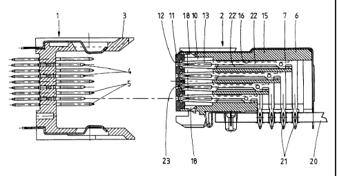
Referring to Figs. 1-3 there is shown a connector
assembly for printed circuit boards, comprising a male
connector 1 and a female connector 2. The male connector 1
comprises a first housing 3 of insulating material and a
plurality of male signal contacts 4 and a plurality of male
ground contacts 5. In the embodiment shown the length of the
ground contacts 5 is greater than the length of the signal
contacts 4. However, the signal and ground contacts may have
equal lengths.
The female connector 2 comprises a second housing 6
of insulating material and a plurality of female signal
contacts 7 and a plurality of female ground contacts 8,
wherein the ground contacts of one column are part of a
ground contact element 9 as shown in Fig. 2.
In order to increase the density of contacts, the
signal and ground contacts 4, 5 and 8, 9 are arranged in a
special manner as can be seen in the front view of the
female connector 2 in Fig. 3. All contacts are regularly
arranged in rows and columns, wherein in each row and column
all contacts 4, 5 and 8, 9 are arranged at an equal pitch p
in row and column direction. Further, each row and each
column of signal contacts 4 or 8 contains signal contacts
only and each row and each column of ground contacts 5 or 9
contains ground contacts only. As can be seen in Fig. 3,
successive rows of contacts 8, 9 are staggered in row
direction by half the pitch p of the contacts, wherein the
rows and columns of contacts have a pitch equal to half the
pitch p of the contacts. In this manner a pitch half p of
the contacts in adjacent rows and columns can be obtained.
CA 02242287 2004-07-26
3
At a pitch of for example 2 mm, the pitch between adjacent
contacts 4, 5 and 8, 9 will be 1 mm.
In the female connector 2, the impedance of the signal
contacts 7 is improved by providing the housing 6 with an air
chamber 10 at the front side of the connector 2. As shown in
Figs. 1 and 2, the housing 6 comprises a front wall 11 having
a grid of entrance openings 12 leading to fork-shaped
connection sections 13 of the signal and ground contacts 7, 8.
The housing 6 further comprises a contact supporting part 15
provided with passages 16 and 17 for the female signal
contacts 7 and ground contacts 8, respectively. As
schematically shown in Fig. 1, the front wall 11 is detachably
attached to the contact supporting part 15 by means of hooks
18.
As shown in FIG. 2, the female ground contacts 8 of one
column are part of a ground contact element 9 having a
plurality of press-fit terminations 19 connected to the plated
through-holes of a printed circuit board 20. The female signal
contacts 7 are also provided with press-fit terminations 21
connected to plated through-holes of the printed circuit board
20. The female signal contacts 7 having the connection section
13 as first end and the press-fit termination 21 as second
end, include an intermediate section 22 extending through the
corresponding passage 16 of the contact supporting part 15 of
the house 6.
As can be seen in Figs. 1 and 2 the connection sections
13 of the contacts 7, 8 extend through the air chamber 10 into
corresponding recesses 23 provided at the inner side of the
front wall 11 at the location of each entrance opening 12. In
this manner the recesses 23 receive and align the connection
sections 13 of the contacts with the corresponding entrance
openings 12.
CA 02242287 1998-07-06
4
The impedance of the signal contacts 7 is signifi-
cantly improved because the connection sections 13 extend
through air as dielectric. The impedance can be further
improved by a special design of the intermediate sections 22
of the signal contacts 7 as shown in Fig. 1. A part of the
intermediate section 22 is removed so that air is present as
dielectric along this removed length of the intermediate
sections as indicated by 22'. This means that the height of
the intermediate section 22 is less than the height of the
corresponding passage 16.
Fig. 4 shows a cross-section of a further connector
assembly comprising a male connector 24 and a female connec-
tor 25, wherein the female connector 25 is mainly in the
same manner as the female connector 2 of Figs. 1-3. However,
in this case the pitch of adjacent contacts is 2 mm and the
rows of contacts are not staggered as can be seen in the
front view of the female connector 25 shown in Fig. 5. The
housing 6 of the connector 25 is made in the same manner
with a front wall 11 and a contact supporting part 15,
wherein the connection sections 13 extend through an air
chamber 10 into recesses 23 at the inner side of the front
wall 11. Further the intermediate sections 22 of the female
signal contacts 7 are made in the same manner as in the
connector 7. In this manner again the impedance of the
signal contacts is improved.
Although the invention has been explained with
reference to a female connector for a printed circuit board,
it will be understood that the invention can also be used in
other types of connectors, for example connectors with male
contacts and connectors for cables.
The invention is not restricted to the above-
described embodiments which can be varied in a number of
ways within the scope of the claims.