Language selection

Search

Patent 2242294 Summary

Third-party information liability

Some of the information on this Web page has been provided by external sources. The Government of Canada is not responsible for the accuracy, reliability or currency of the information supplied by external sources. Users wishing to rely upon this information should consult directly with the source of the information. Content provided by external sources is not subject to official languages, privacy and accessibility requirements.

Claims and Abstract availability

Any discrepancies in the text and image of the Claims and Abstract are due to differing posting times. Text of the Claims and Abstract are posted:

  • At the time the application is open to public inspection;
  • At the time of issue of the patent (grant).
(12) Patent: (11) CA 2242294
(54) English Title: BANDPASS PHASE TRACKER WITH HILBERT TRANSFORMATION BEFORE PLURAL-PHASE ANALOG-TO-DIGITAL CONVERSION
(54) French Title: SUIVEUR DE PHASE EN BANDE PASSANTE EFFECTUANT LA TRANSFORMATION DE HILBERT AVANT LA CONVERSION ANALOGIQUE-NUMERIQUE MULTIPHASE
Status: Deemed expired
Bibliographic Data
(51) International Patent Classification (IPC):
  • H04N 5/44 (2011.01)
  • H03M 1/12 (2006.01)
  • H04L 27/06 (2006.01)
  • H04L 27/38 (2006.01)
  • H04N 5/44 (2006.01)
(72) Inventors :
  • LIMBERG, ALLEN LEROY (United States of America)
(73) Owners :
  • SAMSUNG ELECTRONICS CO., LTD. (Republic of Korea)
(71) Applicants :
  • SAMSUNG ELECTRONICS CO., LTD. (Republic of Korea)
(74) Agent: R. WILLIAM WRAY & ASSOCIATES
(74) Associate agent:
(45) Issued: 2001-10-23
(22) Filed Date: 1998-07-06
(41) Open to Public Inspection: 1999-01-10
Examination requested: 1998-07-06
Availability of licence: N/A
(25) Language of filing: English

Patent Cooperation Treaty (PCT): No

(30) Application Priority Data:
Application No. Country/Territory Date
08/891,210 United States of America 1997-07-10

Abstracts

English Abstract


The tuner in a digital TV receiver converts received signal to a penultimate
intermediate-frequency signal. Penultimate local oscillations are supplied in a first
phasing and in a second phasing in quadrature therewith, for heterodyning with the
penultimate IF signal in first and second mixers respectively to generate real and
imaginary components of an ultimate intermediate-frequency signal. The first andsecond mixers are of a switching type, switching in respective response to the
penultimate local oscillations as supplied in first and in second phasing. Firstanalog-to-digital conversion circuitry containing a number N of analog-to-digital converters
digitizes the real component of the ultimate IF signal on an N-phase basis, N being at
least one. Second analog-to-digital conversion circuitry, which contains a number N
of analog-to-digital converters, digitizes the imaginary component of the ultimate IF
signal on an N-phase basis. A complex digital carrier signal is generated at thefrequency of the radio carrier wave as Translated to the ultimale IF signal band,
Synchrodyning circuitry respondj to the complex digital carrier signal supplied as
ultimate local oscillations, and to the digital samples of the real and imaginary
components of the ultimate IF signal, for recovering in-phase and quadrature-phase
components of baseband signal.


French Abstract

Le dispositif d'accord d'un téléviseur numérique convertit un signal reçu en un avant-dernier signal à fréquence intermédiaire (FI). Les avant-dernières oscillations locales sont transmises en une première et une deuxième mises en phase, la deuxième consistant en une mise en quadrature avec la première, pour hétérodynage avec l'avant-dernier signal FI dans un premier et un second mélangeurs respectivement afin de générer une composante réelle et une composante imaginaire d'un dernier signal FI. Le premier et le second mélangeurs exécutent des fonctions de commutation respectivement en réponse aux avant-dernières oscillations locales transmises lors de la première et de la seconde mises en phase. Un premier circuit de conversion analogique-numérique contenant un nombre N de convertisseurs analogiques-numériques numérise la composante réelle du dernier signal FI sur une base de N phases, N valant au moins un. Un deuxième circuit de conversion analogique-numérique, qui contient un nombre N de convertisseurs analogiques-numériques, numérise la composante imaginaire du dernier signal FI sur une base de N phases. Une porteuse numérique complexe est générée à la fréquence de la porteuse convertie dans la bande du dernier signal FI. Un circuit de synchrodynage répond à la porteuse numérique complexe transmise sous la forme des dernières oscillations locales, et aux échantillons numériques de la composante réelle et de la composante imaginaire du dernier signal FI, afin de récupérer les composantes en phase et en quadrature du signal en bande de base.

Claims

Note: Claims are shown in the official language in which they were submitted.


WHAT IS CLAIMED IS:

1. Circuitry for a digital television signal receiver, said circuitry
comprising:
a tuner for selecting one of channels at different locations in a frequency
band,
which channel is allocated for transmission of amplitude-modulation of a radio
carrier
wave in accordance with a digital signal descriptive of television
information, and
frequency converting the selected channel to a penultimate intermediate-
frequency
signal in a penultimate intermediate-frequency band;
a source of penultimate local oscillations supplied in a first phasing and in
a
second phasing in quadrature with said first phasing for heterodyning with
said
penultimate intermediate-frequency signal;
first and second mixers of a switching type receiving said penultimate
intermediate-frequency signal for heterodyning with said penultimate local
oscillations, said first mixer switching in accordance with said penultimate
local
oscillations as supplied in said first phasing for supplying a real component
of a
ultimate intermediate-frequency signal, and said second mixer switching in
accordance with said penultimate local oscillations as supplied in said second
phasing
for supplying an imaginary component of said ultimate intermediate-frequency
signal;
a first lowpass filter separating said real component of said ultimate
intermediate-frequency signal from its image to generate a first lowpass
filter response
within an ultimate intermediate-frequency band offset from baseband by at most
a few
megahertz;
a second lowpass filter separating said imaginary component of said ultimate
intermediate-frequency signal from its image to generate a second lowpass
filter
response within said ultimate intermediate-frequency band;

25


first analog-to-digital conversion circuitry for digitizing said first lowpass
filter response to generate as an output signal thereof digitized samples of
said real
component of said ultimate intermediate-frequency signal, said first analog-to-
digital
conversion circuitry containing a number N of analog-to-digital converters for
digitizing said first lowpass filter response on an N-phase basis, N being at
least one;
second analog-to-digital conversion circuitry for digitizing said second
lowpass Filter response to generate as an output signal thereof digitized
samples of
said imaginary component of said ultimate intermediate-frequency signal, said
second
analog-to-digital conversion circuitry containing a number N of analog-to-
digital
converters for digitizing said second lowpass filter response on an N-phase
basis;
circuitry for generating a complex digital carrier signal at the frequency of
said
radio carrier wave as translated to said ultimate intermediate-frequency band;
and
first digital synchrodyning circuitry responsive to said complex
digital.carrier
signal supplied thereto as ultimate local oscillations, and to the digitized
samples of
said real and imaginary components of said ultimate intermediate-frequency
signal,
for recovering an in-phase baseband signal.

2. Circuitry as set forth in claim 1, wherein N is more than one.

3. Circuitry as set forth in claim 2, wherein each said analog-to-digital
converter
is of successive binary approximation type.

4. Circuitry as set forth in claim 3, wherein each said analog-to-digital
converter
digitizes an input sample of no more than one-half symbol period duration.

26


5. Circuitry as set forth in claim 4, wherein N is twenty-four, and wherein
each
said analog-to-digital converter digitizes an input sample of one-half symbol
period
duration.

6. Circuitry as set forth in claim 1 for receiving a radio carrier wave with
vestigial sideband amplitude modulation and accompanied by an unmodulated
pilot
carrier wave of like frequency, said circuitry comprising:
a first digital bandpass filter of linear-phase finite-impulse-response type
receiving as its input signal said digitized samples of said real component of
said
ultimate intermediate-frequency signal and supplying as its output signal
digitized
samples of a real component of said unmodulated pilot carrier wave as
translated in
frequency to said ultimate intermediate-frequency band and separated from
other
portions of said real component of said ultimate intermediate-frequency
signal;
a second digital bandpass filter of linear-phase finite-impulse-response type
receiving as its input signal said digitized samples of said imaginary
component of
said ultimate intermediate-frequency signal and supplying as its output signal
digitized samples of an imaginary component of said unmodulated pilot carrier
wave
as translated in frequency to said ultimate intermediate-frequency bend and
separated
from other portions of said imaginary component of said ultimate intermediate-
frequency signal;
second digital synchrodyning circuitry, responsive to said complex digital
carrier signal and to said output signals of said first and second digital
bandpass
filters, for generating a quadrature-phase baseband signal;
circuitry for generating an automatic frequency and phase control signal in
lowpass filter response to said quadrature-phase baseband signal;

27


an oscillator included within said tuner for supplying oscillations that are
mixed with response to said radio carrier wave with vestigial sideband
amplitude
modulation to generate said penultimate intermediate-frequency signal, said
oscillator
having automatic frequency and phase control responsive to said automatic
frequency
and phase control signal;
a spectrum filter supplying a response to said in-phase baseband signal; and
symbol decoder circuitry responsive to the response of said spectrum filter.

7. Circuitry as set forth in claim 6, wherein N is more than one, and wherein
each
said analog-to-digital converter is of successive binary approximation type.

8. Circuitry as set forth in claim 7, wherein said symbol decoder circuitry
comprises:
a plurality P in number of trellis decoders for trellis decoding, on a P-phase
basis, said response of said spectrum filter to said real component of
baseband signal.

9. Circuitry as set forth in claim 1 for receiving a radio carrier wave with
vestigial sideband amplitude modulation and accompanied by an unmodulated
pilot
carrier wave of like frequency, said circuitry comprising:
a first digital bandpass filter of linear-phase finite-impulse-response type
receiving as its input signal said digitized samples of said real component of
said
ultimate intermediate-frequency signal and supplying as its output signal
digitized
samples of a real component of said unmodulated pilot carrier wave as
translated in
frequency to said ultimate intermediate-frequency band and separated from
other
portions of said real component of said ultimate intermediate-frequency
signal;


28


a second digital bandpass filter of linear-phase finite-impulse-response type
receiving as its input signal said digitized samples of said imaginary
component of
paid ultimate intermediate-frequency signal and supplying as its output signal
digitized samples of an imaginary component of said unmodulated pilot carrier
wave
is translated in frequency to said ultimate intermediate-frequency band and
separated
from other portions of said imaginary component of said ultimate
intermediate-frequency signal;

second digital synchrodyning circuitry, responsive to said complex digital
carrier signal and to said output signals of said first and second digital
bandpass
filters, for generating a quadrature-phase baseband signal;
circuitry for generating an automatic frequency and phase control signal in
lowpass filter response to said quadrature-phase baseband signal;
an oscillator included within said source of penultimate local oscillations
supplied in said first and second phasings, said oscillator having automatic
frequency
end phase control responsive to said automatic frequency and phase control
signal;
a spectrum filter supplying a response to said in-phase baseband signal; and
symbol decoder circuitry responsive to the response of said spectrum filter.

10. Circuitry as set forth in claim 9, wherein N is more than one, and wherein
each
said analog-to-digital converter is of successive binary approximation type.

11. Circuitry as set forth in claim 10, wherein said symbol decoder circuitry
comprises:
a plurality P in number of trellis decoders for trellis decoding on a P-phase
basis said response of said spectrum filter to said real component of baseband
signal,
P being equal to N or a multiple thereof.

29


12. Circuitry as set forth in claim 1 for receiving a radio carrier wave with
vestigial sideband amplitude modulation and accompanied by an unmodulated
pilot
carrier wave of like frequency, said circuitry comprising:
second digital synchrodyning circuitry, responsive to said complex digital
carrier signal and to the digitized samples of said real and imaginary
components of
said ultimate intermediate-frequency signal, for generating a quadrature-phase
baseband signal;
circuitry for generating an automatic frequency and phase control signal in
lowpass filter response to said quadrature-phase baseband signal;
an oscillator included within said tuner for supplying oscillations that are
mixed with response to said radio carrier wave with vestigial sideband
amplitude
modulation to generate said penultimate intermediate-frequency signal, said
oscillator
having automatic frequency and phase control responsive to said automatic
frequency
and phase control signal;
a spectrum filter supplying a response to said in-phase baseband signal; and
symbol decoder circuitry responsive to the response of said spectrum filter.

13. Circuitry as set forth in claim 12, wherein N is more than one, and
wherein
each said analog-to-digital converter is of successive binary approximation
type.

14. Circuitry as set forth in claim 13, wherein said symbol decoder circuitry
comprises:
a plurality P in number of trellis decoders for trellis decoding on a P-phase
basis said response of said spectrum filter to said real component of baseband
signal,
P being equal to N or a multiple thereof.


30


15. Circuitry as set forth in claim 1 for receiving a radio carrier wave with
vestigial sideband amplitude modulation and accompanied by an unmodulated
pilot
carrier wave of like frequency, said circuitry comprising:
second digital synchrodyning circuitry, responsive to said complex digital
carrier signal and to the digitized samples of said real and imaginary
components of
acid ultimate intermediate-frequency signal, for generating a quadrature-phase
baseband signal;
circuitry for generating an automatic frequency and phase control signal in
lowpass filter response to said quadrature-phase baseband signal;
an oscillator included within said source of penultimate local oscillations
supplied in said first and second phasings, said oscillator having automatic
frequency
and phase control responsive to said automatic frequency and phase control
signal;
a spectrum filter supplying a response to said in-phase baseband signal; and
symbol decoder circuitry responsive to the response of said spectrum filter.

16. Circuitry as set forth in claim 15, wherein N is more than one, and
wherein
each said analog-to-digital converter is of successive binary approximation
type.

17. Circuitry as set forth in claim 16, wherein said symbol decoder circuitry
comprises:
a plurality P in number of trellis decoders for trellis decoding on a P-phase
basis said response of said spectrum filter to said real component of baseband
signal,
P being equal to N or a multiple thereof.


31


18. Circuitry as set forth in claim 1 for receiving a radio carrier wave with
quadrature amplitude modulation, said circuitry comprising:
second digital synchrodyning circuitry, responsive to said complex digital
carrier signal and to the digitized samples of said real and imaginary
components of
said ultimate intermediate-frequency signal, for generating a quadrature-phase
baseband signal;
circuitry for generating an automatic frequency and phase control signal in
response to a product generated by multiplying together said in-phase baseband
signal
and said quadrature-phase baseband signal;
an oscillator included within said tuner for supplying oscillations that are
mixed with response to said radio carrier wave with vestigial sideband
amplitude
modulation to generate said penultimate intermediate-frequency signal, said
oscillator
having automatic frequency and phase control responsive to said automatic
frequency
and phase control signal;
a spectrum filter supplying in-phase and quadrature-phase demodulation
responses to said in-phase baseband signal and said quadrature-phase baseband
signal;
and
symbol decoder circuitry responsive to said in-phase and quadrature-phase
demodulation responses.

19. Circuitry as set forth in claim 18, wherein N is more than one, and
wherein
each said analog-to-digital converter is of successive binary approximation
type.


32


20. Circuitry as set forth in claim 19, wherein said symbol decoder circuitry
comprises:
a plurality P in number of trellis decoders for trellis decoding on a P-phase
basis said response of said spectrum filter to said real component of baseband
signal,
P being equal to N or a multiple thereof.

21. Circuitry as set forth in claim 1 for receiving a radio carrier wave with
quadrature amplitude modulation, said circuitry comprising:
second digital synchrodyning circuitry, responsive to said complex digital
carrier signal and to the digitized samples of said real and imaginary
components of
said ultimate intermediate-frequency signal, for generating a quadrature-phase
baseband signal;
circuitry for generating an automatic frequency and phase control signal in
response to a product generated by multiplying together said in-phase baseband
signal
and said quadrature-phase baseband signal;
an oscillator included within said source of penultimate local oscillations
supplied in said first and second phasings, said oscillator having automatic
frequency
and phase control responsive to said automatic frequency and phase control
signal;
a spectrum filter supplying in-phase and quadrature-phase demodulation
responses to said in-phase baseband signal and said quadrature-phase baseband
signal;
and
symbol decoder circuitry responsive to said in-phase and quadrature-phase
demodulation responses.

22. Circuitry as set forth in claim 21, wherein N is more than one, and
wherein
each said analog-to-digital converter is of successive binary approximation
type.

33


23. Circuitry as set forth in claim 22, wherein said symbol
decoder circuitry comprises:
a plurality P in number of trellis decoders for trellis
decoding on a P-phase basis said response of said spectrum
filter to said real component of baseband signal, P being equal
to N or a multiple thereof.

24. In a digital television signal receiver for use within a
television system in which a plurality of transmitters each
transmit via a respective one of a plurality of channels with
different respective frequency allocations each said transmitter
transmitting a respective radio carrier wave with
amplitude-modulation that codes in multiple-amplitude-level
symbols thereof a respective digital signal descriptive of
television information, circuitry comprising:
a tuner for selecting for reception the radio carrier
wave in one of said plurality of channels and frequency
converting the amplitude-modulated radio carrier wave so
selected to a penultimate intermediate-frequency signal in a
penultimate intermediate-frequency band;
a source of penultimate local oscillations supplied in a
first phasing and in a second phasing in quadrature with said
first phasing for heterodyning with said penultimate
intermediate-frequency signal said penultimate local
oscillations being of a frequency for heterodyning with said
penultimate intermediate-frequency signal to generate within an
ultimate intermediate-frequency band an amplitude-modulated
carrier, the lowermost frequency of said ultimate
intermediate-frequency band being above zero frequency and the
uppermost frequency of said ultimate intermediate-frequency band
being at most a few megahertz;
first and second mixers of a switching type connected to
receive said penultimate intermediate-frequency signal for said
heterodyning with said penultimate local oscillations, said
first mixer switching in accordance with said penultimate local
oscillations as

-34-


supplied in said first phasing for supplying a real component of
said ultimate intermediate-frequency signal, and said second
mixer switching in accordance with said penultimate local
oscillations as supplied in said second phasing for supplying an
imaginary component of said ultimate intermediate-frequency
signal;
a first lowpass filter for separating said real component
of said ultimate intermediate-frequency signal from its image to
generate a first lowpass filter response within said ultimate
intermediate-frequency band;
a second lowpass filter for separating said imaginary
component of said ultimate intermediate-frequency signal from
its image to generate a second lowpass filter response within
said ultimate intermediate-frequency band;
first analog-to-digital conversion circuitry for
digitizing said first lowpass filter response to generate as an
output signal thereof digitized samples of said real component
of said ultimate intermediate-frequency signal, said first
analog-to-digital conversion circuitry containing a number N of
analog-to-digital converters for digitizing said first lowpass
filter response on an N-phase basis, N being at least one;
second analog-to-digital conversion circuitry for
digitizing said second lowpass filter response to generate as an
output signal thereof digitized samples of said imaginary
component of said ultimate intermediate-frequency signal, said
second analog-to-digital conversion circuitry containing a
number N of analog-to-digital converters for digitizing said
second lowpass filter response on an N-phase basis;
circuitry for generating a complex digital carrier signal
at the frequency of said radio carrier wave as translated to
said ultimate intermediate-frequency band; and
first digital synchrodyning circuitry responsive to said
complex digital carrier signal supplied thereto as ultimate
local oscillations, and to the digitized samples of said real

-35-


and imaginary components of said ultimate intermediate-frequency
signal, for recovering an in-phase baseband signal resulting
from demodulating said amplitude modulation of said radio
carrier wave selected by said tuner for reception.

25. Circuitry as set forth in claim 24, wherein N is more
than one.

26. Circuitry as set forth in claim 25, wherein each said
analog-to-digital converter is of successive binary
approximation type.

27. Circuitry as set forth in claim 26, wherein each said
analog-to-digital converter digitizes an input sample of no more
than one-half symbol period duration.

28. Circuitry as set forth in claim 27, wherein N is
twenty-four, and wherein each said analog-to-digital converter
digitizes an input sample of one-half symbol period duration.

29. In a digital television signal receiver for use within a
television system in which a plurality of transmitters each
transmit via a respective one of a plurality of channels with
different respective frequency allocations, each said
transmitter transmitting a respective radio carrier wave with
vestigial-sideband amplitude modulation and accompanied by an
unmodulated pilot carrier wave of like frequency, said
vestigial-sideband amplitude modulation having coded in
multiple-amplitude-level symbols thereof a respective digital
signal descriptive of television information, circuitry
comprising:
a tuner for selecting for reception the radio carrier
wave in one of said plurality of channels and frequency
converting the vestigial-sideband amplitude-modulated radio
carrier wave so selected to a penultimate intermediate-frequency
signal in a penultimate intermediate-frequency band;

-36-


a source of penultimate local oscillations supplied in a
first phasing and in a second phasing in quadrature with said
first phasing for heterodyning with said penultimate
intermediate-frequency signal, said penultimate local
oscillations being of a frequency for heterodyning with said
penultimate intermediate-frequency signal to generate within an
ultimate intermediate-frequency band a vestigial-sideband
amplitude-modulated carrier the carrier frequency of which is
offset from zero frequency, the lowermost frequency of said
ultimate intermediate-frequency band being above zero frequency
and the uppermost frequency of said ultimate
intermediate-frequency band being at most a few megahertz;
first and second mixers of a switching type connected to
receive said penultimate intermediate-frequency signal for said
heterodyning with said penultimate local oscillations, said
first mixer switching in accordance with said penultimate local
oscillations as supplied in said first phasing for supplying a
real component of said ultimate intermediate-frequency signal,
and said second mixer switching in accordance with said
penultimate local oscillations as supplied in said second
phasing for supplying an imaginary component of said ultimate
intermediate-frequency signal;
a first lowpass filter for separating said real component
of said ultimate intermediate-frequency signal from its image to
generate a first lowpass filter response within said ultimate
intermediate-frequency band;
a second lowpass filter for separating said imaginary
component of said ultimate intermediate-frequency signal from
its image to generate a second lowpass filter response within
said ultimate intermediate-frequency band;
first analog-to-digital conversion circuitry for
digitizing said first lowpass filter response to generate as an
output signal thereof digitized samples of said real component
of said ultimate intermediate-frequency signal, said first

-37-


analog-to-digital conversion circuitry containing a number N of
analog-to-digital converters for digitizing said first lowpass
filter response on an N-phase basis, N being at least one;
second analog-to-digital conversion circuity for
digitizing said second lowpass filter response to generate as an
output signal thereof digitized samples of said imaginary
component of said ultimate intermediate-frequency signal, said
second analog-to-digital conversion circuitry containing a
number N of analog-to-digital converters for digitizing said
second lowpass filter response on an N-phase basis;
circuitry for generating a complex digital carrier signal
at the frequency of said radio carrier wave as translated to
said ultimate intermediate-frequency band;
first digital synchrodyning circuitry responsive to said
complex digital carrier signal supplied thereto as ultimate
local oscillations, and to the digitized samples of said real
and imaginary components of said ultimate intermediate-frequency
signal, for recovering an in-phase baseband signal resulting
from demodulating said vestigial-sideband amplitude modulation
of said radio carrier wave selected for reception by said tuner;
a first digital bandpass filter of linear-phase
finite-impulse-response type receiving as its input signal said
digitized samples of said real component of said ultimate
intermediate-frequency signal and supplying as its output signal
digitized samples of a real component of said unmodulated pilot
carrier wave as translated in frequency to said ultimate
intermediate-frequency band and separated from other portions of
said real component of said ultimate intermediate-frequency
signal;
a second digital bandpass filter of linear-phase
finite-impulse-response type receiving as its input signal said
digitized samples of said imaginary component of said ultimate
intermediate-frequency signal and supplying as its output signal

-38-


digitized samples of an imaginary component of said unmodulated
pilot carrier wave as translated in frequency to said ultimate
intermediate-frequency band and separated from other portions of
said imaginary component of said ultimate intermediate-frequency
signal;
second digital synchrodyning circuitry, responsive to
said complex digital carrier signal and to said output signals
of said first and second digital bandpass filters, for
generating a quadrature-phase baseband signal;
circuitry for generating an automatic frequency and phase
control signal in lowpass filter response to said
quadrature-phase baseband signal;
an oscillator included within said tuner for supplying
oscillations that are mixed with response to said radio carrier
wave with vestigial sideband amplitude modulation to generate
said penultimate intermediate-frequency signal, said oscillator
having automatic frequency and phase control responsive to said
automatic frequency and phase control signal;
a spectrum filter supplying a response to said in-phase
baseband signal; and
symbol decoder circuitry responsive to the response of
said spectrum filter for decoding said multiple-amplitude-level
symbols of said vestigial-sideband amplitude modulation of the
radio carrier wave selected by said tuner for reception.

30. Circuitry as set forth in claim 29, wherein N is
more than one, and wherein each said analog-to-digital converter
is of successive binary approximation type.

31. Circuitry as set forth in claim 30, wherein said
symbol decoder circuitry comprises:
a plurality P in number of trellis decoders for trellis
decoding, on a P-phase basis, said response of said spectrum
filter to said real component of baseband signal.

-39-


32. In a digital television signal receiver for use
within a television system in which a plurality of transmitters
each transmit via a respective one of a plurality of channels
with different respective frequency allocations, each said
transmitter transmitting a respective radio carrier wave with
vestigial-sideband amplitude modulation and accompanied by an
unmodulated pilot carrier wave of like frequency, said
vestigial-sideband amplitude modulation having coded in
multiple-amplitude-level symbols thereof a respective digital
signal descriptive of television information, circuitry
comprising:
a tuner for selecting for reception the radio carrier
wave in one of said plurality of channels and frequency
converting the vestigial-sideband amplitude-modulated radio
carrier wave so selected to a penultimate intermediate-frequency
signal in a penultimate intermediate-frequency band;
a source of penultimate local oscillations supplied in a
first phasing and in a second phasing in quadrature with said
first phasing for heterodyning with said penultimate
intermediate-frequency signal, said penultimate local
oscillations being of a frequency for heterodyning with said
penultimate intermediate-frequency signal to generate within an
ultimate intermediate-frequency band a vestigial-sideband
amplitude-modulated carrier, the lowermost frequency of said
ultimate intermediate-frequency band being above zero frequency
and the uppermost frequency of said ultimate
intermediate-frequency band being at most a few megahertz;
first and second mixers of a switching type connected to
receive said penultimate intermediate-frequency signal for said
heterodyning with said penultimate local oscillations, said
first mixer switching in accordance with said penultimate local
oscillations as supplied in said first phasing for supplying a
real component of said ultimate intermediate-frequency signal,
and said second mixer switching in accordance with said

-40-


penultimate local oscillations as supplied in said second
phasing for supplying an imaginary component of said ultimate
intermediate-frequency signal;
a first lowpass filter for separating said real component
of said ultimate intermediate-frequency signal from its image to
generate a first lowpass filter response within said ultimate
intermediate-frequency band;
a second lowpass filter for separating said imaginary
component of said ultimate intermediate-frequency signal from
its image to generate a second low pass filter response within
said ultimate intermediate-frequency band;
first analog-to-digital conversion circuitry for
digitizing said first lowpass filter response to generate as an
output signal thereof digitized samples of said real component
of said ultimate intermediate-frequency signal, said first
analog-to-digital conversion circuitry containing a number N of
analog-to-digital converters for digitizing said first lowpass
filter response on an N-phase basis, N being at least one;
second analog-to-digital conversion circuitry for
digitizing said second lowpass filter response to generate as an
output signal thereof digitized samples of said imaginary
component of said ultimate intermediate-frequency signal, said
second analog-to-digital conversion circuitry containing a
number N of analog-to-digital converters for digitizing said
second lowpass filter response on an N-phase basis;
circuitry for generating a complex digital carrier signal
at the frequency of said radio carrier wave as translated to
said ultimate intermediate-frequency band;
first digital synchrodyning circuitry responsive to said
complex digital carrier signal supplied thereto as ultimate
local oscillations, and to the digitized samples of said real
and imaginary components of said ultimate intermediate-frequency
signal for recovering an in-phase baseband signal;


-41-


a first digital bandpass filter of linear-phase
finite-impulse-response type receiving as its input signal said
digitized samples of said real component of said ultimate
intermediate-frequency signal and supplying as its output signal
digitized samples of a real component of said unmodulated pilot
carrier wave as translated in frequency to said ultimate
intermediate-frequency band and separated from other portions of
said real component of said ultimate intermediate-frequency
signal;
a second digital bandpass filter of linear-phase
finite-impulse-response type receiving as its input signal said
digitized samples of said imaginary component of said ultimate
intermediate-frequency signal and supplying as its output signal
digitized samples of an imaginary component of said unmodulated
pilot carrier wave as translated in frequency to said ultimate
intermediate-frequency band and separated from other portions of
said imaginary component of said ultimate intermediate-frequency
signal;
second digital synchrodyning circuitry, responsive to
said complex digital carrier signal supplied thereto as ultimate
local oscillations, and to said output signals of said first and
second digital band pass filters, for generating a
quadrature-phase baseband signal;
circuitry for generating an automatic frequency and phase
control signal in lowpass filter response to said
quadrature-phase baseband signal;
an oscillator included within said source of penultimate
local oscillations supplied in said first and second phasings,
said oscillator having automatic frequency and phase control
responsive to said automatic frequency and phase control signal;
a spectrum filter supplying a response to said in-phase
baseband signal; and
symbol decoder circuitry responsive to the response of
said spectrum filter for decoding said multiple-amplitude-level


-42-


symbols of said vestigial-sideband amplitude modulation of the
radio carrier wave selected by said tuner for reception.
33. Circuitry as set forth in claim 32, wherein N is
more than one, and wherein each said analog-to-digital converter
is of successive binary approximation type.
34. Circuitry as set forth in claim 33, wherein said
symbol decoder circuitry comprises:
a plurality P in number of trellis decoders for trellis
decoding on a P-phase basis said response of said spectrum
filter to said real component of baseband signal, P being equal
to N or a multiple thereof.
35. In a digital television signal receiver for use
within a television system in which a plurality of transmitters
each transmit via a respective one of a plurality of channels
with difference respective frequency allocations, each said
transmitter transmitting a respective radio carrier wave with
vestigial-sideband amplitude modulation and accompanied by an
unmodulated pilot carrier wave of like frequency, said
vestigial-sideband amplitude modulation having coded in
multiple-amplitude-level symbols thereof a respective digital
signal descriptive of television information, circuitry
comprising:
a tuner for selecting for reception the radio carrier
wave in one of said plurality of channels and frequency
converting the vestigial-sideband amplitude-modulated radio
carrier wave so selected to a penultimate intermediate-frequency
signal in a penultimate intermediate-frequency band;
a source of penultimate local oscillations supplied in a
first phasing and in a second phasing in quadrature with said
first phasing for heterodyning with said penultimate:
intermediate-frequency signal, said penultimate local
oscillations being of a frequency for heterodyning with said


-43-


penultimate intermediate-frequency signal to generate within an
ultimate intermediate-frequency band a vestigial-sideband
amplitude-modulated carrier, the lowermost frequency of said
ultimate intermediate-frequency band being above zero frequency
and the uppermost frequency of said ultimate
intermediate-frequency band being at most a few megahertz;
first and second mixers of a switching type connected to
receive said penultimate intermediate-frequency signal for said
heterodyning with said penultimate local oscillations, said
first mixer switching in accordance with said penultimate local
oscillations as supplied in said first phasing for supplying a
real component of said ultimate intermediate-frequency signal,
and said second mixer switching in accordance with said
penultimate local oscillations as supplied in said second
phasing for supplying an imaginary component of said ultimate
intermediate-frequency signal;
a first lowpass filter for separating said real component
of said ultimate intermediate-frequency signal from its image to
generate a first lowpass filter response within said ultimate
intermediate-frequency band;
a second lowpass filter for separating said imaginary
component of said ultimate intermediate-frequency signal from
its image to generate a second lowpass filter response within
said ultimate intermediate-frequency band;
first analog-to-digital conversion circuitry for
digitizing said first lowpass filter response to generate as an
output signal thereof digitized samples of said real component
of said ultimate intermediate-frequency signal, said first
analog-to-digital conversion circuitry containing a number N of
analog-to-digital converters for digitizing said first lowpass
filter response on an N-phase basis, N being at least one;
second analog-to-digital conversion circuitry f:or
digitizing said second lowpass filter response to generate as an
output signal thereof digitized samples of said imaginary


-44-


component of said ultimate intermediate-frequency signal said
second analog-to-digital conversion circuitry containing a
number N of analog-to-digital converters for digitizing said
second lowpass filter response on an N-phase basis;
circuitry for generating a complex digital carrier signal
at the frequency of said radio carrier wave as translated to
said ultimate intermediate-frequency band;
first digital synchrodyning circuitry responsive to said
complex digital carrier signal supplied thereto as ultimate
local oscillations, and to the digitized samples of said real
and imaginary components of said ultimate intermediate-frequency
signal, for recovering an in-phase baseband signal resulting
from demodulating said vestigial-sideband amplitude modulation
of said radio carrier wave selected for reception by said tuner;
second digital synchrodyning circuitry, responsive to
said complex digital carrier signal and to the digitized samples
of said real and imaginary components of said ultimate
intermediate-frequency signal, for generating a quadrature-phase
baseband signal;
circuitry for generating an automatic frequency and phase
control signal in lowpass filter response to said
quadrature-phase baseband signal;
an oscillator included within said tuner for supplying
oscillations that are mixed with response to said radio carrier
wave with vestigial sideband amplitude modulation to generate
said penultimate intermediate-frequency signal, said oscillator
having automatic frequency and phase control responsive to said
automatic frequency and phase control signal
a spectrum filter supplying a response to said in--phase
baseband signal; and
symbol decoder circuitry responsive to the response of
said spectrum filter for decoding said multiple-amplitude-level
symbols of said vestigial-sideband amplitude modulation of the
radio carrier wave selected by said tuner for reception.


-45-


36. Circuitry as set forth in claim 35, wherein N is
more than one, and wherein each said analog-to-digital converter
is of successive binary approximation type.
37. Circuitry as set forth in claim 36, wherein said
symbol decoder circuitry comprises:
a plurality P in number of trellis decoders for trellis
dec9ding on a P-phase basis said response of said spectrum
filter to said real component of baseband signal, P being equal
to N or a multiple thereof.
38. In a digital television signal receiver for use
within a television system in which a plurality of transmitters
each transmit via a respective one of a plurality of channels
with different respective frequency allocations, each said
transmitter transmitting a respective radio carrier wave with
vestigial-sideband amplitude modulation and accompanied by an
unmodulated pilot carrier wave of like frequency, said
vestigial-sideband amplitude modulation having coded in
multiply-amplitude-level symbols thereof a respective digital
signal descriptive of television information, circuitry
comprising:
a tuner for selecting for reception the radio carrier
wave in one of said plurality of channels and frequency
converting the vestigial-sideband amplitude-modulated radio
carrier wave so selected to a penultimate intermediate-frequency
signal in a penultimate intermediate-frequency band;
a source of penultimate local oscillations supplied in a
first phasing and in a second phasing in quadrature with said
first phasing for heterodyning with said penultimate:
intermediate-frequency signal, said penultimate local
oscillations being of a frequency for heterodyning with said
penultimate intermediate-frequency signal to generate within an
ultimate intermediate-frequency band a vestigial-sideband
amplitude-modulated carrier, the lowermost frequency of said


-46-


ultimate intermediate-frequency band being above zero frequency
and the uppermost frequency of said ultimate
intermediate-frequency band being at most a few megahertz;
first and second mixers of a switching type connected to
receive said penultimate intermediate-frequency signal for said
heterodyning with said penultimate local oscillations, said
first mixer switching in accordance with said penultimate local
oscillations as supplied in said first phasing for supplying a
real component of said ultimate intermediate-frequency signal,
and said second mixer switching in accordance with said
penultimate local oscillations as supplied in said second
phasing for supplying an imaginary component of said ultimate
intermediate-frequency signal;
a first lowpass filter for separating said real component
of said ultimate intermediate-frequency signal from its image to
generate a first low pass filter response within said ultimate
intermediate-frequency band;
a second lowpass filter for separating said imaginary
component of said ultimate intermediate-frequency signal from
its image to generate a second lowpass filter response within
said ultimate intermediate-frequency band;
first analog-to-digital conversion circuitry for
digitizing said first lowpass filter response to generate as an
output signal thereof digitized samples of said real component
of said ultimate intermediate-frequency signal, said first
analog-to-digital conversion circuitry containing a number N of
analog-to-digital converters for digitizing said first lowpass
filter response on an N-phase basis, N being at least one;
second analog-to-digital conversion circuitry for
digitizing said second lowpass filter response to generate as an
output signal thereof digitized samples of said imaginary
component of said ultimate intermediate-frequency signal, said
second analog-to-digital conversion circuitry containing a
number N of analog-to-digital converters for digitizing said
second lowpass filter response on an N-phase basis;


-47-


circuitry for generating a complex digital carrier signal
at the frequency of said radio carrier wave as translated to
said ultimate intermediate-frequency band;
first digital synchrodyning circuitry responsive to said
complex digital carrier signal supplied thereto as ultimate
local oscillations, and to the digitized samples of said real
and imaginary components of said ultimate intermediate-frequency
signal, for recovering an in-phase baseband signal resulting
from demodulating said vestigial-sideband amplitude modulation
of said radio carrier wave selected for reception by said tuner;
second digital synchrodyning circuitry, responsive to
said complex digital carrier signal and to the digitized samples
of said real and imaginary components of said ultimate
intermediate-frequency signal, for generating a quadrature-phase
baseband signal;
circuitry for generating an automatic frequency and phase
control signal in lowpass filter response to said
quadrature-phase baseband signal;
an oscillator included within said source of penultimate
local oscillations supplied in said first and second phasings,
said oscillator having automatic frequency and phase control
responsive to said automatic frequency and phase control signal;
a spectrum filter supplying a response to said in-phase
baseband signal; and
symbol decoder circuitry responsive to the response of
said spectrum filter for decoding said multiple-amplitude-level
symbols of said vestigial-sideband amplitude modulation of the
radio carrier wave selected by said tuner for reception.
39. Circuitry as set forth in claim 38, wherein N is
more than one, and wherein each said analog-to-digital converter
is of successive binary approximation type.
40. Circuitry as set forth in claim 39, wherein said
symbol decoder circuitry comprises:


-48-


a plurality P in number of trellis decoders for trellis
decoding on a P-phase basis said response of said spectrum
filter to said real component of baseband signal, P being equal
to N or a multiple thereof.
41. In a digital television signal receiver for use
within a television system in which a plurality of transmitters
each transmit via a respective one of a plurality of channels
with different respective frequency allocations, each said
transmitter transmitting a respective radio carrier wave with
quadrature amplitude modulation, said quadrature amplitude
modulation having coded in multiple-amplitude-level symbols
thereof a respective digital signal descriptive of television
information, circuitry comprising:
a tuner for selecting for reception the radio carrier
wave in one of said plurality of channels and frequency
converting the quadrature-amplitude-modulated radio carrier wave
so selected to a penultimate intermediate-frequency signal in a
penultimate intermediate-frequency band;
a source of penultimate local oscillations supplied in a
first phasing and in a second phasing in quadrature with said
first phasing for heterodyning with said penultimate
intermediate-frequency signal, said penultimate local
oscillations being of a frequency for heterodyning with said
penultimate intermediate-frequency signal to generate within an
ultimate intermediate-frequency band a
quadrature-amplitude-modulated carrier the lowermost frequency
of said ultimate intermediate-frequency band being above zero
frequency and the upppermost frequency of said ultimate
intermediate-frequency band being at most a few megahertz;
first and second mixers of a switching type connected to
receive said penultimate intermediate-frequency signal for said
heterodyning with said penultimate local oscillations, said
first mixer switching in accordance with said penultimate local


-49-


oscillations as supplied in said first phasing for supplying a
real component of said ultimate intermediate-frequency signal,
and said second mixer switching in accordance with said
penultimate local oscillations as supplied in said second
phasing for supplying an imaginary component of said ultimate
intermediate-frequency signal;
a first lowpass filter for separating said real component
of said ultimate intermediate-frequency signal from its image to
generate a first lowpass filter response within said ultimate
intermediate-frequency band;
a second lowpass filter for separating said imaginary
component of said ultimate intermediate-frequency signal from
its image to generate a second lowpass filter response within
said ultimate intermediate-frequency band;
first analog-to-digital conversion circuitry for
digitizing said first lowpass filter response to generate as an
output signal thereof digitized samples of said real component
of said ultimate intermediate-frequency signal, said first
analog-to-digital conversion circuitry containing a number N of
analog-to-digital converters for digitizing said first lowpass
filter response on an N-phase basis, N being at least one;
second analog-to-digital conversion circuitry for
digitizing said second lowpass filter response to generate as an
output signal thereof digitized samples of said imaginary
component of said ultimate intermediate-frequency signal, said
second analog-to-digital conversion circuitry containing a
number N of analog-to-digital converters for digitizing said
second lowpass filter response on an N-phase basis;
circuity for generating a complex digital carrier signal
at the frequency of said radio carrier wave as translated to
said ultimate intermediate-frequency band;
first digital synchrodyning circuitry responsive to said
complex digital carrier signal supplied thereto as ultimate
local oscillations, and to the digitized samples of said real
and imaginary components of said ultimate intermediate-frequency


-50-


signal, for recovering an in-phase baseband signal;
second digital synchrodyning circuitry, responsive to
said complex digital carrier signal supplied thereto as ultimate
local oscillations, and to the digitized samples of said real
and imaginary components of said ultimate intermediate-frequency
signal, for generating a quadrature-phase baseband signal;
circuitry for generating an automatic frequency and phase
control signal in response to a product generated by multiplying
together said in-phase baseband signal and said quadrature-phase
baseband signal;
an oscillator included within said tuner for supplying
oscillations that are mixed with response to said radio carrier
wave with vestigial sideband amplitude modulation to generate
said penultimate intermediate-frequency signal, said oscillator
having automatic frequency and phase control responsive to said
automatic frequency and phase control signal;
a spectrum filter supplying in-phase and quadrature-phase
demodulation responses to said in-phase baseband signal and said
quadrature-phase baseband signal; and
symbol decoder circuitry responsive to said in-phase and
quadrature-phase demodulation responses for decoding said
multiple-amplitude-level symbols of said quadrature amplitude
modulation of the quadrature-amplitude-modulated radio carrier
wave selected by said tuner for reception.
42. Circuitry as set forth in claim 41, wherein N is
more than one, and wherein each said analog-to-digital converter
is of successive binary approximation type.
43. Circuitry as set forth in claim 42, wherein said
symbol decoder circuitry comprises:
a plurality P in number of trellis decoders for trellis
decoding on a P-phase basis said response of said spectrum
filter to said real component of baseband signal, P being equal
to N or a multiple thereof.


-51-


44. In a digital television signal receiver for use
within a television system in which a plurality of transmitters
each transmit via a respective one of a plurality of channels
with different respective frequency allocations, each said
transmitter transmitting a respective radio carrier wave with
quadrature amplitude modulation, said quadrature amplitude
modulation coding in multiply-amplitude-level symbols thereof a
respective digital signal descriptive of television information,
circuitry comprising:
a tuner for selecting for reception the radio carrier
wave in one of said plurality of channels and frequency
converting the quadrature-amplitude-modulated radio carrier wave
so selected to a penultimate intermediate-frequency signal in a
penultimate intermediate-frequency band;
a source of penultimate local oscillations supplied in a
first phasing and in a second phasing in quadrature with said
first phasing for heterodyning with said penultimate
intermediate-frequency signal, said penultimate local
oscillations being of a frequency for heterodyning with said
penultimate intermediate-frequency signal to generate within an
ultimate intermediate-frequency band a
quadrature-amplitude-modulated carrier, the lowermost frequency
of said ultimate intermediate-frequency band being above zero
frequency and the uppermost frequency of said ultimate
intermediate-frequency band being at most a few megahertz;
first and second mixers of a switching type connected to
receive said penultimate intermediate-frequency signal for said
heterodyning with said penultimate local oscillations, said
first mixer switching in accordance with said penultimate local
oscillations as supplied in said first phasing for supplying a
real component of said ultimate intermediate-frequency signal,
and said second mixer switching in accordance with said
penultimate local oscillations as supplied in said second
phasing for supplying an imaginary component of said ultimate


-52-


intermediate-frequency signal;
a first lowpass filter for separating said real component
of said ultimate intermediate-frequency signal from its image to
generate a first lowpass filter response within said ultimate
intermediate-frequency band;
a second lowpass filter for separating said imaginary
component of said ultimate intermediate-frequency signal from
its. image to generate a second lowpass filter response within
said ultimate intermediate-frequency band;
first analog-to-digital conversion circuitry for
digitizing said first lowpass filter response to generate as an
output signal thereof digitized samples of said real component
of said ultimate intermediate-frequency signal, said first
analog-to-digital conversion circuitry containing a number N of
analog-to-digital converters for digitizing said first lowpass
filter response on an N-phase basis, N being at least one;
second analog-to-digital conversion circuitry for
digitizing said second lowpass filter response to generate as an
output signal thereof digitized samples of said imaginary
component of said ultimate intermediate-frequency signal, said
second analog-to-digital conversion circuitry containing a
number N of analog-to-digital converters for digitizing said
second lowpass filter response on an N-phase basis;
circuitry for generating a complex digital carrier signal
at the frequency of said radio carrier wave as translated to
said ultimate intermediate-frequency band;
first digital synchrodyning circuitry responsive to said
complex digital carrier signal supplied thereto as ultimate
local oscillations, and to the digitized samples of said real
and imaginary components of said ultimate intermediate-frequency
signal, for recovering an in-phase baseband signal;
second digital synchrodyning circuitry, responsive to
said complex digital carrier signal and to the digitized samples
of said real and imaginary components of said ultimate


-53-


intermediate-frequency signal, for generating a quadrature-phase
baseband signal;
circuitry for generating an automatic frequency and phase
control signal in response to a product generated by multiplying
together said in-phase baseband signal and said quadrature-phase
baseband signal;
an oscillator included within said source of penultimate
local oscillations supplied in said first and second phasings,
said oscillator having automatic frequency and phase control
responsive to said automatic frequency and phase control signal;
a spectrum filter supplying in-phase and quadrature-phase
demodulation responses to said in-phase baseband signal and said
quadrature-phase baseband signal; and
symbol decoder circuitry responsive to said in-phase and
quadrature-phase demodulation responses for decoding said
multiple-amplitude-level symbols of said quadrature amplitude
modulation of the quadrature-amplitude-modulated radio carrier
wave selected by said tuner for reception.
45. Circuitry as set forth in claim 44, wherein N is
more than one, and wherein each said analog-to-digital converter
is of successive binary approximation type.
46. Circuitry as set forth in claim 45, wherein said
symbol decoder circuitry comprises:
a plurality P in number of trellis decoders for trellis
decoding on a P-phase basis said response of said spectrum
filter to said real component of baseband signal, P being equal
to N or a multiple thereof.
47. In a digital television signal receiver for use
within a television system in which a plurality of transmitters
each transmit via a respective one of a plurality of channels
with different respective frequency allocations, each said


-54-


transmitter transmitting a respective radio carrier wave with
amplitude-modulation that codes in multiple-amplitude-level
symbols thereof a respective digital signal descriptive of
television information, circuitry comprising:
a tuner for selecting for reception the radio carrier
wave in one of said plurality of channels and frequency
converting the amplitude-modulated radio carrier wave so
selected to a penultimate intermediate-frequency signal in a
penultimate intermediate-frequency band;
a source of penultimate local oscillations supplied in a
first phasing and in a second phasing in quadrature with said
first phasing for heterodyning with said penultimate
intermediate-frequency signal, said penultimate local
oscillations being of a frequency that heterodynes with said
penultimate intermediate-frequency signal to generate within an
ultimate intermediate-frequency band an amplitude-modulated
carrier, the lowermost frequency of said ultimate
intermediate-frequency band being above zero frequency and the
uppermost frequency of said ultimate intermediate-frequency band
being at most a few megahertz;
first and second mixers connected to receive said
penultimate intermediate-frequency signal for said heterodyning
with said penultimate local oscillations, said first mixer
switching in accordance with said penultimate local oscillations
as supplied in said first phasing for supplying a real component
of said ultimate intermediate-frequency signal, and said second
mixer switching in accordance with said penultimate local
oscillations as supplied in said second phasing for supplying an
imaginary component of said ultimate intermediate-frequency
signal;
a first lowpass filter for separating said real
component of said ultimate intermediate-frequency signal from
its image to generate a first lowpass filter response within
said ultimate intermediate-frequency band;

-55-


a second lowpass filter for separating said imaginary
component of said ultimate intermediate-frequency signal from
its image to generate a second lowpass filter response within
said ultimate intermediate-frequency band;
first analog-to-digital conversion circuitry for
digitizing said first lowpass filter response to generate as an
output signal thereof digitized samples of said real component
of said ultimate intermediate-frequency signal, said first
analog-to-digital conversion circuitry containing a number N of
analog-to-digital converters for digitizing said first lowpass
filter response on an N-phase basis, N being at least one;
second analog-to-digital conversion circuitry for
digitizing said second lowpass filter response to generate as an
output signal thereof digitized samples of said imaginary
component of said ultimate intermediate-frequency signal, said
second analog-to-digital conversion circuitry containing a
number N of analog-to-digital converters for digitizing said
second lowpass filter response on an N-phase basis;
circuitry for generating a complex digital carrier signal
at the frequency of said radio carrier wave as translated to
said ultimate intermediate-frequency band; and
first digital synchrodyning circuitry responsive to said
complex digital carrier signal supplied thereto as ultimate
local oscillations, and to the digitized samples of said real
and imaginary components of said ultimate intermediate-frequency
signal for recovering an in-phase baseband signal resulting from
demodulating said amplitude modulation of said radio carrier
wave selected by said tuner for reception.

-56-

Description

Note: Descriptions are shown in the official language in which they were submitted.


CA 02242294 1998-07-06
BANDPASS PHASE TRACKER WITH HILBERT TRANSFORMATION
BEFORE PLURAL-PHASE ANALOG-TO-nIGITAL CONVERSION
The invention relates to bandpass phase trackers used in the detection of
digital signals transmitted using amplitude-modulated radio waves - e. g., of
vestigial
cideband (VSB) or quadrature-amplitude-modulation (QAM) type - which bandpass
phase trackers are useful in digital television (DTV) receivers, for example.
9ACKGROUND OF THE 1NVEN'l"'ION
A Digital Television Standard published 16 September 1995 by the Advanced
Television Subcommittee (ATSC) specifies vestigial sideband (VSH) signals for
transmitting digital television (DTV) signals in 6-MHz-bandwidth television
channels
such as those currently used in over-the-air broadcasting of National
Television
1.0 Subcommittee (NTSC) analog television signals within the United States.
The radio
receiver portions of the HDTV receiver used by the Advanced Television
Sub-Committee (ATSC) for field testing of the standard were designed by Zenith
Electronics Corporation. In the Zenith receiver, phase tracking is done at
baseband
after synchronous detection is done. Digitization is done after synchronous
detection.
15 The digital transmission scheme authorized by the ATSC is unusual because
it uses
vestigial-sideband amplitude modulation (VSB AM).
In U. S, patent No. 5,479,449 entitled "DIGITAL VSB DETECTOR WITH
BANDPASS PHASE TRACKER, AS FOR INCLUSION IN AN HDTV
RECEIVER", which Issued 26 December 1995 to C. B. Patel and A. L. R. Limberg,
20 digitization is done before synchronous detection; and phase tracking is
done at
intermediate frequencies before generating complex-number digital samples for
synchronous detection. U. S. patent No. 5,479,449 teaches that, despite lack
of
symmetry of VSB AM upper and tower sidebands, phase tracking can be done at
intermediate frequencies before generating complex-number digital samples for
25 synchronous detection in VSH AM receivers. Narrow bandpass filtering is
done to
achieve symmetry of upper and lower sidebands before extracting carrier to be
synchrodyned to baseband to develop control signal for the bandpass tracker.


CA 02242294 2000-11-O1
Altemativeiy, the carrier is e:cuacted from the asymmetrical upper and lower
sidebands, synchrodyned to baseband and lowpass filtered to develop control
signal
for the bandpass tracker, the cut-off frequency of the lowpass filter being so
low in
frequency that there is no response to the asymmetrical portion of the carrier
sideband
structure.
Bandpass phase Crackers are also useful for detecting digital television
signals
transmicced by QAM of a center-channel carrier as described in U. S. patent
No.
5,506,636 entitled "HDTV SIGNAL RECEIVER VvITH
IMAGINARY-SAMPLE-PRESENCE DETECTOR FOR QAIvWSB MODE
SELECTION", which issued 9 April 1996 to C. B. Patel and A. L. R. Limberg.
U. S. patent No. 5,479,449 digitizes the sidebands of the in-phase synchronous
1 S detection result after converting the real samples to complex samples
using a digital
filter with Hilbert transform system function for generating the imaginary
samples.
This Hilbert transformation is done by digital filtering of intermediate-
frequency (IF)
signals with system functions between one and ten MHz in frequency, which is
considerably simpler to do than performing the Hilbert transformation st
baseband.
The delay required to achieve a 90° phase shift at a megahertz is
considerably less
than that required to approximate 90° phase shift at close to zero
frequency.
Nonetheless, the Hilbert transformation filter circuitry involves a
substantial amount
of digital hardware one would prefer to avoid having to use.
C. B. Patel and A. L. R Limberg considered replacing the hlilbert
transformation f lter circuitry with differential 90° phase shift
networks using FIR or
IIR digital filters. U. S. patent No. 5,548,617 issued 20 August 1996 and
entitled
"DIGITAL VSB DETECTOR WITH 13ANDPASS PHASE TRACKER USING
RARER FILTERS, AS FOR USE IN AN HDTV RECEIVER" describes differential
90° phase shifr networks using IIR digital filters based on a type
described by C. M.
Rader in his article "A Simple Method for Sampling In-Phase and Quadrature
Z


CA 02242294 2000-11-O1
Components", IEEE TRANSACTIONS ON AEROSPACE AND ELECTRONIC
SYSTEMS, Vol. AES-20, No. 6 (Nov. 1984), pp. $2~.=824
J
The Hilbert transformation filter circuitry is implemented as a digital filter
in
LO the bandpass truckers described above after analog-to-digital conversion is
performed
by a single analog-to-digital converter (ADC) operative on the penultimate
intermediate-frequency signal used in the receiver. This penultimate IF signal
is
located in the very high frequency (VHF) band somewhat below television
broadcast
channel two. A DTV receiver using a bandpass tracker usually will be designed
as a
1 p triple-conversion receiver, converting radio-frequency (RF) signals as
received from
an antenna or cable connection to a first intermediate-frequency signal
located in the
ultra-high frequency (UHF) band somewhat above television broadcast channel
eighty-three, converting amplified UHF first IF signal to the VHF penultimate
IF
signal, and ftnally converting amplified VHF penultimate IF signal to an
ultimate IF
20 signal somewhere within about a t-10 MHz frequency range, for synchrodyning
to
baseband. Using a single ADC in a digital communications receiver avoids any
problem of matching separate ADCs respectively used for converting a real
component and an imaginary component of analog ultimate IF signal, as well as
any
problem of matching the gains of the real and imaginary componeats
respectively
25 supplied to these ADCs. Also, the problem of developing real and imaginary
components of the ultimate IF signal that are in accurate 90° phasing
is largely
avoided.
Further, the practice when digitizing signals in a digital communications
receiver has been to use a flash analog-to-digital converter, and the high
10.76
30 megasymbols per second symbol rate and eight- or sixteen-level symbols used
in
DTV signals impose very difficult operating demands on a flash converter. A
flash
3


CA 02242294 1998-07-06
converter has a considerable amount of circuitry for incorporation within a
monolithic
integrated circuit (IC) die, employing a (2" -1)-resistor ladder voltage
divider and
(2" -1) comparators to achieve n-bit digital resolution, n being n positive
integer.
Considerable area is taken up on the die, so ADC cost is quite high, in the
several
dollar range. A flash converter consumes considerable power for operating at
at least
21.52 million samples per second rate as required in the receiver for
digitizing VSB
AM DTV signals with L0.76 million symbols per second, when p bandpass phase
tracker is used. The desire to use as few expensive, power-consuming IC
devices as
possible directs one skilled in the art away from considering the use of
plural-phase
analog-to-digital conversion.
In order to get digital resolution of ten to twelve bits at 21.52 million
samples
per second rate, in order better to facilitate equalization filtering, the
inventor has
considered the use of analog-to-digital conversion methods other than flash
conversion. The inventor discerns that a single flash converter can be
replaced by
twenty-four ADCs of successive binary approximation type arranged for
staggered
sampling to provide 24-phase analog-to-digital conversion with up to eleven or
twelve
bits resolution without need for successive binary approximation rates above
DTV
symbol rate. Each ADC digitizes a sample of one-half symbol period duration.
Conversion rate of each ADC is one-twenty-fourth that of the flash converter,
which
tends to reduce power consumption by the square of twenty-four in each ADC
with an
overall reduction of power consumption by a factor of twenty-four. Each ADC of
successive binary approximation type has only one to twelve comparators
therein
depending on the specific type of ADC being used, this being fewer than the
(29-1) to
(2~Z-1) comparators used in a flash convener with 9-bit to 12-bit resolution
and never
appreciably more than the (2~-1) comparators used in a flash converter with 8-
bit
resolution.
The ATSC Digital Television Standard published 16 September 1995 specifies
symbol coding of trellis coded signals. Twelve time-interleaved trellis codes
are used
for data within 828-symbol data segments, each data segment being preceded by
a
4-symbol data synchronization code group as a header. The original purpose of
using
twelve time-interleaved trellis codes was to facilitate comb filtering to
suppress
4


CA 02242294 1998-07-06
artifacts of co-channel interfering NTSC signal. In the Zenith receiver used
for field
testing the ATSC Digital Television Standard, the twelve time-interleaved
trellis
codes are decoded on a l2-phase basis, using a respective trellis decoder for
each of
the twelve phases of trellis decoding. Each trellis decoder can use a "soft
decision"
technique of the type described by Viterbi, which decision procedure is
substantially
independent of the decision procedures in the other trellis decoders. The use
of
independent time-interleaved trellis codes reduces the concern in regard to
matching
the conversion gains of the ADCs exactly, when using the 24-phase analog-to-
digital
conversion procedure described above. Unless ghosting is substantial, so the
I O equalization filtering commingles ADC responses considerably, differences
in the
conversion gains of the ADCs are compensated for in some part by the
individual
"soft decision" procedures in the trellis decoders.
If A.DC matching can be done satisfactorily in any case, plural-phase
conversion with fewer phases, such as sixteen, should be feasible. This would
reduce
15 the amount of hardware required in the complete analog-to-digital
conversion'
circuitry. The possibility of analog-to-digital conversion circuitry capable
of
providing digital resolution of ten to twelve bits at 21.52 million samples
per second
rate without as much power consumption or as much device cost encouraged the
inventor to consider how the problems of separate analog-to-digital conversion
of the
20 real and imaginary components of the ultimate IF signal can be overcome,
rather than
avoided.
The problem of equalizing gains for the real and imaginary components of the
ultimate IF signal as presented in analog form to their respective ADCs is
capable of
satisfactory solution by supplying the penultimate IF signal to a pair of
switching-type
25 mixers that are of matched construction, which switching-type mixers are
switched in
response to in-phase and quadrature-phase output signals of a penultimate
local
oscillator. The pair of switching-type mixers that are of matched construction
are, for
example, formed in a monolithic IC using a tree of emitter-coupled bipolar
transistor
pairs. The switching-type mixer responses are similarly lowpass filtered to
generate
30 respective input signals for the two ADCs. Respective LC lowpass filters
designed to
be driven from effectively zero source impedances are recommended for
maintaining


CA 02242294 1998-07-06
equal insertion gains for the real and imaginary components of the ultimate IF
signal
as presented in analog form to their respective ADCs.
The problem of developing real and imaginary components of the ultimate 1F
signal that are in accurate 90° phasing is solved in such an
arrangement by supplying
the in-phase and quadrature-phase output signals of the penultimate local
oscillator in
accurate phasing. This simplifies the problem since the penultimate local
oscillator
output signals are essentially free of modulation.
The problem of matching ADC characteristics is capable of solution, for
example, by using matched constnactions within a single monolithic TC. If the
ADCs
are .flash converters, they are preferably arranged to use one resistor ladder
in
common. If the ADCs are of successive binary approximation type, they are
preferably arranged to use the same network for establishing the cornparator
standards
used in the successive approximation procedures.
SUMMARY OF THE INVENTION
l5 The invention is embodied in radio receiver circuitry of the following son,
useful in digital television receivers. A tuner is included for selecting one
of channels
at different locations in a frequency band, which channel is allocated for
transmission
of amplitude-modulation of a radio carrier wave in accordance with a digital
signal
descriptive of television information, and frequency converting the selected
channel to
a penultimate intermediate-frequency signal in a penultimate intermediate-
frequency
band. A source of penultimate local oscillations supplies those oscillations
in a first
phasing and in a second phasing in quadrature with the first phasing, for
heterodyning
with the penultimate IF signal in first and second mixers respectively. The
first and
second mixers ate of a switching type, the first mixer switching in accordance
with
the penultimate local oscillations as supplied in the first phasing for
supplying a real
component of an ultimate intermediate-frequency signal, and the second mixer
switching in accordance with the penultimate local oscillations as supplied in
the
second phasing for supplying an imaginary component of the ultimate
intermediate-frequency signal. A first lowpass filter separates the real
component of
the ultimate IF signal from its image to generate a first lowpass f Iter
response within
6


CA 02242294 1998-07-06
an ultimate intermediate-frequency band offset from baseband by at most a few
megahertz. A second lowpass filter separates the imaginary component of the
ultimate IF signal from its image to generate a second lowpass filter response
within
the ultimate IF band. First analog-to-digital conversion circuitry containing
a number
N of analog-to-digital converters, N being at least one, provides for
digitizing said
first lowpass filter response on an N-phase basis to generate as an output
signal
thereof digital samples of the real component of the ultimate IF signal.
Second
analog-to-digital conversion circuitry, which contains a number N of analog-to-
digital
converters, provides for digitizing the second lowpass filter response on an N-
phase
basis, to generate as an output signal thereof digital samples of the
imaginary
component of the ultimate IF signal. There is circuitry for generating a
complex
digital carrier signal at the frequency of the radio carrier wave as
translated to the
ultimate IF band. First synchrodyning circuitry responds to the complex
digital
carrier signal and to the digital samples of the real and imaginary components
of the
ultimate IF signal for recovering an in-phase baseband signal. Second
synchrodyning
circuitry responds to the complex digital carrier signal supplied as ultimate
local
oscillations, and to the digital samples of floe real and imaginary components
of the
ultimate IF signal, for recovering a quadrature-phase baseband signal.
BRIEF DESCRIPTION OF THE DRAWING
Each of FIGURES 1 - 6 is a schematic diagram of a respective digital
television signal receiver embodying the invention.
FIGURE 7 is a schematic diagram of switching mixers of a type suitable for
use in any of the digital television signal receivers of FIGURES 1 - 6.
FIGURE 8 is a schematic diagram showing details of the plural-phase
analog-to-digital conversion carried out in preferred embodiments of the
digital
television signal receivers of FIGURES 1 . 6.
FIGURE 9 is a schematic diagram showing details of the plural-phase trellis
decoding carried out in particular embodiments of the digital television
signal
receivers of FIGURES 1 - 4. -


CA 02242294 1998-07-06
FIGURE 10 is a schematic diagram showing details of the plural-phase trellis
decoding carried out in particular embodiments of the digital television
signal
receivers of FIGURES S and 6.
FIGURE 1 i is a schematic diagram showing details of the sampling control
S circuitry employed in particular embodiments of the digital television
signal receivers
of FIGURES 1 - 6.
DETAILED DESCRIPTION
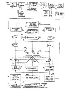
In the digital television signal receivers of FIGURES 1 - 6, digital
television
signals as received at radio frequencies by an antennz 1 (or alternatively by
a cable
connection not shown) are amplified by a radio-frequency amplifier 2 for
application
to a tirst mixer 3, to be heterodyned in the mixer 3 with first local
oscillations
generated by a first local oscillator 4. The mixer 3 translates the
frequencies of a
selected digital television signal to a~first intermediate-frequency band,
which in the
plural-conversion receiver shown in FIGURES 1 - 6 reposes in the UHF band
l S somewhat above television broadcast channel eighty-three. The first
intermediate-frequency signal thus generated by the mixer 3 is supplied to an
ultra-high-frequency-band intermediate-frequency amplifier 5, which supplies
amplified first intermediate-frequency signal to a surface-acoustic-wave (SAW)
filter
6 designed to select VSB AM DTV signals as translated to the first
intermediate-frequency band.
In a digital signal receiver there is great eoncem in carefully controlling
the
overall amplitude and phase characteristics of the receiver in order to
minimize
intersymbol error, while at the same time rejecting interference from signals
in
adjacent channels. Getting flat amplitude response within tldB over a
bandwidth of
2S S.S to 6 MHz, while maintaining acceptable group delay characteristics,
requires
SAW filtering with a great number of poles and zeroes to define the receiver
bandwidth. It is difficult and expensive to implement such SAW filtering for a
VIrF
band, such as 41 - 47 MHz. Also, the insertion loss is quite high in a VHF
band,
typically 15 - 17 dB for the 41 - 47 MHz band. The SAW filtering to define
receiver
bandwidth can be more easily implemented for a UHF band, such as at 917 - 923
8


CA 02242294 1998-07-06
MHz, as long as care is taken to drive the SAW filter from the optimal source
impedance specified by its manufacturer. This is because the df/f ratio of 6
MHz to
920 M.Hz is substantially lower than the ~f/f ratio of 6 MHz to 44 MHz.
Insertion
losses also tend to be lower in a UHF band, typically 10 - l2 dH for the 917 -
923
MHz band.
The UHF-band IF amplifier 5 provides gain to make up for the insertion loss
in the SAW tiller 6. Not controlling the gain of the amplifier ~ makes it
easier for the
amplifier ~ to drive the SAW filter b from an optimal source impedance.
Selected
amplified first intermediate-frequency signal is supplied from the SAW filter
6 to a
second mixer 7, to be heterodyned in the mixer 7 with first local oscillations
generated
by a controlled second local oscillator 8 in FIGURES 1, 2 and 5 and by a
fixed-frequency second local oscillator 08 in FIGURES 3, 4 and 6. The mixer 7
translates the frequencies of a selected digital television sisnal to a
second,
penultimate intermediate-frequency ~ba~~d, which in the plural-conversion
receivers
1 S shown in FIGURES 1 - 6 reposes in the VHF band somewhat below television
broadcast channel two. A surface-acoustic-wave (SAW) filter 9 suppresses the
image
of the second, penultimate intermediate-frequency signal generated by the
mixer 7;
and the penultimate intermediate-frequency signal is then amplified by a
very-high-frequency-band intermediate-frequency amplifier 10. This VHF-band IF
amplifier 10 is provided with automatic gain control (AGC), and the RF
amplifier is
provided with delayed AGC. So, the amplified penultimate intenmediate-
frequency
signal from the V1~F-band IF amplitier 10 is of a prescribed amplitude for
application
to mixers 11 and 12 of switching type.
In the digital signal receivers of FIGURES t - 4, designed for receiving VSH
AM DTV signals accompanied by a pilot carrier, AGC is preferably generated in
response to the amplitude of the pilot carrier, as described by C. H. Patel
and A. L. R.
Limberg in U. S, patent No. 5,636,252 issued 3 June 1997 and entitled
"AUTOMATIC GAIN CONTROL OF RADIO RECEIVER FOR RECEIVING
DIGITAL HIGH-DEFINITION TELEVISION SIGNALS". In the digital signal
receivers of FIGURES S and 6, designed for receiving QAM DTV signals
unaccompanied by a pilot carrier, AGC can be generated in any one of a number
of
9


CA 02242294 2000-11-O1
ways. T. M. Wagner er alii in >J. S. patent No. 5,235,424 issued 10 August
1993,
entitled AUTOMATIC GAIN CONTROL SYSTEM FOR A HIGH
DEFINITION TELEVISION RECEIVER, describes
taking the square root of the sums of the squares of the real and imaginary
samples of the QAM signals to develop AGC signals. In effect, this is a
digital
method for detecting the envelope of the QAM signal.
In each of the DT'V signal receivers of FIGURES 1 - 6, the mixers 11 and 12
heterodyne the penultimate IF signal to generate real and imaginary components
of an
ultimate intermediate-frequency signal falling in a 6-MHz-wide frequency band
offset
from zero frequency by at most a few MHz. The real component of the ultimate
intermediate-frequency signal.in the mixer 11 output signal is separated from
its
image by a lowpass filter 13 for applicutio.n to an analog-to-digital
converter 14; and
the imaginary component of the ultimate intermediate-frequency signal in the
mixer
12 output signal is separated from its image by a lowpass filter 15 for
application to
1 S an analog-to-digital converter 16.
In the DTV signal receivers of FIGURES 1 and Z, switching in the mixer 11 is
controlled by third local oscillations applied thereto without appreciable
phase shift
from a third local oscillator 17, and switching in the mixer 12 is controlled
by third
local oscillations phase shifted 90° by a phase shift network 18. The
third local
oscillations are supplied without appreciable phase fitter at fixed-frequency
by the
third local oscillator 17, which is advantageously a crystal-controlled
oscillator.
In the FIGURE 1 DTV signal receiver a synchronous detector 20 implements a
synchrodyning procedure for developing quadrature-phase baseband signal from
which automatic frequency and phase control (AFPC) signal is developed for the
controlled second local oscillator 8. The synchronous detector ZO comprises
digital
multipliers Z1 and 22, receiving digital samples o.f the real and imaginary
components
of ultimate IF signal cagier as their respective multiplier signals. The
synchronous
detector 20 further comprises a digital subtractor Z3 which differentially
combines the
product output signals from the in multipliers 21 and 2Z to generate the
quadrature-phase baseband signal that the synchronous detector 20 supplies as
its
LO


CA 02242294 1998-07-06
output signal. The responses of narrowband bandpass digital filters 19 and 29
are
applied as multiplicand signals to digital multipliers 21 and 22,
respectively. The
filters 19 and 29 are of linear-phase finite-impulse-response (FIR) type. The
filters 19
and 29 select real and imaginary components of the pilot carrier as translated
to the
ultimate 1F band, the selections being made from real and imaginary components
of
the digitized ultimate IF signal supplied from the DACs 14 and 16. The
difference
output signal from subtractor 23 is narrow in bandwidth owing to the
narrowband
pilot-carzier-extraction filtering by the bandpass digital filters 19 and 20.
The
differwce signal from the subtractor 23, which is supplied as the synchronous
detector 20 output signal, is converted to analog form by digital-to-analog
converter
24 and is then lowpass filtered by an AFDC filter 25 to generate AFDC signal
for the
controlled second local oscillator 8.
head-only memories 26 and 27 respectively store a cosine look-up table and a
sine look-up table for digitized ultimate IF signal carrier. The ROMs 26 and
27
receive input address from a sample counter in sampling control circuitry 30,
the
operation of which sample counter will be explained in detail further on in
this
specification, with reference to FIGURE of the drawing. The ROM 26 stores a
cosine
look-up table for digitized ultimate IF signal carrier, and the ROM 27 stores
a sine
look-up table for the digitized ultimate IF signal carrier. The ROMs 26 and 27
supply
the digital samples of the real and imaginary components of ultimate IF signal
carrier
applied to the digital multipliers 21 and 22 as their respective multiplier
signals. The
ROMs 26 and 27 operate in the digital regime as an ultimate, or final, local
oscillator.
The FIGURE 2 DTV signal receiver differs from that of FIGURE 1 in the way
that AFPC signal is developed for the controlled second local oscillator 8.
The
synchronous detector 20 receives the real and imaginary components of the
digitized
ultimate IF signal directly from the DACs 14 and 16, respectively, without
narrowband pilot-carrier-extraction filtering by the bandpass digital filters
19 and 20.
Wideband operation ofthe synchronous detector 20 makes its output signal
suitable
for the extraction of symbol frequency therefrom. Accordingly, the synchronous
detector 20 output signal is supplied via a connection 28 to the sampling
control
circuitry 30 where extraction of symbol frequency is performed.


CA 02242294 1998-07-06
In the DTV signal receivers of FIGURIrS 1 - 4 a synchronous detector 40 is
implements a synchrodynirig procedure for developing in-phase baseband signal.
The
synchronous detector 40 comprises digital multipliers 41 and 42, receiving
real and
imaginary components of the digitized ultimate IF signal supplied from the
DACs 14
and 16 as their respective multiplicand signals. The synchronous detector 40
further
comprises a digital adder 43 which additively combines the pxoduct output
signals
from the multipliers 41 and 42 to generate the in-phase baseband signal that
the
synchronous detector 40 supplies as its output signal. The digital samples of
the real
and imaginary components of ultimate IF signal supplied by the ROMs 26 and 27
are
applied to the digital multipliers 42 and 41 as their respective multiplier
signals, for
implementing the synchrodyning procedure for developing the in-phase baseband
signal.
The synchronous detector 40 supplies the in-phase baseband signal to an
equalizer 44. FIGURES 1 - 4 show the equalizer 44 as constituting the complete
I S spectrum filter before symbol decoding; however, the complete spectrum
filter can
include other digital filter elements, notably a comb filter for suppressing
artifacts of
NTSC co-channel interference. A data de-interleaves 45 commutates the
equalizer 44
response into parallel streams for application to trellis decoder circuitry
46. The trellis
decoder circuitry 46 conventionally uses twelve trellis decoders. The trellis
decoding
results are supplied from the trellis decoder circuitry 4b to a byte assembler
47 that
converts the trellis decoder circuitry 46 output signals into bytes ofReod-
Solomon
error-correction codins for application to Reed-Solomon decoder circuitry 48,
which
perfotztls Reed-Solomon decoding to generate an error-corrected byte stream.
As in
the DTV receivers used for field testing the ATSC Digital Television Standard,
the
error-corrected bytes are supplied to a data de-randomizer (not shown) and the
remainder of the receiver (also not shown).
Wideband operation of the synchronous detector 40 makes its output signal
suitable for the extraction of symbol frequency therefrom. Accordingly, in the
DTV
signal receivers of FIGURES 1 and 3, synchronous detector 40 output signal is
supplied via a connection 49 to the sampling control circuitry 30, wherein
extraction
of symbol frequency is performed. In the DTV signal receivers of FIGURES 1 and
3
12


CA 02242294 1998-07-06
the latency or delay through the digital bandpass filters 19 and 29 must be
compensated for in the connections from the ADCs 14 and 16 to the multipliers
41
and 42 in order that the same cosine and sine look-up tables can be used for
supplying
multiplier signals to the multipliers 42 and 41 in the synchronous detector 40
as for
supplying multiplier signals to the multipliers 21 and 22 in the synchronous
detector
Z0. These compensatory delays can be provided using portions of tapped, delay
lines
also used in implementing the bandpass filters 19 and 29.
The DTV signal receivers of FIGURES 3 and 4 differ from those of FIGURES
1 and 2 in that the controlled second local oscillator 8 is replaced by n
second local
oscillator 08 of fixed-frequency type, which advantageously is a crystal-
controlled
oscillator. The DTV signal receivers of FIGURES 3 and 4 ditTer further from
those of
FIGURES 1 and ? in that the AFPC'd third local oscillator 17 of fixed-
frequency type
is dispensed with together with the associated 90° phase shift network
1.8.
Penultimate local oscillations in 0° and 90° phasings are
supplied instead by
frequency-dividing the oscillations of a controlled oscillator 50 in plural-
output
frequency dividing circuitry S1. The controlled oscillator 50 receives AFPC
signal
from the AFPC filter 26. Otherwise, the DTV signal receiver of FIGURE 3 is
similar
in construction to the DTV signal receiver of FIGURE l, and the DTV signal
receiver
of FIGURE 4 is similar in construction to the DTV signal receiver of FIGURE 2.
The digital signal receivers of FIGURES 5 and 6, designed for receiving QAM
DTV signals unaccompanied by a pilot carrier, generally resemble the digital
signal
receivers of FIGURES 2 and 4, designed for receiving VSB AM DTV signals
accompanied by a pilot carrier. In the FIGURE 5 receiver AFDC signal for the
controlled second local oscillator 8 is developed by Costar loop method. A'
digital
multiplier 52 multiplies the quadrature-phase baseband response of the
synchronous
detector 20 by the in-phase baseband response of the synchronous detector 40,
with
the resulting product being supplied to the DAC 24 as its input signal. The
AFPC
filter 25 applies the direct component and lower-frequency alternating
components of
the DAC 14 output signal to the controlled second local oscillator 8 as AFPC
signal.
The FIGURE 6 receiver employs the Costas loop method to develop AFPC signal
for
the controlled oscillator 50. The digital multiplier 52 multiplies the
quadrature-phase
13


CA 02242294 1998-07-06
baseband response of the synchronous detector 20 by the in-phase baseband
response
of the synchronous detector 40, with the resulting product being supplied to
the DAC
24 as its input signal. The AFPC filter 25 applies the direct component and
the
lower-frequency alternating components of the DAC 24 output signal to the
controlled
oscillator 50 as AFDC signal.
In the digital signal receivers of FIGURES 5 and 6 elements x26, 127, 130,
x44, 145, 146, 147 and 148 are generally similar to the elements 26, 27, 30,
44, 45,
46, 47 and 48 in the digital signal receivers of FIGURES 1 - 4. The read-only
memories 126 and 127 differ from the ROMs 26 and 27 in that they store cosine
anal
sine look-up tables for a mid-channel earner wave as translated in frequency
to the
ultimate IF band, rather than storing cosine and sine look-up tables for a
carrier wave
3l0 kHz from the lower limit frequency of the TV transmission channel as
translated
in frequency to the ultimate IF band.
The sampling control circuitry 130 in FIGURES 5 and 6 receives the response
1 p of the DAC 24 to the product from the multiplier S2, to be filtered for
recovering
symbol frequency. The sampling control circuitry 130 differs in this respect
from the
sampling control circuitry 30, which receives the in-phase baseband response
from the
synchronous detector 20 or the quadrature-phase baseband response from the
synchronous detector 40 for squaring, digital-to-analog conversion and
filtering for
recovering symbol frequency.
The equalizer 144 operates on both in-phase baseband response from the
synchronous detector 20 and quadrature-phase baseband response from the
synchronous detector 40, rather than on just in-phase baseband response from
the
synchronous detector 20 per the equalizer 44 in the DTV signal receivers of
FIGURES 1 - 4. Since artifacts of NTSC co-channel interference have different
spectral characteristics in QAM DTV signal reception, the trellis decoder
circuitry 1,46
for QAM DTV signal may not operate on a 12-phase basis per the trellis decoder
circuitry 46 of FIGURES 1 - 4. In such case, the de-interleaves 145 will be of
different design than the de-interleaves 45 or will be dispensed with
altogether, and
the byte assembler 147 will be of different design than the byte assembler 47.
The
14


CA 02242294 1998-07-06
byte assembler 147 will be of different design than the byte assembler 47 also
if the
Reed-Solomon decoder circuitry x48 is of different design than the Reed-
Solomon
decoder circuitry 48.
FIGURE 7 illustrates one particular way to construct the switching mixer 11
and the lowpass filter 13 thereafter. The switching mixer 12 and the lowpass
filter 15
thereafter have construction identical to that of the switching miner 11 and
the
lowpass alter 13 thereafter. The switching mixers 1.1 and 12 are preferably
constructed within the confines of a single monolithic integrated circuit (IC)
to
facilitate such identical construction, The direct potential sources 53-~6 are
I O representative of internal voltage supply circuitry on this IC, the design
of such
internal voltage supply circuitry being well-known to analog IC designers. The
voltage bus 57 conducts the positive operating potential supplied to the IC;
and the
ground connections are to a voltage bus that conducts the negative operating
potential
supplied to the IC, which potential is applied per custom to the substrate of
the IC.
The switching mixers 11 and 12 receive penultimate IF signal input from the
same
source 58, but each has respective sources 59 and 6U of push-pull local
oscillator
signal. 1'he local oscillator signals supplied by the sources 59 and 60 in the
switching
mixer 12 are in quadrature with the local oscillator signals supplied by the
sources 59
and 60 in the switching mixer il. In each of the switching mixers 11 and 12
the
penultimate IF signal is amplified by a differential-input amplifier
comprising an
emitter-coupled pair of NpN bipolar transistors 61 and 62, a resistor 63
between the
emitters of the transistors 61 and 62, an NPN bipolar transistor 64 and its
emitter
degeneration resistor 65 connected as a constant current sink for the emitter
of
transistor 61, and an NPN bipolar transistor 66 and its emitter degeneration
resistor 67
connected as a constant current sink for the emitter of the transistor 62. The
collectors
of the transistors 61 and l2 are connected to the voltage bus 57, each
connection
alternately being a direct connection and being a connection through a mixer
output
load resistor 68. The emitter degeneration that the resistor 63 provides to
the
transistors 61 and 62 stabilizes the conversion gain of the mixer, causing it
to be fixed
in ratio to the ratio of the resistances of the resistors 68 and 63.
l5


CA 02242294 1998-07-06
More particularly, the collector of the transistor 61 connects to the joined
emitters of NPN bipolar transistors 69 and 7U, the collectors of which connect
to the
voltage bus 57 directly and through the mixer output load resistor 68,
respectively.
And the collector of the transistor G2 connects to the joined emitters of NPN
bipolar
transistors 71 and 72, the collectors of which connect to the voltage bus 57
directly
and through the mixer output load resistor 68, respectively. The source 59 of
local
oscillator signal is connected between a node 73 to which the base electrodes
of the
transistors 69 and 7Z connect and a node 74 to which the base electrodes of
the
transistors 70 and 71 connect.
When the local oscillator signals supplied from the sources 59 and GO raise
the
voltage at node 74 positive with respect to the voltage at node 73, the
transistors 69
and 72 are biased into non-conduction, and the transistors 70 and 71 are
biased into
conduction, to supply the collector current demand of the transistor 6.1 from
the
voltage bus 57 through the resistor 68, and to supply the collector current
demand of
the transistor G2 directly from the voltage bus 57. The resulting voltage
swing' across
the mixer output load resistor 68 exhibits inverting gain respective to the
penultimate
IF signal input from the source 58.
When the local oscillator signals supplied from the sources 59 and 60 raise
the
voltage at node 73 positive with respect to the voltage at node 7=t, the
transistors 70
and 71 are biased into non-conduction, and the transistors 69 and 72 are
biased into
conduction, to supply the collector current demand of the transistor 61
directly from
the voltage bus 57, and to supply the collector current demand of the
transistor 62
from the voltage bus S7 through the resistor 68. The resulting voltage swing
across
the mixer output load resistor 68 exhibits non-inverting gain respective to
the
penultimate IF signal input from the source 58.
To facilitate matching the cotl.version gains of the mixers 11 and 12, the two
switching states of each mixer should exhibit equal durations. By way of
example
this can be arranged for by differentially driving the nodes 73 and 74 from
the
center-tapped secondary winding of a tuned transformer, the primary winding of
l6


CA 02242294 1998-07-06
which receives sinusoidal local oscillations of suff cient amplitude to
guarantee 180°
duration of each switching state.
The FIGURE 7 switching mixer employs an NPN bipolar transistor 75
connected as a voltage follo~.ver for applying the signal appearing as a
voltage drop
across the mixer output load resistor G8 to the ensuing lowpass .filter for
suppressing
image signal. To maintain the source impedance from the emitter of. the
voltage
follower transistor 75 low over a full range of output signal voltage swing,
this emitter
follower transistor is provided with a shunt regulated load. The collector
current of
the transistor 75 causes a voltage drop across a collector resistor 76 thereof
, which
0 drop is applied through a voltage translation network to the base of an NPN
bipolar
transistor 77 that functions as a shunt regulator. T'he collector current
demanded by
the shunt-regulator transistor 77 from the emitter of the follower transistor
75 is
increased responsive to any tendency of the transistor 75 conduction to be
reduced,
since the drop across the resistor 76 decreases to raise the base voltage of
the
transistor 77. The voltage translation network for applying the drop voltage
across the
resistor 76 to the base electrode of the transistor 77 comprises an NPN
bipolar
transistor 78 connected as an emitter follower, a dropping resistor 79 between
transistor 78 emitter and transistor 77 base electrode, and an NPN bipolar
transistor 80
with an emitter degeneration resistor 81., which transistor 80 is connected to
demand a
constant collector current flow through the dropping resistor 79 to increase
the voltage
drop thereacross.
Keeping the source impedance from the emitter of the voltage follower
transistor 75 low over a full range of output signal voltage swing facilitates
the
lowpass filter following the mixer being a designed for "zero" source
impedance to
have a series inductor driven from the vohage follower transistor 75. Tbis
avoids
uncertainty in regard to actual resistance values in the IC having any
appreciable
effect on the lowpass filter transfer characteristic. FIGURE 7 shows the
lowpass filter
as comprising a single LC section with a series arm inductor 82, a shunt leg
capacitor
83 and a termination resistor 84. Plural-section LC filters can be used
alternatively,
of course. The lowpass filter can be of Butterworth type. The switching mixers
per
FIGURE 7 can be replaced by switching mixers of other types that exhibit
conversion
17


CA 02242294 1998-07-06
gains that are well-defined, so that a pair of switching mixers with. matching
characteristics can be constructed.
FIGURE 8 shows how a plural-phase analog-to-digital converter (ADC) is
constructed from a plurality of component ADCs of a successive binary
S approximation type. Preferably, each of the ADCs 14 and 16 in any of the DTV
signal receivers of FIGURES 1 - 6 is of. plural-phase type similar to the
other ADC.
FIGURE 8 illustrates a 24-phase ADC using a set 86 of twenty-four component
ADCs
BGA, 8GB, 86C, 86D, 86E, 86F, 86G, 86H, BGJ, 86K, 86L, 86M, 86N, 8GP, 86Q,
86R, $GS, 86T, 86U, 86V, 86W, 86X, 86Y, 86Z that sequentially and cyclically
sample an analog ultimate IF signal supplied as the response of one of the
lowpass
t-alters 13 or 15. The ADCs 86A, 86B, 86C, 86D, 86E, 86F, 86G, 86H, 86J, 86K,
8G1~, 86M, 86N, 86P, 86Q, 86R, 865, 86T, 86U, 86V, 86V1~, 86X, 86X, 86Z each
being of successive binary approximation type supply their respective output
signals
in serial-bit form; and a set 87 of serial-input/parallel-output registers
87A, 87B, 87C,
87I), 87E, $7F, 87G, 87H, 87J, 87K, 87L, 87M, 87N, 87P, 87Q, 87R, 875, 87T,
87U, 87V, 87W, 87X, 871', $7Z convert these respective output signals to
parallel-bit
form. These 24-phase parallel-bit ADC responses are supplied to an interleaver
$8
which time-division-multiplexes the response together to simulate the response
of a
single-phase flash converter.
FIGURE 8 also shows elements 89-92, as included u~ the sampling control
circuitry 30 of the DTV signal receivers of FIGURES 1 - 4 and in the sampling
control circuitry 130 of the DTV signal receivers of FIGURES 5 and 6, and as
used in
common by the ADCs 14 and 16 in those receivers. A binary counter 89 is used
for
counting samples in each of consecutive time periods, the samples occurring at
a
multiple at least two of symbol rate to meet the Nyquist criterion for
sampling without
loss of information. Each of these consecutive time periods is presumed to
have a
duration of twelve symbol epochs or a multiple thereof, so that the
customarily
12-phase operation of the trellis decoder circuitry 46 can be controlled by
decoding
the sample count from the sample counter 89 (as will be described further on
in this
specification, in detailed description of FIGURE 9 of the drawing). The number
of
phases used for analog-to-digital conversion affects the duration these
consecutive
18


CA 02242294 1998-07-06
time periods must have, so that plural-phase analog-to-digital conversion can
be
controlled by decoding the sample count from the sample counter 89. Decoding
of
the sample count from the sample counter 89 is used to determine the timing
and
duration of the input sample taken in each phase of analog-to-digital
conversion, and
the successive binary approximations by each component ADC of the plural-phase
analog-to-digital conversion circuitry is timed in accordance with the count
conditions
in the sample counter 89. The rate at which successive binary approximations
are
made can be lower than the input sampling rate, if the number of conversion
phases is
sufficiently large.
The preference for 24-phase analog-to-digital conversion at a rate twice
symbol rate is partially founded on the fact that the time period over which
the sample
counter 89 reaches full count can then have a duration of only twelve symbol
epochs,
in addition to the fact that twelve or more bits of ADC resolution can be
achieved at
successive approximation rates that are the same as symbol rate. Twelve-phase
analog-to-digital conversion at a rate twice symbol rate can be easily
controlled by
decoding the sample count from the sample counter 89 designed to reach full
count
over a duration of twelve symbol epochs. This can be achieved with a
successive
approximation rate that is the same as symbol rate, providing ADC bit-
resolution
requirements ate eleven bits or less. ~Tigher bit resolution practically
requires
successive approximation rates that are twice symbol rate, which increases ADC
power consumption almost four-fold. Doubling the.number of conversion phases
to
twenty-four, while keeping the successive approximation rate the same as
symbol
rate, substantially doubles overall ADC power consumption, rather than
quadrupling
it.
Sixteen-phase analog-to-digital conversion at a rate twice symbol rate, with
successive approximation rate that is the same as symbol rate, is a possible
consideration. Such 16-phase analog-to-digital conversion facilitated by the
sample
counter 89 being designed to reach full count over a duration of forty-eight
symbol
epochs, rather than just twelve symbol epochs. The savings in ADC hardware and
power consumption may justify the increased complexity of the decoders used
for
timing ADC operation.
19


CA 02242294 1998-07-06
Twelve-phase analog-to-digital conversion at a rate twice symbol rate, with
successive approximation late that is the same as symbol rate, can be modified
so that
less significant bits are obtained by flash conversion, rather than successive
binary
approximation. This can get bit-resolution up to twelve bits or somewhat more,
while
conserving considerable power over flash conversion alone.
In FIGURE 8 (and 9) circuitry 90 combines a symbol phase error signal with
the sample count from the sample counter 89 to generate an adjusted sample
count
used for addressing the ROMs 26 and 2'1 in the DTV signal receivers of FIGURES
1 -
4. A method similar to that S. U. H. Qureshi describes for use with pulse
amplitude
modulation (PAM) signals in his paper "'timing Recovery for Equalized Partial-
Response Systems", IEEE Transactions on Communications, December 1976,
pp.1326-1330 can be used to generate the symbol phase error signals from the
equalizer 44 response in the DTV signal receivers of FIGURES 1 - 4
Alternatively, in FIGURE 8 (and 10) circuitry 190 combines a symbol phase
t5 error signal with the sample count from the sample counter 89 to generate
an adjusted
sample count used for addressing the ROMs 126 and 127 in the DTV signal
receivers
of FIGURES 5 and 6. U. S. patent No. 5,115,454 issued 19 May 1992 to A. D.
~,Kucar,
entitled "METHOD AND APPARATUS FOR CARRIER SYNCHRONIZATION
AND DATA DETECTION" describes several types of symbol-clock-rotation detector
suitable for use in QAM DTV signal receivers and catalogues background
literature
describing certain of these types of detector. A particular one 195 of these
symbol-clock-rotation detectors can be arranged in either of the DTV signal
receivers
of FIGURES 5 and 6 to generate symbol phase error signal responsive to
equalizer
144 response.
In FIGURE 8 a bank 91 of decoders responds to various values of sample
count from the counter 89 for timing the consecutive input sampling times of
the
ADCs 86A, 86H, 86C, 86D, 86E, 86F, 86G, 86H, 86,f, 86K, 86L, 86M, 86N, 86P,
86Q, 86R, 865, 86T, 86U, 86V, 86W, 86X, 86Y, 86Z. 'the toggling of a less
significant bit from one of the stages in the counter 89 clocks the successive
binary
approximation procedures in each of these ADCs and their serial loading of the
serial-
zo


CA 02242294 1998-07-06
in/parallel-out registers 87A, 87B, 87C, 87n, 87E, 87F, 87G, 87H, 87J, 87K,
87L,
87M, 87N, 87P, 87Q, 87R, 87S, 87T, 87U, 87V, 87W, 87X, $7Y, 87Z these ADCs
respectively supply serial-bit input signals to. A bank 92 of decoders
responds to
various values of sample count from the counter 89 for controlling the
successive
polling of the SIPO registers 87A, 87B, 87C, 87D, 87E, 87F, 8?G, 87H, 87J,
8710,
87L, 87M', 87N, 87P, 87Q, 87R, 87S, 87T, 87U, 87V, 87W, 87X, 87Y, 87Z contents
by the interleaver 88 to time-division-multiplex the 24-phase ADC results for
generating digital ultimate IF signal.
In the case of the ADC 14 this digital ultimate IF signal is applied to the
digital multipliers 21 and 41; in the case of the ADC 16 this digital ultimate
IF signal
is applied to the digital multipliers 22 and 42. Since the interleaver 88
time-division-multiplex output signal is composed of parallel-bit digital
samples, the
digital multipliers 21, 22, 41 and 42 are best implemented as read-only
mern.ories, to
accommodate the high sample throughput rate.
1 S In alternative embodiments of the invention, the single-phase
multiplication
procedures implemented by the multipliers 21, 22, 41 and 42 can be replaced by
24-phase multiplication procedures in which each multiplier phase includes a
digital
multiplier receiving serial-bit input from a respective one of the ADCs 86A,
86B,
86C, 86n, 86E, 86F, 86G, 86H, 86J, 86K, 86L, 86M, 86N, 86P, 86Q, 86R, 865,
86T, 86U, 86V, 86W, 86X, 86Y, 86Z as multiplier signal for multiplying with a
multiplicand signal loaded to an icand register from one of the digital
carrier ROMs
26, 27, 126, 127. Serial-bit to parallel-bit conversion by the serial-
inlparallel-out
registers 87A, 87B, 87C, 87D, 87E, 87F, 87G, 87H, 87J, 87K, 87L, 87M, 87N,
87P,
87Q, 87R, 87S, 87T, 87U, 87'V, 87W, 87X, 87Y, 87Z would then be deferred to
take
place after 24-phase subtraction by a modified subtractor 23 or after 24-phase
addition
by a modified adder 43. This halves the number of serial-in/parallel-out
registers
required as compared to the embodiments of the invention previously described.
Multiplications by logical computation proceed at a rate one-twenty-fourth as
fast as
required for single-phase computation, saving considerable power.
21


CA 02242294 1998-07-06
FIGURE 9 shows in greater detail how in the DTV sil;nal receivers of
FIGURF_S 1 - ~~ the trellis coder circuitry 46 is implemented an a 12-phase
basis using
twelve trellis decoders 46A, 46C, 4GE, 46G, 46J, 4GL, 46N, 4GQ, 465, 46U, 46W,
4GY of a lmawn form, such as one of those described in U. S. patent No.
5,63b,251.
The trellis cod~:rs can be of a type that uses "soft" decoding, such as
described by
Viterbi, or can be of a type that uses "hard" decoding usin; data-slicers with
fixed
boundary valu a. The trellis decoders 46A, 4GC, ~16r, 46G, 46.7, 4GL, 46N,
46Q,
4GS, 46U, 4GVV, 46Y receive respective input signals from latch circuits 45A,
45C,
45C, 45G, aS,:~, 45L, 45N, 4SQ, 455, 45U, 45W, 45Y, respectively, within the
l t) de-in.terleaver 45. This set of twelve latch circuits within the de-
intcrlea er 45
consecutively and cyclically latch alternate ones of the samples at equalizer
44
response to be temporarily stored for 1?-symbol duration, thereby implementing
a ~~:1
decimation procedure. The latch carnrnands for these twelve latch. circuits
are
generated by f. bank 93 of decoders responding to appropriate values of the
sample
count supplied by the sample counter $9. The trellis decoders 46A, 46C, 46E,
46G,
4bJ, 4GL, 4Gl'f, 46Q, 465, 46U, 46W, 46Y supply their respective trellis
decoding
results to the I~yte assembler 47. The byte assembler 47 interleaves the
trellis
decoding results and builds bytes from the interleaved trellis decoding
results for
application to the error-correcting Reed-Saloman decoder circuitry 48. Polling
of
?U trellis decode results from the trellis decoders 4GA, 46C, 4GE, 46G, 4GJ,
46L, 4GN,
46Q, 4GS, 46~~:J, 4GW, 4GY .for building bytes is done by multiplexers within
the byte
assembler 47, which multiplexers are controlled by a bank 94 of decoders
responding
to appropriate values of the sample count supplied by the sample counter $9.
FIG1J~E 10 shows in greater detail how in the DTV signal receivers of
FTGUFtES 5 send 6 the trellis coder circuitry 14G is implemented an a 12-phase
basis
using twelve ~rcllls clCUUsma 1.4d~'., i~Gf?, 1.4LL~'', ldLG', 146J, HILL,
1n~111, lrltiQ,
1~46S, 14GU, 16W, .1.46Y of a known form, such as one of those described in U.
S.
patent No. S,~i36,251. The trellis coders can be of a type that uses "soft"
decoding,
such as described by Viterbi, or can be of a type that uses "hard" decoding
using
data-slicers v~ith fixed boundary values. The trellis decoders 14GA, 146C,
14G:E,
I46G, 146J, 14GL, 146N, 14GQ, 1465, 146U, 46W, 14GY receive respective input
22


CA 02242294 1998-07-06
signals from latch circuits 145A, 145C, 145E, 1456, 145J, 145L, 14~N, 145Q,
1455,
145U, 145W, 145Y, respectively, within the de-interleaves 14~. This set of
twelve
latch circuits within the de-interleaves 1.45 consecutively and cyclically
latch samples
of equalizer 144 response to be temporarily stored for I2-symbol duration. The
latch
S commands far these twelve latch circuits are generated by a bank 193 of
decoders
responding to appropriate values of the sample count supplied by the sample
counter
89. The trellis decoders 146A, 14GC, 146E, 1466, 146J, 146L, 146N, 146Q, 146S,
1.4GU, 46W, 146Y supply their respective trellis decoding results to the byte
assembler 147. The byte assembler 147 interleaves the trellis decoding results
and
builds bytes from the interleaved trellis decoding results for application to
the
error-correcting Reed-Solomon decoder circuitry 148. Polling of trellis decode
results
from the trellis decoders 146A, 146C, 14GF, 14GG,14GJ, 14GL, 146N, 146Q,1465,
146U, 46W, 146Y for building bytes is done by multiplexers within the byte
assembler 147, which multiplexers are controlled by a bank a.94 of decoders
1 S responding to appropriate values of the sample count supplied by the
sample counter
89.
The real and imaginary responses of the equalizer 144 are independently
symbol decoded in a DTV signal receiver per FIGURE 10. Alternatively, complex
symbols may be employed and, rather than one-dimensional trellis decoding
being
performed on the real component and on the imaginary component, trellis
decoding
can be carried forward on a two-dimensional basis.
FIGURE 11 shows details of how the sampling control circuitry 30 is
constructed. A master oscillator 31 oscillating at a frequency that is a
multiple of
symbol rate, as controlled in response to an automatic frequency and phase
control
(AFPC) signal, supplies its oscillations to a xero-crossing detector 32. The
zero-crossing detector 32 detects the oscillations crossing their average
value axis to
generate pulses supplied to the sample counter 89 as input signal to be
counted. The
fo«r most significant bits of the sample count are presumed to be binary-coded
modulo-12 count of symbol periods, the fourthmost significant bit toggling at
symbol
rate. This fourthmost significant bit is converted to an analog signal by a
digital-to-analog converter 33 for application as a square-wave carrier to a
23


CA 02242294 1998-07-06
synchronous detector 34 for synchrodyning an extracted symbol .frequency
signal to
baseband, thereafter to be lowpass filtered by an automatic frequency and
phase
control filter 3~ to generate AFDC signal for the master oscillator 31.
In the DTV signal receivers of FIGURES 1 - 4 the extracted symbol frequency
S signal supplied to the synchronous detector 34 is generated from the product
output
signal supplied by a digital multiplier 36. The digital multiplier 36 is
arranged to
square the baseband results of a synchrodyne procedure. Preferably, the
baseband
results of a quadrature-phase synclirodyne procedure are obtained from the
subtractor
23 for squaring by the multiplier 36, since these baseband results are
unaccompanied
by a direct component generated by detecting the pilot carrier of the DTV
signal.
Alternatively, the baseband results of an in-phase synchrodyne procedure can
be
obtained from the adder 43 for squaring by the multiplier 36. It is convenient
to
constmct the digital multiplier 36, not from logic circuitry, but rather as a
read-only
memory storing a look-up table of squaring results. A digital-to-analog
converter 37
converts the product from the digital multiplier 36 to an analog signal
supplied to a
bandpass filter 38 for extracting 10.76 MHz symbol frequency signal therefrom.
The
response of the bandpass filter 38 is supplied as locking input signal to an
injection-lock oscillator 39 with a natural oscillating frequency
substantially at I 0.76
MHz symbol frequency. The injection-lock oscillator 39 synchronizes its
oscillations
with the locking input signal and supplies a constant-amplitude extracted
symbol
frequency signal to the synchronous detector 34 to be synchrodyned to baseband
for
generating an AFPC signal to be separated by the lowpass filter 35 for
application to
the master oscillator 31.
In regard to the DTV signal receivers of FIGURES 5 and 6, the FIGURE 11
circuitry is modified, with the multiplier 36 being replaced by the digital
multiplier
52, and with the banks 93 and 94 of decoders being replaced by the banks 193
and
194 of decoders. The sample count offset con:ection circuitry 90 is modified
to a form
19U in which the symbol phase error detector 95 is replaced by a symbol phase
error
detector 19S that is, by way of exampte, one of the symbol-clock-rotation
detectors
described in U. S. patent No. 5,115,454 arranged to generate symbol phase
error
signal responsive to equalizer 144 response.
24

Representative Drawing
A single figure which represents the drawing illustrating the invention.
Administrative Status

For a clearer understanding of the status of the application/patent presented on this page, the site Disclaimer , as well as the definitions for Patent , Administrative Status , Maintenance Fee  and Payment History  should be consulted.

Administrative Status

Title Date
Forecasted Issue Date 2001-10-23
(22) Filed 1998-07-06
Examination Requested 1998-07-06
(41) Open to Public Inspection 1999-01-10
(45) Issued 2001-10-23
Deemed Expired 2009-07-06

Abandonment History

There is no abandonment history.

Payment History

Fee Type Anniversary Year Due Date Amount Paid Paid Date
Request for Examination $400.00 1998-07-06
Application Fee $300.00 1998-07-06
Registration of a document - section 124 $100.00 1999-05-06
Maintenance Fee - Application - New Act 2 2000-07-06 $100.00 2000-06-05
Maintenance Fee - Application - New Act 3 2001-07-06 $100.00 2001-07-03
Final Fee $300.00 2001-07-09
Maintenance Fee - Patent - New Act 4 2002-07-08 $100.00 2002-06-17
Maintenance Fee - Patent - New Act 5 2003-07-07 $150.00 2003-06-19
Maintenance Fee - Patent - New Act 6 2004-07-06 $200.00 2004-06-16
Maintenance Fee - Patent - New Act 7 2005-07-06 $200.00 2005-06-07
Maintenance Fee - Patent - New Act 8 2006-07-06 $200.00 2006-06-07
Maintenance Fee - Patent - New Act 9 2007-07-06 $200.00 2007-06-07
Owners on Record

Note: Records showing the ownership history in alphabetical order.

Current Owners on Record
SAMSUNG ELECTRONICS CO., LTD.
Past Owners on Record
LIMBERG, ALLEN LEROY
Past Owners that do not appear in the "Owners on Record" listing will appear in other documentation within the application.
Documents

To view selected files, please enter reCAPTCHA code :


To view images, click a link in the Document Description column. To download the documents, select one or more checkboxes in the first column and then click the "Download Selected in PDF format (Zip Archive)" or the "Download Selected as Single PDF" button.

List of published and non-published patent-specific documents on the CPD .

If you have any difficulty accessing content, you can call the Client Service Centre at 1-866-997-1936 or send them an e-mail at CIPO Client Service Centre.


Document
Description 
Date
(yyyy-mm-dd) 
Number of pages   Size of Image (KB) 
Cover Page 2001-10-03 2 58
Representative Drawing 2001-10-03 1 12
Claims 2000-11-01 32 1,576
Description 2000-11-01 24 1,154
Description 1998-07-06 24 1,153
Abstract 1998-07-06 1 29
Claims 1998-07-06 11 311
Drawings 1998-07-06 11 323
Cover Page 1999-02-03 2 92
Representative Drawing 1999-02-03 1 14
Fees 2000-06-05 1 39
Prosecution-Amendment 2000-08-01 2 42
Correspondence 2001-07-09 1 41
Prosecution-Amendment 2000-11-01 29 1,553
Assignment 1999-05-06 2 72
Fees 2001-07-03 1 41
Assignment 1998-07-06 4 121
Correspondence 1998-09-15 1 31
Prosecution Correspondence 1998-09-22 1 28