Note: Descriptions are shown in the official language in which they were submitted.
CA 02242442 1998-07-07
METHOD AND APPARATUS FOR PRODUCING POWER
FOR AN INDUCTION HEATING SYSTEM
BACKGROUND OF THE INVENTION
Technical Field
The present invention relates generally to
induction heaters and, in particular, to induction heating
systems having switchable power supplies.
Backqround Art
Induction heating is a well known method for
producing heat in a localized area on a susceptible metallic
object. Induction heating involves applying an AC electric
signal to a heating loop or coil placed near a specific
location on or around the metallic object to be heated. The
varying or alternating current in the loop creates a varying
magnetic flux within the metal to be heated. Current is
induced in the metal by the magnetic flux, thus heating it.
Induction heating may be used for many different purposes
including curing adhesives, hardening of metals, brazing,
soldering, welding and other fabrication processes in which
heat is a necessary or desirable agent or adjurant.
CA 02242442 1998-07-07
The prior art is replete with electrical or
electronic power supplies designed to be used in an
induction heating system. Many such power supplies develop
high frequency signals, generally in the kilohertz range,
for application to the work coil. Because there is
generally a frequency at which heating is most efficient
with respect to the work to be done, some prior art inverter
power supplies operate at a frequency selected to optimize
heating. Others operate at a resonant frequency a~termined
by the work piece and the output circuit. Heat intensity is
also dependent on the magnetic flux created, therefore some
prior art induction heaters control the current provided to
the heating coil, thereby attempting to control the heat
produced.
One example of the prior art representative of
induction heating system having inverters is United States
Patent No. 4,092,509, issued May 30, 1978, to Mitchell.
Another type of induction heater in which the
output is controlled by turning an inverter power supply on
and off is disclosed in the United States Patent No.
3,475,674, issued October 28, 1969, to Porterfield, et al.
Another known induction heater utilizing an inverter power
supply is described in United States Patent No. 3,816,690,
issued June 11, 1974, to Mittelmann.
Each of the above methods to control power
delivered by an induction heater either is not adjustable in
frequency and/or does not adequately control the heat or
power delivered to the workpiece by the heater. The prior
art induction heaters described in U.S. Patent Nos.
5,343,023 and 5,504,309 (assigned to the present assignee)
provide frequency control and a way to control the heat or
power delivered to the workpiece. These induction heating
systems include an induction head, a power supply, and a
controller. As used herein induction head refers to an
CA 02242442 1998-07-07
.
-3-
inductive load such as an induction coil or an induction
coil with matching transformer.
Some uses of induction heaters are to anneal, case
harden, or temper metals such as steel in the heat treating
industry. Also induction heaters are used to cure or
partially cure adhesives that have metallic particles or are
near a metallic part. During the induction heating process
a workpiece or part has one or more induction heads placed
around and/or in close proximity to the workpiece. Power 1~
then provided to the induction heads, which heat portions of
the part near the head, curing the adhesive, or annealing,
case hardening, or tempering the part.
One type of power supply used in induction heating
is a resonant or a quasi-resonant power supply. As used
herein resonant power supply refers to both resonant and
quasi-resonant power supplies. A resonant induction
heating power supply has an output tank formed by the
induction coil or induction head and a capacitor. Current
is provided to the tank from a current source and current
will circulate within the tank. The current from the
current source replenishes the energy in the tank reduced by
losses and energy transferred to the work piece. Generally,
the tank current facilitates power to the head.
It is desirable in some ways to operate induction
heaters at a high frequency output. A higher frequency
output allows the magnetic components (inductors and
transformers) to be smaller and lighter. This will make the
power supply less costly.
The induction heating power supplies described in
U.S. Patent 5,343j023 and 5,504,309 have control circuitry
that tracks the voltage of the resonant tank, and
alternately fires opposite pairs of IGBT's that comprise a
full bridge configuration as the tank voltage across the
devices transitions through zero. This is an attempt at
soft switching, but there is a delay in the control and gate
CA 02242442 1998-07-07
drive circuitry that causes a delay (1 2 ~sec e g ) from the
zero crossing until the IGsT turns on ~onsequently, when
the IGsT turns on, it hard switches into a positive value of
voltage and current, and the switching losses become large.
The losses for this sort of power supply increase
with frequency. First, as the frequency increases the
number of switching events increase. Second, as the
frequency increases the 1.2 ~sec delay becomes a larger
portion of the cycles, and the voltage into which the hard
switch is made will be higher. For example, at 10KHz the
voltage will be about 7.5% of the peak after 1.2 ~sec: At
50KHz the voltage will be about 38~ of the peak. Thus, the
switching voltage is higher and the losses are higher.
Finally, conduction losses are greater because the current
is off during the 1.2 ~sec. The peak current, and hence the
RMS current, must be higher-to compensate for the time the
current is off. Because conduction losses increase with the
square of the RMS current, the losses are greater. At
higher frequencies 1.2 ~sec is a larger portion of the
cycle, hence the problem is exacerbated. In sum, higher
frequency operation cause three problems: more loss events
(more switching), higher losses for each event, and
increased conduction losses.
Another prior art resonant power supply described
2S in Chapter 2 of a PH.D. thesis by L. Grajales of Virginia
Tech was designed to soft switch a transistor by starting
the switching process at zero crossing and then holding the
voltage or current, or both, to zero during the turning on
and turning off of the transistor. However, this typically
required holding the current and/or voltage at zero for a
length of time while the switch is turned on. If the
propagation delay when turning switches on and off is, for
example, 1.2 ~sec, this is about 2.4% of the cycle at 10KHz,
and is of little consequence. However, it is 12~ of the
3~ cycle at 5a KHz. mUs, to obtain the ~esired average current
CA 02242442 1998-07-07
the instantaneous current during the remaining 88% of the
cycles must be higher. This requires a higher peak current.
In other words, the current must be greater when the current
is non-zero to compensate for time it is held to zero (12%
at 50KHz e.g.). This means the peak current is higher,
which means the RMS current and losses will also be higher.
Thus, soft switching increased conduction losses.
Because soft switching reduces the losses at turn
on and turn off, at the expense of increased conduction loss
(as described above), it is a design trade off in the
Grajales method as to how much duty cycle may be sacrificed
in order to achieve minimum switching losses. The practical
limit occurs when the increased conduction losses exceed the
reduced switching losses.
Accordingly, it would be desirable to provide an
induction heating power supply that reduces switching losses
without a corresponding increase in conduction losses.
Preferably, this would be done by soft switching, or nearly
soft switching, the switches used in the output tank. The
soft switching will preferably be done by predicting zero
crossing and starting the firing process before zero
crossing.
The amount of energy delivered to the work piece
by the head must be adequately controlled to properly treat
the workpiece. This energy depends on, among other things,
the energy delivered to the head, the losses in the head,
and the relative position of the head to the workpiece
(which affects coupling). Some prior art controllers used
with inverter based power supplies measure the current
delivered to the head. However, in resonant or quasi-
resonant induction heaters the resonating current in the
tank should be measured.
It is also desirable to be able to determine the
tank current so that the user of the equipment knows how
much current is flowing in the head and to prevent the
CA 02242442 1998-07-07
capacitors which form the tank from being destroyed by to
much current and/or voltage. The current from the current
source replenishes the current in the tank due to losses and
energy transferred to the work piece.
However, the tank current is high, (1000 amps
e.g.) and, to accommodate such high currents, the bus bar
through which the current flows is tall, for example a
height of 6-18 inches. Thus, it is difficult to obtain
current sensing device which will fit around the bus bar.
Additionally, mechanical constraints may not allow much room
between the bus bars. Accordingly, it would be desirable to
have a device which allows current in a resonant tank used
in a induction heater to be able to be sensed.
Typically, power supply bus bars (for high current
applications) are thin metal plates. Copper bus bars that
carry high amounts of current must have the capacity to
carry the current without excessive losses (heating).
Excessive losses reduce efficiency and increase resistance,
thus further increasing losses. Generally, the reference
depth and height of the copper plate bus bar determines
losses. Thus, the current carrying capacity of a bus bar
is increased by increasing its height.
Generally, copper plates have a current carry
capacity of about 300 amps for every two inches of height at
60 Hz. However, at high frequencies, such as 50 Khz, the
capacity is only about 100 amps per two inches of height.
The reduced current capacity is largely due to changed
reference depth (which depends on frequency). Thus, prior
art 1000 amp induction heaters use a bus bar on the order of
18 inches high. This makes the case much larger than
otherwise necessary. Other prior art induction heaters use
two inch bus bars that are water cooled. This prevents over
heating, but is very inefficient since the losses still
occur: they are simply dissipated.
Thus, a bus bar for a 1000 amp induction heater
CA 02242442 1998-07-07
.
-7-
that is efficient yet a reasonable height is desirable.
SUMMARY OF THE INVENTION
According to a first aspect of the invention
an induction heating power supply includes a power circuit
having at least one switch and a power output. An output
circuit includes an induction head. The output circuit is
coupled to the power output. A controller has at least one
feedback input connected to the output circuit, and has a
control output connected to the switch. The controller
begins the switching process prior to the switch zero
crossing. In one embodiment the switch is soft switched.
The power circuit is a resonant power supply and
the output circuit includes a resonant tank in one
embodiment.
Another embodiment provides that the controller
includes a zero crossing detector coupled to the output
circuit and a frequency detector coupled to the zero
crossing detector. In one alternative the frequency
detector includes a ramp and a reset coupled to a zero
crossing detector.
Another embodiment provides that the controller
includes an output voltage detector coupled to the output
circuit. The controller includes a peak voltage detector
coupled to the output circuit in an alternative. A
comparator receives the peak voltage, the frequency signal,
and the output voltage in another alternative.
The controller includes a current feedback signal
input coupled to the output circuit in another embodiment.
An error circuit receives the current feedback signal and
produces an error output in response thereto. The error
output is provided as an input to the comparator.
According to another aspect of the invention a
resonant power supply comprises an output tank and at least
two bus bars connected to the output tank. The bus bars are
CA 02242442 1998-07-07
disposed with a gap therebetween. A coil is placed in the
gap between the bus bars, and a feedback circuit is
connected to the coil. Alternatives include a filter in the
feedback circuit, integrating the feedback circuit output,
or dividing the output by a signal dependent on the
frequency. In another embodiment the bus bars are
substantially parallel.
A third aspect of the invention is an induction
heating power supply comprising an output circuit having
first and second inputs. Two bus bars are connected to the
inputs. The bus bars are comprised of a plurality of
plates. In one alternative each plate has a capacitor
connected to it.
15BRIEF DESCRIPTION OF THE DRAWINGS
Figure 1 is a block diagram of an induction
heating system made in accordance with the present
invention;
Figure 2 is a perspective view of a bus bar and
current sensor in accordance with the present invention;
Figure 3 is a top view of a bus bar and current
sensor in accordance with the present invention;
Figure 4 is a side view of-a bus bar and current
sensor in accordance with the present invention;
25Figure 5 is a circuit diagram of the current
source of Figure 1;
Figure 6 is a circuit diagram of the H-Bridge of
Figure 1;
Figure 7 is a block diagram of the controls of
30Figure 1;
Figures 8-10 are circuit diagrams of the
controller of Figure 1; and
Figure 11 is a circuit diagram of an alternative
embodiment.
CA 02242442 1998-07-07
Other principal features and advantages of the
invention will become apparent to those skilled in the art
upon review of the following drawings, the detailed
description and the appended claims.
DETAILED DESCRIPTION OF A PREFERRED EXEMPLARY EMBODIMENT
Before explaining at least one embodiment of the
invention in detail it is to be understood that the
inventi_n is not limited in its application to the details
of construction and the arrangement of the components set
forth in the following description or illustrated in the
drawings. Other circuits may be used to implement the
inventing and the invention may be used in other
environments.
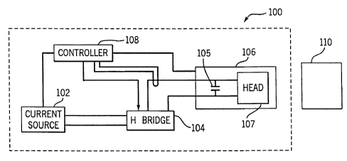
A block diagram of an induction heater 100
constructed in accordance with the preferred embodiment is
shown in Figure 1. Induction heater 100 includes a current
source 102, an H-Bridge circuit 104, an output tank 106, and
a controller 108. Output tank 106 includes a capacitance
105 (which may be implemented by multiple capacitors) and an
induction head 107. Induction head 107 is disposed near a
workpiece 110.
Current source 102 provides current to H-Bridge
104. H-Bridge 104 provides current to output tank 106. The
tank current circulates in capacitor 105 and induction head
107. The tank current in head 107 induces eddy currents in
workpiece 110, thereby heating workpiece 110.
H-Bridge 104 resonates at a frequency dependent
upon the load (size, shape, material and location of the
workpiece e.g.) and the components of induction heater 100.
The resonant frequency ranges from 10KHz to 50KHz in the
preferred embodiment.
Controller 108 receives feedback signals that
allow it to control the switches of H-Bridge 104 so that
they are switched at zero volts. Controller 108 compensates
CA 02242442 1998-07-07
-10-
for propagation delays in the logic and firing circuits by
predicting when the zero crossing will occur. Specifically,
controller 108 begins the firing or switchin~ process about
1.2 microseconds before zero crossing in the preferred
embodiment. The switching process includes the events that
occur during the propagation delay.
Controller 108 predicts or anticipates the zero
crossing using peak tank voltage, time since the previous
zero crossing, ~erage tank current and instantaneous tank
current. Also controller 108 may control current source
102. The circuitry that anticipates the zero crossing will
be described belcw. Induction heater 100 includes a bus bar
that is small yet efficient. A current sensor cooperates
with the bus bar to provide a tank current feedback signal.
Referring now to Figures 2-4 an arrangement which
allows the current in the output tank 106 to be sensed as
shown. A pair of substantially parallel copper bus bars 201
and 202 are arranged in a parallel fashion. Bus bar 202 is
attached to capacitance 105 (which is 3 capacitors 105A-105C
in the preferred embodiment). A coil 203 is placed between
bus bars 201 and 202. Coil 203 has a width substantially
equal to (slightly less than) the separation between bus
bars 201 and 202.
Alternative embodiments entail a narrower coil
than the distance between bus bars 201 and 202. Coil 203
is placed such that current from each of capacitors 105 will
flow past the coil, thereby inducing voltage in the coil.
Specifically, coil 203 is placed near the end of bus bars
201 and 202 that are attached to connectors 301 and 302
(Figure 3). All current flowing into the bus flows through
connectors 301 and 302, and thus past coil 203.
Coil 203 is connected to a resistor 205 and a
capacitor 206. The voltage on coil 203 is proportional to
the current which flows in bus bars 201 and 202 (as will be
described in detail below). An op amp 208 is connected
CA 02242442 1998-07-07
between the node common to resistor 205 and capacitor 206.
Op amp 208 is configured to be a unity gain voltage
follower, which isolates the voltage at the node common to
resistor 205 and capacitor 206. Resistor 205, capacitor 206
and op amp 208 may be located on the control board talthough
they do not need to be). Thus, the output voltage of the
filter is proportional to the tank current.
Coil 203 operates as follows: When current flows
in the parallel plates that are bus bars 201 and 202 the
current induces a magnetic field between the plates. The
magnitude of the magnetic field is proportional to the
current (assuming the dimensions the plates are much greater
than the separation of the plates). Using known equations
such as B=~o*Io, or the Biot-Savart law, the magnetic field
may be calculated. The magnetic flux ~ created by B can be
given by, ~ = B-dS.
For a coil of simple geometry inserted between the
current carrying plates and oriented along the induced
magnetic field, the flux in the coil is given by, ~=~o*Io*A,
where A = vector normal to the cross-sectional area of the
coil with magnitude equal to the area of the coil. Current
flowing in the coil is time varying and it will induce a
time varying magnetic field. Therefore, from Faraday's Law
of Induction, a voltage will be induced in the coil with a
value of: E = -d~/dt. Taking the Fourier transform shows
that the voltage induced in the coil is proportional to the
current flowing in the plates and the frequency at which the
current is alternating.
The frequency dependence can be removed by
integrating, using a low-pass filter or dividing the signal
from the coil by a signal proportional in amplitude to the
frequency of the current flowing in the plates. The filter
of Figure 2 is used in the preferred embodiment. Thus, the
output voltage of the filter is proportional to the tank
current. This method of obtaining the tank current can be
CA 02242442 1998-07-07
extended to other geometries besides parallel plates by
determining the magnetic field between the two current
carrying conductors. Other geometries can be used by an
analytical solution of the equations, computer simulation or
calibration of the actual hardware used (i.e. empirical
testing).
Bus bars 201 and 202 are comprised of three
plates, 211-216 (Figures 2-4) in the preferred embodiment.
Each plate carries one-third of tht total current. Using
three plates allows the bus bar to be relatively short
(about 6 inches in the preferred embodiment) and do not need
water cooling.
Plate 215 is connected to and carries the current
from capacitor 105A. Plate 214 is connected to and carries
the current from capacitor 105B. Plàte 213 is connected to
and carries the current from capacitor 105C. Plates 213-215
are connected to connecter 302. Thus, each plate carries
1/3 of the total current, and the height of each plate is
1/3 of the height of a single plate having the combined
-current capacity of the three plates. A similar arrangement
is used with plates 211-213. This arrangement avoids
excessive losses (and the result needed for water cooling)
and undesirable high bus bars.
Current source 102 is shown in detail in Figure 5,
and includes an input rectifier 502 which may be connected
to a three phase power source. Input rectifier 502
preferably includes 6 diodes arranged in a typical fashion.
Input rectifier 502 is connected to an inductor 503 (0.001
H) which feeds an H bridge comprised of switches 506, 507,
508 and 509. The switches in the H bridge are preferably
IGBT's, however other switches may be used. A capacitor 504
(0.0012 F) is provided across the H bridge to filter the
voltage provided through inductor 503 from rectifier 502.
The center leg of the H bridge includes the primary windings
of a transformer 510 and an inductor 512. The secondary
CA 02242442 1998-07-07
-13-
windings of transformer 510 are connected through rectifying
diodes 519-522 to inductor 524. Capacitors 513 and 514 (1.5
~F) are provided across diodes 519 and 522, respectively.
Capacitors 513 and 514 resonate with inductor 512 in a
manner known in the art. The output current source 102 is
provided to resonant circuit 104.
H-Bridge 104 shown in detail in Figure 6 and
includes IGBT's 601-604. Each IGBT has a diode associated
therewith. IGBT's 601-604 are arranged in ~n H bridge.
Tank circuit 106, including capacitor 105 (1.5 ~F) and
induction head 107 is disposed in the center leg of the H
bridge. The H bridge is switched on and off in a known
fashion but early enough to be zero voltage switched, such
that current is provided to the tank circuit and losses are
kept low. Switches 601-604 maybe switches other than
I(;BT ' S .
Generally, the prior art compared the tank voltage
to zero volts, and began firing when the tank voltage (which
is sinusoidal) crossed zero. According to the present
invention, the process to turn IGBT' s 601-604 on begins at a
time before the tank voltage crosses zero such that after
the propagation delay the tank voltage is (or has not yet
crossed) zero.
Specifically, the present invention includes an
induction heating power supply with a resonant tank output
circuit. The resonant tank circuit is fired in such a way
as to reduce switching losses, preferably soft switching the
switches, which are IGBT ' s in the preferred embodiment. The
tank voltage is equal to the switch voltage in the
configuration of the preferred embodiment. The control
circuitry predicts when the zero crossing (i.e. zero volts
and/or current across the switch) will be, and the
transistors are turned on in anticipation of the tank
voltage (which is also the switch voltage in the preferred
embodiment) passing through zero. Thus, the transistors are
CA 02242442 1998-07-07
-1 4-
turned on, or have just turned on, when the voltage
transitions through zero, thereby providing a soft switch
(or they turn on to low voltage reducing switching losses).
Because the voltage at the turn on is zero, virtually all of
the available duty cycle may be used thereby minimizing the
peak transistor currents and conduction losses.
Reduced losses are obtained when switching at or
near zero power across the switch. Zero power across the
switch is obtained by having zero volts and/or zero current
across the switch. Zero crossing, as used herein, refers to
zero power across the switch. The configuration of the
preferred embodiment uses a tank wherein the tank voltage is
equal to the switch voltage. Thus, zero crossing for the
switch occurs when there is a tank zero crossing. Other
configurations will not have a tank voltage equal to the
switch voltage.
The present invention anticipates the zero
crossing by adding (or subtracting) an offset to the tank
voltage which corresponds to an earlier time of 1.2 ~sec.
This sealed value is used, in part, to determine the offset
from zero crossing. At a given frequency a given
percentage of the peak voltage will correspond to 1.2 ~sec.
Thus, the peak tank voltage is scaled to give an appropriate
value.
However, the frequency of the tank is not fixed,
but depends on the load. The percentage of the peak that
corresponds to 1.2 ~sec at 1OKHz corresponds to much less
time at higher frequencies (for a given peak voltage) then
at lower frequencies. Thus, the frequency is also used to
determine the offset.
The instantaneous frequency must be determined
fast enough to avoid added propagation delay. Accordingly,
the preferred embodiment uses a time measured from the last
zero-crossing, which is proportional to 1/frequency. This
value is linearly scaled, and subtracted from the scaled
CA 02242442 1998-07-07
peak value. Thus, the result is an offset that increases as
the peak voltage increases, and decreases as time increases,
(or frequency decreases).
- The tank voltage is sinusoidal (non-linear), and
the scaling of the frequency (time) feedback is linear.
Thus, an error will be introduced. Other errors result from
heating, non-linearities, etc. The error is compensated for
by a circuit which "nudges" or adjusts the offset. The
amount of adjusting may be determined empirically. The
preferred embodiment adjusts the offset sufficiently to
provide true soft switching. Alternatives include
predicting zero crossing and switching into a very low
voltage, or almost soft switching.
The offset is adjusted by comparing the
instantaneous current to the average current in the
preferred embodiment. When the instantaneous current is
excessively greater than the average current (50% e.g.) the
offset is reduced. This results in a firing that provides
the desired soft switching. Also, the prior art firing
system (i.e. begin firing at zero crossingj may be included
as a back-up so that the firing process begins no later than
at zero crossing.
Figure 7 is a block diagram of the preferred
embodiment of the firing control of the IGBT's in accordance
with the preferred embodiment. Waveform 701 represents the
voltage on tank 106. The instantaneous tank voltage is
amplified by a differential amplifier 703 and fed to a
comparator 705 (with an offset as described below).
Comparator 705 compares the voltage feedback to a value
representative of zero volts from the tank. The output of
the comparator is provided to a steering flip flop circuit
707 who's output is, in turn, provided to a gate driver 709.
The present invention provides an additional input
into comparator 705 that causes the firing process to begin
before zero crossing, so that the IGBTs are on at zero
CA 02242442 1998-07-07
.
-16-
crossing. Specifically, the voltage feedback signal is also
provided to a peak detector 711. Peak detector 711 samples
the feedback voltage, and detects the peak. The output of a
reset circuit 713 is provided to peak detector 711 after
each zero crossing and causes it to be reset.
A frequency detector 712 provides an output that
ramps up with time, at a constant slope. The ramp is reset
by reset circuit 713 at each zero crossing. Thus, the
output of frequency detector 712 is proportional to the
length of time since the last zero crossing, or 1/f of the
tank voltage. Both of these signals (from peak detector 711
and from frequency detector 712) are provided to a summing
circuit 716. The frequency and peak signals are combined to
form the offset (from zero crossing) which is adjusted by an
error circuit 720.
A feedback signal indicative of the average of the
tank current is provided by average current circuit 718 to
error circuit 720. Also! a signal indicative of
instantaneous current is provided by a current circuit 719
to error circuit 720. The current feedback signals are
obtained using a current transformer measuring the current
provides by current source 102 (not the tank current).
Error circuit 720 provides a signal based upon the
current feedback to summing circuit 716 and adjusts the
offset. The output of summing circuit 716 offsets the tank
voltage signal at which the firing of the IGBT's begins
about 1.2 ~sec before zero-crossing.
The voltage is monitored in the preferred
embodiment by a circuit that tracks the voltage in the
resonant tank and feeds the peak and zero crossing
detectors. When a zero crossing is detected, the reset
circuit releases the peak detector and frequency detector
circuits. As the voltage tracks to its maximum amplitude,
the peak detector tracks along with it. When the peak is
CA 02242442 1998 - 07 - 07
attained, a diode holds the voltage level on the capacitor
at the level until it is reset.
The frequency detector circuit consists primarily
of a current source feeding a capacitor and a field effect
transistor (FET) for reset in the preferred embodiment.
When the reset is released, the current source begins
charging the capacitor in a linear fashion; therefore the
voltage across the capacitor is directly proportional to the
length of time the capacitor has been charging. Since the
time is equal to 1/ frequency, the voltage is also
proportional to frequency.
The two voltages are scaled and then summed with
the tank voltage feedback signal as described above. As the
sum passes through the zero threshold, the comparator
changes state causing the timer to deliver a pulse to the
gate drive circuitry.
After the tank voltage passes through zero, the
zero crossing detector changes state and turns on the reset
of the FETs. The voltage levels of the peak detector and
frequency are held at zero until the next zero crossing
causes the FETs to be turned off and the cycle starts over.
The detailed circuitry which implements the
preferred embodiment is shown on Figures 8-10. As one
skilled in the art will readily recognize other circuitry
may be used to implement these control functions, including
other analog or digital circuits.
The voltage feedback signal from tank 106 is
provided as VFB (Figure 8). VFB is provided to an op amp
801 which includes feedback resistors 802 (10K ohm) and 803
(1OK ohm). Op amp 801 is configured to scale the voltage
feedback signal, and is part of amplifier 703. The output
of output op amp 803 is provided to comparator 705.
The output of op amp 801 is also provided to peak
detector 711. Peak Detector 711 includes a diode 807 and a
resistor 808 (100 ohms), through which VFB is provided to a
CA 02242442 l998-07-07
-18-
unity gain op amp 810. The voltage feedback signal is also
provided through resistor 808 to a capacitor 811 (0.001~f),
and the peak of the voltage signal is held by capacitor 811.
Thus, the output of op amp 810 corresponds to the tank
voltage peak.
A switch 813 is connected in parallel with
capacitor 811 and has its gate connected to reset circuit
713. Reset circuit 713 causes switch 813 to turn on,
shorting capacitor 811 at zero crossing. Thus, sample and
hold circuit 711 samples the feedback voltage signal,
detects the peak, and stores that peak. The output of op
amp 810 (the peak tank voltage) is provided to summing
circuit 716.
Frequency detector 712 includes a pair of
transistors 820 and 821. Transistors 820 and 821 are
connected to a +15 volt supply through a pair of resistors
822 and 823 (47.5 ohms). The gates of transistor 820 and
821 are connected through a resistor 824 (30.1K ohms) to
ground. The output of transistor 821 is connected to a
capacitor 825 (0.0022 microfarad). The voltage on capacitor
825 will depend upon the length of time it has been
charging.
A switch 826 is provided in parallel with
capacitor 825 and is used to short capacitor 825. The gate
of transistor 826 is connected to reset circuit 713 and upon
a reset signal (triggered by a zero crossing) switch 826
will be turned on, and capacitor 825 will be short
circuited, and thus its voltage will be reset to zero.
Thereafter, the voltage will continue to increase
until the next resetting. The voltage on capacitor 825 is
thus proportional to the length of time between zero
crossings, and thus proportional to 1/f. The output of
capacitor 825 is provided through a resistor 827 (1K ohm) to
an inverting op amp 830. Inverting op amp 830 includes
feedback resistors 828 and 829 (1 OOK ohms). Thus, the
CA 02242442 l998-07-07
_19_
output of op amp 830 is a negative voltage proportional to
1/f of the tank circuit. The output of op amp 830 iS
provided to summing circuit 716.
Average current circuit 71 8, instantaneous current
circuit 719 and error circuit 720 are shown in Figure 9. A
feedback current signal IFB iS provided to the average
current circuit 718 which includes and op amp 901 (which
buffers and inverts the current feedback signal). The
output of op amp 901 is provided through a resistor 902 (1K
ohm) to a parallel combination of a resistor 903 (11.1K ohm)
and a capacitor 904 (10 microfarad). Resistor 903 and 904
are also connected to ground and the output of capacitor 904
represents the average current (averaged over about 100
cycles as set by the RC time constant). The output of
capacitor 904 is provided to an op amp 906 through a
resistor 905 (2OK ohm) and a feedback resistor 907 (20 K
ohm). Thus, the output of op amp 906 corresponds to the
average dc current.
A signal indicative of the tank instantaneous
current, ITANK, is provided through a resistor 910 (2k ohm)
and a diode 911 (which protects the ITANK signal) to a
comparator 912. The average dc current is also provided
through a resistor 913 (2K ohm) to comparator 912. A
negative 15 volt signal (current source) is provided through
a resistor 915 (100K ohm). Also, comparator 912 has on its
inputs a pair of diodes 916 and 917 which protect the inputs
to comparator 912. Comparator 912 is configured to provide
a high output when the instantaneous DC current exceeds the
average DC current by more than 50~.
A +15 voltage source and resistors 918 (2K ohm)
provide current to comparator 912. The output of comparator
912 is provided to the gates of a pair of transistors 920
and 921. Transistors 920 and 921 are connected to a 15 volt
supply. The common junction of transistors 920 and 921 is
provided through a diode 923 and a resistor 924 (1K ohm) to
CA 02242442 1998-07-07
-20-
a capacitor 926 (0.1 microfarad). A resistor 925 (1OOK
ohm) is provided in parallel a with capacitor 926 and both
are connected to ground at one end. Thus, when transistors
920 and 921 are turned on by comparator 912, current is
provided to capacitor 926, which integrates that current.
The current is provided when the instantaneous current
exceeds the average current by more than 50~. The output of
capacitor 926 is provided through a resistor 930 (1OOk ohm)
'o an op amp 931. Op amp 931 also receives the dc current
signal through a resistor 933 (100K ohms). Op amp 931
includes a feedback resistor 932 (100K ohm). The output of
cp amp 931 is provided to summing circuit 716.
Error circuit 720 is a circuit which adjusts by
small amounts the threshold set in response to the frequency
and peak voltage. Thus, the output of current circuit 720
is provided to summing circuit 716 along with the peak
voltage and frequencies.
Summing circuit 716 includes a resistor 951 (16.2K
ohms) connected to peak detector 711, a resistor 952 (43.2K
ohm) connected to frequency detector 712, and a resistor 953
(20K ohm) connected to error circuit 720 (Figure 8). Each
of these resistors, in turn, is connected to an op amp 955,
which includes a feedback resistor 956 (10K ohm). Op amp
955 and the associated resistors serve to scale and sum the
various feedback signals. The output of op amp 955 is the
adjusted offset to the tank voltage, and provided to
comparator 705.
The output of summing circuit 716 is provided
through a resistor 1001 (10K ohms) to a summing comparator
1012, which are part of comparator 705. The voltage
feedback signal is provided through a resistor 1003 (12.1K
ohms) also to comparator 1012. Comparator 1012 is
configured as a summing comparator and includes a capacitor
1010 (100 picofarads) and a resistor 1014 (498k ohm) that
adds hysteresis. A diode 1006 and a diode 1007 hold the
CA 02242442 l998-07-07
-21 -
inputs of comparator 1012 to acceptable levels. A capacitor
1005 (47 picofarads) filters the various inputs to
comparator 1012. The output of comparator 705 is provided
to steering flip flop circuit 707, which operates in a
conventional manner.
Steering flip flop 707 selects the earlier of the
prior art zero crossing detection or the inventive
prediction of zero crossing. The IGBT's are turned on at
the earliest of the two. Thus, in the event the prediction
circuit fails to operate properly, the control reverts to
~he prior art type of control.
Aiternative embodiments include predicting the
zero crossing by firing a preset or determined amount of
time after the previous zero crossing. Even though this is
firing after a previous zero crossing, it is still before
(and thus predicting) the next zero crossing. The time can
be determined using average or instantaneous frequency, or
by adjusting the time based on a previous error. Another
alternative uses a fixed threshold to find a "prior-to-zero"
crossing, and firing at that time. This method also
predicts the zero crossing. Also, the RMS voltage could be
used instead of the peak voltage to predict zero crossing.
Another alternative is shown in Figure 11. One of
the IGBT's, 601, from the H-Bridge is shown (without an
anti-parallel diode). A switch 1101, such as an FET, is in
parallel with switch 601. Switch 1101 is a very fast (100
nsec., e.g.), lower (than switch 601) amperage switch.
Switch 1101 is fired such that when switch 601 begins to
turn on, switch 1101 is already on and holds the voltage
across switch 1101 to close to zero. Thus, switch 601 is
soft switched. Because switch 1101 is very fast it may be
fired at zero crossing with very little loss.
Alternatively, switch 1101 may be predictively fired in
accordance with the prediction techniques described above.
CA 02242442 1998-07-07
Another alternative is to fire switches 601 and 1101
together. Again switch 1101 turns on quickly, holding the
voltage across switch 601 close to zero, thus~providing a
soft switch. After switch 601 is on, switch 1101 is turned
off. Switch 1101 carries very little current and switches
into low voltage since it is so fast. For example, a 100
nsec switching time is only one percent of a half-cycle at
5OkHz
Each of ~he embodiments described above may be
carried out using a dual arrangement (a voltage source and
firing on zero current crossing e.g.).
Thus, the present invention includes an induction
heating power supply with a resonant tank output circuit.
The resonant tank circuit is fired in such a way as to
reduce switching losses, preferably soft switching the
switches, which are IGBT's in the preferred embodiment. The
control circuitry predicts when the zero crossing (i.e. zero
volts and/or current across the switch) will be, and the
transistors are turned on in anticipation of the tank
voltage passing through zero. Thus, the transistors are
already on when the voltage transitions through zero thereby
providing a soft switch (or they turn on to low voltage
reducing switching losses). Because the voltage at the turn
on is zero virtually all of the available duty cycle may be
used, thereby minimizing the peak transistor currents and
conduction losses.
Thus, it may be seen that the present invention
as described provides a method and apparatus to provide
power for induction heating, and the power circuit is soft
switched to reduce switching losses. Also, a bus bar that
reduces size and losses is provided. A current feedback
circuit is used to determine the tank voltage.
The invention is capable of other embodiments or
being practiced or carried out in various ways, and it
should be understood that the preferred embodiments are but
CA 02242442 1998-07-07
one of many embodiments. Also, it is to be understood that
the phraseology and terminology employed herein is for the
purposes of description and should not be regarded as
limiting.