Note: Descriptions are shown in the official language in which they were submitted.
CA 02242724 1998-07-09
CA9-98-017
ADAPTIVE BANDWIDTH STABILIZATION FOR AN INTEGRATED CIRCUIT
AMPLIFIER
Field of the Invention
This invention relates to integrated circuit amplifiers having compensation
for bandwidth
stabilization over a wide range of operating supply voltages, and to
integrated circuit infrared
receivers embodying such amplifiers.
Background of the Invention
With the increasing movement of solid state electronics from discrete
component usage to integrated
circuitry, such as ASICs (Application Specific Integrated Circuits),
advantages have been gained in
l0 miniaturization, but certain limitations have been encountered as well. In
prior art, amplification
systems were built with discrete components such as capacitors and resistors
being used in
conjunction with high gain integrated circuit amplifiers to produce various
amplifier configurations
such as transconductance amplifiers. The intrinsic properties of the external
components as a
function ofthe operating voltage being used was seldom a problem, ifthe
components were not used
outside of their design voltage limitations.
The same is not necessarily the case for fully integrated circuit amplifiers
where devices such as
capacitors are integrated onto the same substrate as the amplifier. While the
various methods of
integrating capacitive devices is well known to those skilled in the art, it
is also known that the
parasitic capacitance of these devices to the common substrate varies with
their dc-biasing. In a
typical high-capacitance implementation, the capacitor is constructed by
placing a polysilicon layer
over an n-well region, whereby the polysilicon layer forms the top plate of
the desired capacitor and
the n-well forms the bottom plate of the desired capacitor. The n-well,
however resides atop of the
common p-type substrate that is shared with the rest of the integrated
amplifier circuit. As a result,
CA 02242724 1998-07-09
CA9-98-017 2
a parasitic capacitance from the n-well back plate to the (grounded) substrate
exists similar to that
of a reverse biased pn junction. This results in a parasitic capacitance to
ground that varies inversely
with the do voltage present on the back plate of the capacitor. Where such a
capacitor is used as a
high pass filter, for instance, its impedance would change as a consequence of
changes in the biasing
voltage on the back-plate of the capacitor, thereby changing the frequency
response characteristics
of the amplifier. For stability in capacitance it is desirable to stabilize
the bias voltage on the device.
Where there is sufficient power availability to support the losses of a
voltage regulator, the
capacitance could be stabilized by operating the amplifier from a regulated
supply voltage.
Unfortunately, for battery operated devices, only a small amount of power may
be available, either
1o because ofbattery size limitations, or other power usage requirements, and
a voltage regulator may
prove impractical by reducing battery operating time, or increasing the
current loading. While
switching regulators may be more efficient than other regulator types, they
have a tendency of
introducing electrical noise and are considered impractical for small
integrated low-noise amplifiers.
Accordingly it does not seem to be practical to control the bias voltage on
the back-plate of the
capacitor and another solution is required.
Summary of the Invention
It has been found that bandwidth stabilization of an integrated amplifier
using capacitors integrated
onto the amplifier substrate may be achieved by providing the amplifier with
open loop amplification
characteristics (Ao) that compensate for changes in the capacitance of its
capacitors.
Another aspect of the invention provides an integrated circuit amplifier, the
open loop gain (Ao) of
which is made responsive to the variation in supply voltage that causes the
impedance variation in
its associated components.
More specifically, where voltage dependent input impedances such as integrated
circuit capacitors
are used in the input of an amplifier, the bandwidth of such an amplifier can
be stabilized by
CA 02242724 1998-07-09
CA9-98-017
adapting the open-loop gain ofthe amplifier so that it is inversely dependent
on said supply voltage.
Another aspect of the invention provides an integrated circuit
transconductance amplifier with
integrated capacitive input coupling in which the amplifier is compensated for
supply voltage
variation to provide controlled bandwidth by adapting the amplifier so that
its open-loop gain varies
inversely with the supply voltage.
In one embodiment, the invention provides an integrated circuit
transconductance amplifier, powered
by a supply voltage, the amplifier having input and output ports, and an
integrated input hi-pass
1o coupling capacitor biased indirectly by said supply voltage, the parasitic
capacitance of said
capacitor being dependent on said supply voltage, coupled to an input port of
said amplifier. In one
method of forming an integrated circuit capacitor, the reverse biased pn
junction on the back-plate
of the capacitor has a parasitic capacitance which increases with decreasing
bias voltage.
The open-loop gain of said amplifier is adapted to depend inversely on said
supply voltage, tracking
the inverse dependance of the parasitic capacitance of said capacitor to the
said supply voltage.
In one particular embodiment, the amplifier comprises at least one amplifying
transistor connected
to a loading impedance and a bias current element. In a differential
amplifier, ie. one having two
amplifying transistors, each amplifying transistor has its own loading
impedance, but a single bias
current element can be used to control bias current in either the single ended
or differential
configuration.
In order to control the open loop gain of the amplifier, the bias current of
each amplifying transistor
can be controlled and made responsive substantially inversely to supply
voltage. This can be done
by controlling the bias current element as a function of supply voltage.
One embodiment for achieving this is the configuration in which the bias
current element comprises
a transistor which is connected to a reference current source (diode connected
transistor) to form a
CA 02242724 1998-07-09
CA9-98-017
first current mirror circuit, wherein the current flowing through the bias
current element transistor
is proportional to (mirrors) the current flowing through the reference current
source. The reference
current source may be configured so that its current varies inversely with the
supply voltage.
This can be achieved as follows: biasing the reference source by a fixed
reference voltage and having
it connected in parallel to a mirror transistor element of a second current
mirror circuit, the second
current mirror circuit also including a reference current source (diode
connected transistor) biased
by the supply voltage. The current from the second current mirror circuit acts
subtractively to reduce
the current in the first current mirror circuit. This has the effect of
increasing the current to the
amplifier transistors) and thereby increasing the amplifiers open-loop gain
when the supply voltage
decreases as less current is being drawn by the second mirror circuit when the
supply voltage is
reduced. This happens at the same time as the parasitic capacitance of the
input capacitor increases
due to the decreasing voltage. As a result the open loop gain of the amplifier
is increased for supply
voltage reduction and the bandwidth or high frequency cutoff of the
transconductance amplifier can
be stabilized with respect to supply voltage effects with the appropriate
choice of circuit component
values.
In a photosensitive receiver application of the above transconductance
amplifier using a differential
configuration, a reverse biased photo diode is connected across the inputs of
the amplifier, so that
current flows through the diode in proportion to the intensity of light
falling on it. The high pass
input capacitors exclude the DC and low frequency light variations allowing
high frequency data
signals to be amplified.
Brief Description of the Drawings
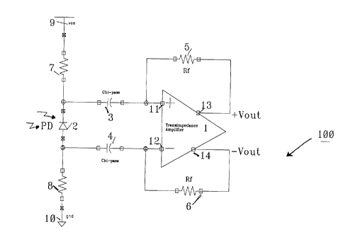
Fig. 1 is a schematic diagram of an integrated circuit infrared receiver using
a reverse biased
infrared photo diode, integrated high pass capacitors in a transimpedance
amplifier configuration;
Fig. 2 is a schematic diagram of the circuit of Fig. 1 illustrating associated
parasitic
capacitances;
Fig. 3 is a schematic diagram illustrating a bandwidth stabilized amplifier
circuit in
CA 02242724 1998-07-09
CA9-98-017 5
accordance with the invention.
Specific Embodiment of the Invention
In battery operated circuits, the battery voltage can vary by as much as 50%
during the course of
operation as the battery discharges. For integrated circuits, this can change
the internal dynamics of
their operation. For instance, in the circuit of Fig. 1, which illustrates a
sensitive low-noise
preamplifier circuit used for infrared signal detection, it is important that
a constant and controllable
bandwidth be maintained in order to ensure that the same signal to noise ratio
is maintained at all
supply voltages. Failure to do so, would result in a more limited operational
voltage range as
amplifier sensitivity would degrade outside the range.
Referring to Fig. I which illustrates an integrated circuit infrared receiver
100 using a reverse biased
infrared photo diode 2, integrated high pass capacitors 3, 4, and feedback
resistors 5, 6 in a
transimpedance differential amplifier configuration; it can be seen that the
integrated high-pass
capacitors 3, 4 are used in series with the inputs 1 l, 12 of amplifier 1 to
filter out ambient or low
frequency infrared noise.
The infrared photo diode 2 is used in a photo conductive mode by reverse
biasing it across supply
voltage Vee 9 and ground 10 using bias resistors 7, 8 as will be understood by
those familiar with
the art. When infrared light strikes photo diode 2 a photo current is
generated flowing from cathode
to anode, i.e. in the direction opposite to that of a diode used in the
conventional manner.
Referring to Fig. 2 which is based on diagram ofthe circuit ofFig. 1
illustrating associated parasitic
CA 02242724 1998-07-09
CA9-98-017 6
capacitances; it may be understood that the reverse biasing ofthe photo diode
2 generates a depletion
capacitance Cj 2p the value of which varies inversely with the supply voltage
Vee 9. In the
embodiment of the invention described supply voltage Vee is kept constant so
that there should be
no variation in its capacitance due to voltage variations.
Integrated high pass capacitors 3, 4 are formed using integrated circuit
technology on the substrate
used to form amplifier 1 for compactness and efficiency. In a typical high-
capacitance
implementation, the capacitor is constructed by placing a polysilicon layer
over an n-well region,
whereby the polysilicon layer forms the top plate of the desired capacitor and
the n-well forms the
1 o bottom plate of the desired capacitor. The n-well, however resides atop
the common p-type substrate
that is shared with the rest of the integrated amplifier circuit. As a result,
a parasitic capacitance from
the n-well back plate to the (grounded) substrate exists similar to that of
the deplection capacitance
formed in a reverse biased pn junction. This results in a parasitic
capacitance to ground that varies
inversely with the do voltage present on the back plate of the capacitor. This
is unlike the situation
with a discrete capacitor in which the amount of voltage used would not affect
the value of the
capacitor. In the case of the integrated capacitor described above, variations
in the parasitic
capacitance value of up to 25% have been observed with voltage variations of 2
V. The actual
variations are dependent on the integration technology used and the
capacitance structure chosen.
Regardless of the actual value of parasitic variation, variation in the front-
end capacitances of a low-
noise amplifier has detrimental effects on the overall performance.
We have found that in the case of a high pass integrated circuit capacitor,
the parasitic substrate
capacitance Csub can be fairly large (25 pF to substrate for a 500 pF
capacitor, for example) and that
the parasitic capacitance Csub varies to a first approximation linearly with
the supply voltage used
for bias. For example, a typical 500 pF polysilicon over n-well capacitor can
have Csub vary from
20 pF when the back-plate is at 2 Volts to 26 pF when the back-plate is at 1
Volt.
The parasitic capacitances Csub of high pass capacitors 3 and 4 are
represented by 3p and 4p
respectively in Fig. 2.
CA 02242724 1998-07-09
CA9-98-017 7
The effect of the parasitic capacitances of photo diode 2, capacitors 3, and 4
cause the following
effects: Parasitic capacitance 2p of photo diode 2 acts as a low pass filter
leaking high frequency
signal components from photo diode 2 to ground. The parasitic capacitances 3p,
4p respectively of
high pass capacitors 3, 4 respectively similarly leak high frequency signal
components from photo
diode 2 to ground. Although these effects can be taken into account when the
parasitics are invariant,
it becomes more of a problem when they are not. With integrated devices, the
parasitic capacitances
will grow with decreasing bias voltage thus decreasing the upper frequency
cutoff of the circuit and
thereby reducing its bandwidth. In effect, the bandwidth of the receiver
circuit illustrated in Fig. 1
is proportional to the supply voltage used for device biasing. We have found
this to be undesirable
l0 in infrared data communication as the performance of the device would vary
with its supply voltage.
The signal to noise ratio of a receiver such as the one illustrated is related
to bandwidth. It is
undesirable to have the signal to noise ratio vary with supply voltage as data
communication may
become unreliable in some circumstances. If the bandwidth is too large the
signal to noise ratio is
reduced as extra noise is admitted. If the bandwidth is too small the signal
level will be attenuated.
To illustrate the solution presented by the invention herein, some use will be
made of some well-
known electrical formulae.
The cutoff frequency, fc, of an RC circuit is given by the formula:
2o fc = I/(2* II R'~C) (Equation 1)
where conventional nomenclature is being used.
The input impedance of the amplifier portion of the circuit of Fig. 2
including the feedback loop
occupied by resistance Rf 5, RF 6 is given by the formula:
Rin = Rf/Ao (Equation 2)
CA 02242724 1998-07-09
CA9-98-017 8
where Rin is the input impedance, Rf is the value of the feedback resistance
Rf 5, and Ao is the
open-loop gain of amplifier 1.
For the circuit of Fig. 2, the input capacitance seen by the amplifier is:
Cin = Cj + (0.5*Csub) (Equation 3)
where Cj is the depletion capacitance of the photo-diode (2p) and Csub is the
parasitic capacitance
(3p,4p) of the high-pass capacitors (3,4) where the design value for the two
capacitors is the same.
The voltage dependence of Cin due to either Cj, Csub or the combination of
both may be further
1o expressed by rewriting the formula for Cin as:
Cin(V) = Cino*(1 +a(V)) (Equation 4)
where Cino is the initial value for Cin and the factor ( 1 +a(V)) denotes the
voltage dependent scaling
factor for Cino.
If the voltage dependence of Cin (i.e. Cin(V)) is substituted into equation l,
one gets
fc='/a II (Rf/Ao)*Cino(1+a(V)) (Equation 5)
2o where one can clearly observe the voltage dependence of the low-pass cut-
off frequency.
By now making the open-loop gain Ao a function of the voltage as well (as
described earlier), one
may represent the open-loop gain Ao as:
A(v) = Ao(1 +a(V)) (Equation 6)
If this relation is now substituted into equation 5 one reobtains the cutoff
frequency, fc, to be:
CA 02242724 1998-07-09
CA9-98-017
fc = 1/(2 II(Rf/(Ao( 1 +a(v))))*Cino( 1 +a(v)) (Equation 7)
which in turn becomes:
fc= 1/(2 II (Rf/Ao)* Cino (Equation 8)
The cutoff frequency, fc, has now become independent of voltage as illustrated
by equation 8. From
this it can be seen that the bandwidth of the amplifier and hence the signal-
to-noise ratio (SNR) can
to be kept constant over a wide voltage range, thereby ensuring proper
operation of the receiver. We
have found that the above conditions can be attained by designing the open
loop gain Ao of amplifier
1 to increase with decreasing supply voltage since the input capacitance, Cin,
increases with
decreasing supply voltage. Thus the effect of decreasing voltage in a battery
powered environment
can be remedied over a significant voltage range, e.g. from an initial 5 volts
to a final voltage of 2
1s volts.
The amplifier circuit of Fig. 3 depicts a differential amplifier 20 together
with its bias control
circuitry, current mirrors 40, 41.
20 Although the amplifier circuit depicted is somewhat simplified in nature,
it is suitable for
understanding, the nature and operation of the invention. The open loop gain
of amplifier 20 is
proportional to the collector bias current Ic in collector resistors 29, 30 so
that by controlling the
collector current we can control the open loop gain. By controlling the tail
current hail using
transistor 23, the collector current, Ic, can be controlled. The compensation
circuitry depicted in Fig.
25 3 is capable of controlling the collector current by sampling the supply
voltage Vdd (which may be
the battery voltage or proportional to it) and adjusting the collector current
Ic flowing through the
final amplifying transistors 24, 25.
Current mirror circuit 40 which includes diode connected transistor 20 biased
by the variable supply
CA 02242724 1998-07-09
CA9-98-017 l0
voltage 15 (produced by a power supply battery) is connected by its gate to
the gate of transistor 21.
'The current Isubm through transistor 21 mirrors the current Isub-ref (i.e. is
proportional to the
current) in transistor 20 so that any decrease in the supply voltage Vdd 15
will cause a reduction in
current Isubm. The second current mirror circuit 41 includes diode connected
transistor 22 and
transistor 23 the current through which mirrors the current through transistor
22. The reference
voltage Vee 9 for mirror circuit 41 is fixed in this embodiment so that the
current Iref is fixed and
the current through transistor 22, Irefin, becomes the difference Iref Isubm.
The current Irefm is
mirrored to the final amplifiers current source transistor 23 so that its
current, hail, is proportional
l0 to Irefm and can be represented by the formula, Iref(1 - b), where b varies
proportionally with the
supply voltage Vdd. It can be seen that when the supply voltage Vdd decreases
Iref will increase,
thereby increasing the open loop gain of the amplifier.
Therefore Ao is proportional to Itail which in turn is inversely proportional
to the supply voltage
Vdd. By setting the value of the bias resistors 27, 28 suitably, the gain of
the amplifier can be made
to compensate for changes in the effects of the parasitic capacitance of the
high pass capacitors as
the supply battery voltage decreases with use or time. As a result, the
bandwidth of the receiver
circuit can be held constant over a range of supply voltage.
Having described and illustrated the principles of the invention in a
preferred embodiment, it should
be apparent that the invention can be modified without departing from the
principles. Accordingly
I claim all modifications and variations coming within the scope of the claims
which follow.