Note: Descriptions are shown in the official language in which they were submitted.
' CA 02242743 1998-07-08
DIRECT CONVBItSION DIGITAL X-R~rY DETECTOR WITH INHERENT
HIGH VOLTAGE PROTECTION F'OR ~Tl~ITIC BIND DYNAIYIIC II~iAGING
BACKGROUND OF THE INVENTION
1. Field of the Invention
This invention relates to the acquisition of a
radiographic image using a large area, direct conversion,
solid state detector. More specifically, the present
invention concerns an electronic solid-state image
capture device for static and dynamic x-ray imaging
applications. In particular, it relates to devices using
a direct converter material, such as amorphous selenium,
a flat panel TFT array, and solid-state charge
amplifiers, such that the mode of operation prevents
excessive voltage built-up across the TFT array that
would be damaging to the TFT transistors.
2. Description of the Prior Art
A number of attempts have been made in the past to
minimize high voltage affect or to achieve high voltage
protection in image captur~ devices using a thin film
transistor (TFT) array.
For example, in the paper by Zhao Wei, Law James,
Waechter D., Huang, Z., and Rowlands J., entitled
"Digital Radiology using active matrix readout of
amorphous selenium detectors with high voltage
protection", 1998, Med Phys 25 (4), pp. 539-549, a
selenium-based x-ray imager with a special TFT dual-gate
structure is disclosed which provides a high voltage
protection. The dual gate structure provides the high
-1-
' CA 02242743 1998-07-08
voltage protection by forming a back channel in the TFT
structure if the pixel voltage exceeds a certain
potential, thus discharging the storage capacitor. Its
main drawback comes from the fact that the saturation
potential is controlled by deposition factors in the
processing of the TFT array (i.e. ratio of oxide
thickness of top and bottom gate insulators), and
therefore cannot be externally controlled. The polarity
of the bias voltage for the selenium layer in this
1o example is positive high voltage.
In PCT International Application WO 96/22616
published July 25, 1996, a TFT structure is described
which minimizes the charge injection of the TFT switching
for x-ray detectors. In this case, no mention is made
about the high voltage protection, and the polarity used
to bias the selenium layer is positive high voltage.
In U.S. Patent No. 5,198,673 of March 30, 1993 by
Rougeot et al., a photosensitive selenium-based x-ray
imager is described where the high voltage protection is
provided by the presence of a second two-terminal
protection device resident at each pixel location. This
technique suffers from the fact that array construction
is more complex, and that array yields may suffer as the
pixel size is decreased since more and more circuitry
must be placed on a smaller pixel size. Also, the
saturation voltage of the pixel is determined by TFT
array processing conditions, and therefore cannot be
externally controlled.
-2-
i
CA 02242743 2002-05-30
In a paper by Lee D., Cheung L.K., and Jeromin L.,
entitled "A new digital detector for projection
radiography", 1995, SPIE Vol. 2432, pp. 237-249,
selenium-based TFT imaging system is disclosed where a
thick dielectric layer is interposed between the high
voltage bias electrode and the selenium layer. Thus, the
high voltage protection mechanism comes from the fact
that negative charges accumulate at the interface between
the selenium layer and the insulator layer, thereby
lowering the electric field and x-ray sensitivity of the
selenium layer. However, this technique suffers from the
fact that the negative charges must be eliminated prior
to making a successive image, and hence this technique
cannot be used for real-time imaging applications.
In U.S. Patent No. 5,598,004 of Jan. 28, 1997 by
Powell et al. and U.S. Patent No. 5,396,072 of March 7,
1995 by Schiebel et al. photoconductor-based imaging
detectors are described, where one of the embodiments
uses a selenium-based energy conversion layer. However,
no mention is made of the high voltage protection of the
TFT array.
In U.S. Patent No. 5,528,043 of June 18, 1996 by
Spivey et al., a selenium-based system is described,
where the active substrate uses a metal oxide
semiconductor (MOS) circuit technology on silicon wafers,
rather than TFT technology on glass substrates. In this
technology, the design rules allow for a higher degree of
integration, and therefore do allow to incorporate
-3-
' CA 02242743 1998-07-08
several transistors per pixel. This allows, for example,
the use of a buffer to non-destructively read out a
pixel, but does not mention wh~ther high voltage
protection of the circuit from the selenium bias is
achieved.
In U.S. Patent No. 5,436,101 of July 25, 1995 by
Fender et al., there is described a selenium structure
which can be charged negatively by placing a blocking
layer between the selenium and the substrate, but there
is no mention of any high voltage protection of any
element on the substrate.
Finally, in Canadian Patent Application No.
2,184,667 by Alain Jean and Bradley Trent Polischuk,
published on March 4, 1998, and corresponding European
Application EP 0 826 983 also published on March 4, 1998,
a selenium multilayer structure is disclosed which, in
addition to providing for real-time imaging capabilities,
also leads to increased mechanical durability. However,
no indication of how this structure could be used for
high voltage protection is given.
OBJECTS AND SUMMARY OF THE INVENTION
It is an object of the present invention to overcome
the various defects and limitations mentioned above by
allowing a direct external control of the built-in
voltage on the pixel capacitor.
A further object of the present invention is to
achieve the desired high voltage protection by providing
a photoconductor layer that can be biased negatively.
-4-
' CA 02242743 1998-07-08
A still further object of the present invention is
to fabricate a stack of layer forming a selenium p-i-n
structure which allows negative bias at a very low dark
current.
Other objects and advantages of the present
invention will become apparent from the following
description thereof.
In essence, the present invention comprises a direct
conversion x-ray image electronic detector which has an
n-channel active matrix thin film transistor (TFT)
substrate, a coplanar selenium diode structure and a high
voltage biasing electrode and in which high voltage
protection is achieved by setting the high voltage
biasing electrode to a negative potential and the TFT
"off" gate voltage to a predetermined negative value,
such that the TFT is essentially non-conductive. Such
voltage is typically in the range of -1V and -20V and
preferably about -lOV. In this regard, there will always
be some TFT leakage, however the negative "off" gate
voltage may be adjusted so as to minimize the same and
render the TFT essentially non-conductive.
The saturation exposure of the x-ray image
electronic detector can be adjusted by changing the
negative value given to the "off" gate voltage. Also, an
external gain control may be obtained by changing the
value of the negative high voltage on the biasing
electrode which is typically between 1kV and 3okV.
The detector should also be provided with suitable
-5-
CA 02242743 1998-07-08
charge amplifiers such as to sink the current coming from
the TFT arrays.
In a preferred embodiment, the novel x-ray
electronic detector uses a selenium p-i-n multilayer
converter layer as a signal current source to avoid time
delays in emptying and replenishing material charge
traps. As is know, the p-i-n structure is a diode with
the i layer sandwiched between the p and n layers.
BRIEF DESCRIPTION OF THE DRAWINGS
A preferred embodiment of the present invention will
now be described with reference to the appended drawings
in which:
Fig. 1 is a perspective view of a structure of a
detector in accordance with this invention;
Fig. 2 diagrammatically illustrates a portion of a
two dimensional TFT matrix where each pixel element
contains a storage capacitor and a TFT transistor;
Fig. 3 represents a cross-section of the energy
conversion layer, composed of three such layers
designated as p-type, i-type and n-type, thus p-i-n;
Fig. 4 shows a measured current versus electric
field characteristic for a photoconductor structure which
contains a p-i-n device.
Fig. 5 shows the current flow through the channel of
the TFT at various pixel voltages for a gate voltage of
-lOV, and the insert in this figure shows a measured
drain current as a function of applied gate voltage;
-6-
CA 02242743 1998-07-08
Fig. 6a and Fig. 6b are schematic representations of
a single pixel collection electrode, a storage capacitor,
TFT, integrating amplifier and selenium p-i-n structure
in Image Acquisition Mode and Image Saturation Mode
respectively; and
Fig. 7 is a graph of a measured pixel response as a
function of input signal charge for gate off potentials
of -5 V and -10 V.
DETAILED DESCRIPTION OF THE INVENTION
In the Figures, the same elements are identified by
the same reference numbers.
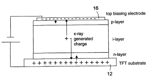
Fig. 1 illustrates a preferred embodiment of the
novel large area direct conversion digital solid state
detector 10 for the acquisition of a radiographic image.
It is comprised of an active matrix thin film transistor
(TFT) substrate 12, a co-planar p-i-n selenium diode
structure 14 and a high voltage (HV) biasing electrode
16. The TFT active matrix is further comprised of a two
dimensional array of pixels 18 each of which can be
individually addressed by the corresponding data and gate
lines. Integrated into each pixel 18 is a collection
electrode 20, a charge storage capacitor 22 (see Fig. 2),
and a TFT metal-oxide-semiconductor-field effect
transistor 24 (MOSFET) which serves as a switching device
to gate the charg~ from the storage capacitor to the
amplifier 26 located at the termination of the data line
(see Fig. 2). The selenium p-i-n structure 14, whose
CA 02242743 1998-07-08
function will be described later, is deposited directly
on to the TFT active matrix 12. Finally, a large area
conductive metal electrode 16 is deposited on top of the
p-i-n structure 14 to serve as the high voltage biasing
electrode 16 for the detector 10.
This detector 10 can be used to acquire an x-ray
image as follows: The selenium p-i-n structure 14 has
been designed and optimized such that it has a very high
transversal resistance in the dark, as well as very high
lateral r~sistance (see Fig. 4). Under dark conditions,
the current that flows through the p-i-n diode is
extremely small (-20pA/cmZ) even when large bias voltages
are applied to the device. Wh~n an x-ray photon impinges
the detector 10, the photon is absorbed in the bulk of
the selenium structure 14, and electron hole pairs are
generated in the volume of eel~nium at the location where
the x-ray photon was absorbed. The high voltage bias on
the structure serves two purposes - first, it enhances
the sensitivity of the seleniua by preventing geminate
recombination, and it also enables the carriers to reach
their respective collection electrodes without trapping.
The drift of these carriers in the selenium p-i-n
structure 14 causes a displacement current to flow in the
storage capacitor 22 immediately underneath the location
of the selenium where the x-ray photon was absorbed.
Consequently, in the absence of any leakage path, the
voltage across the storage capacitor 22 at that
particular location increases linearly proportionally to
-g-
CA 02242743 1998-07-08
the current flowing into it. The final voltage that is
attained on the storage capacitor 22 after the x-rays
have terminated is thus proportional to the number of x-
ray photons that were absorbed in the volume of selenium
immediately above each collection electrode. Each storage
capacitor 22 will attain a different final voltage,
corresponding to the spatial representation of the x-ray
fluence striking the detector 10 and hence represents the
radiographic image of the patient.
Fig. 2 further illustrates the two dimensional TFT
active matrix 12 where each pixel element 18 contains a
storage capacitor 22 and a TFT transistor 24, and the
entire array is coated with a continuous selenium p-i-n
structure 14 (which is represented in Fig. 2 as a current
source in parallel with a selenium capacitance at each
pixel location). Also shown in Fig. 2 are gate drivers 25
and read out amplifiers 26, which are either integrated
directly onto the glass substrate, or attached to the
glass by wire bonding, or other interconnect technology
such as chip-on-glass, and the like. The image is read
from the detector by turning on the TFT transistors 24 at
each pixel location 18 in a multiplexed fashion by
sequentially activating each gate line with the gate
drivers 25 and allowing the charges on each storage
electrode to flow through the pixel TFT channel, and
along the data lines to a charge sensitive amplifier 26
located at the termination of each data line. The
function of the charge amplifier 26 is to integrate the
-9-
CA 02242743 1998-07-08
charge, and output a low noise buffered signal that is
proportional to the amount of charge integrated during
the readout. Each charge amplifier voltage is sampled by
an analogue to digital (A/D) converter (not shown), and
the corresponding digital values are stored in memory of
a host computer (not shown) for subsequent image
reconstruction, analysis, and display. Each charge
amplifier 26 may be provided with an input protection
device 28 to protect the charge amplifier 26 in
exceptional circumstances when it may become overloaded.
As previously mentioned, the high voltage is
required for making the selenium sensitive to x-rays, and
this voltage is such as to produce electric fields
between about 2V/~m and 70V/~cm in the selenium structure.
As already mentioned previously, this voltage is
typically between 1kV and 30kV. If the leakage of the
selenium structure is too great, or if a large x-ray
exposure substantially lowers the resistivity of the pi-
n structure 14, then an appreciable fraction of this high
voltage bias will fall across the integrated storage
capacitor 22 on each pixel element. Catastrophic
breakdown of the dielectric in the storage capacitor 22,
for example SiOz or SiN, may result if the voltage gets
too high. Further, since the source of the TFT MOSFET 24
is also connected to the storage capacitor 22, (see Fig.
6a), a substantial voltage may develop between the source
and drain of the MOSFET leading either to punch through
in the gate dielectric or damage to the channel of the
-10-
CA 02242743 1998-07-08
device itself. It is therefore extremely important to
prevent the pixel voltage from building up beyond the
critical voltage level to avoid damage to the array if it
is subjected to a fault condition, such as a large x-ray
over-exposure.
Thus, the present invention, relating to the
protection of the TFT 12 from high voltage damage, uses
two separate enabling elements in combination with one
another - namely a suitably designed low dark current,
negative-biased photoconductor structure for direct x-ray
conversion, and a suitably designed n-channel TFT active
matrix for charge storage and readout. The photoconductor
converter may consist of CdTe, PbO, HgI2, CdSe, or similar
materials. In the preferred embodiment of the present
invention, the x-ray converting photoconductive structure
is composed of doped amorphous selenium.
Fig. 3 represents a cross section of the energy
conversion layer, where it is indicated that there are
essentially three such layers designated as p-type, i-
type and n-type. The n-type and p-type layers function as
one way charge valves, or blocking layers, to block the
injection of charges from their respective electrodes
into the selenium i-layer. The top blocking layer, called
the p-layer, is named so b~cause it is selectively doped
so as to degrade the transport of electrons through it,
while leaving the hole transport relatively unaffected.
In this context, the layer is called p-type because any
photoconductive drift current through this layer is
-11-
CA 02242743 1998-07-08
composed only from the drift of holes. The bottom
blocking layer, called the n-layer, is named so because
it is selectively doped to dsgrade the transport of holes
across its thicknea, leaving the transport of electrons
relatively unchanged. In this context, this layer is
called n-type because any photoconductive signal through
this layer is due to drift of ~lectrons only. The middle
layer in the structure, called the i-layer, is a doped
amorphous selenium alloy which has been optimized in
terms of maximizing both the electron and hole transport
through the thickness of the i-layer. By sandwiching the
appropriate blocking layer between the i-layer and the
respective electrode, it is thus possible to
substantially reduce the dark currents which flow through
the photoconductor material, since the major contribution
to the total dark current in these high resistive
materials is charge injection from the electrode
materials.
Fig. 4 is a measured currant versus voltage
characteristic for a photoconductor structure which
contains the n and p blocking layers (called the p-i-n
device). In this and other figures, reference to "E"
means "exponential". Thus 1E-6 means 10-6 and so on. The
thick i-layer of the p-i-n device is composed herein of
doped amorphous selenium that is 500~cm thick. The top
electrode material in this case is Pd, although other
technologically suitable materials such as Au, A1, Mo and
Pt may be used. The bottom electrode material in this
-12-
CA 02242743 1998-07-08
case is indium tin oxide (ITO) on glass, suitably chosen
because of its widespread use in the LCD manufacturing
process for the TFT active matrix arrays, although other
materials such as A1 may also be used. The measured
current in Fig. 4 is almost 1000 times lower than the
current which flows in a Schottky device that is biased
under similar conditions. Schottky devices are known in
the art. When such Schottky devices are biased
negatively, the dark current which flows therein is
prohibitively large, around l~cA/cm2 at a bias voltage of
-5000V, to be used in this bias condition for an x-ray
detector. In sharp contrast to this, the p-i-n device of
the present invention biased under similar conditions has
a dark current more than five orders of magnitude lower,
and in this case around 20pA/cmZ which is more than
adequate for practical use in an x-ray detector.
The second enabling element of this invention is an
n-channel TFT array, the typical characteristics of which
are illustrated in Fig. 5. Typically, the TFT structure
is formed by depositing a metal, which serves both as the
gate of the TFT and one electrode of the storage
capacitor, onto a glass substrate. To form the gate oxide
and the dielectric of the storage capacitor, a thin layer
of dielectric, for example SiN or Si02 is deposited.
Following the dielectric material deposition and
patterning, the semiconductor material, typically a-Si:H,
p-Si or CdSe, is deposited onto the structure to serve as
the channel of the TFT. To facilitate ohmic contacts to
-13-
CA 02242743 1998-07-08
contact regions may be sel~ctively doped n' to lower any
internal potential barrier. Source and drain metals are
then deposited onto the structure to make electrical
contact to the TFT. A thick passivation layer, typically
several microns thick, is then deposited onto the
structure prior to the deposition of the pixel electrode
metal. This metal electrod~ makes contact to both the p-
layer of the selenium coplanar p-i-n diode as well as the
integrated storage capacitor. The pixel electrode
material may extend over the top of the active TFT to
improve the fill factor of the device. The inset of Fig.
5 shows a measured drain current Id as a function of
applied gate voltage for a typical a-Si:H TFT. Although
the a-Si:H is a law mobility material, a reasonable
device on current of about 1~A and a very low off current
<10-1~ A can be achieved by controlling the geometry of
the transistor. If the TFT gate is held at a constant
voltage of -lOV, which is typically used to turn the TFT
into their off state, and the pixel voltage is allowed to
float negatively, it can b~ seen from Fig. 5 that the
current Id which flows through the channel of the TFT
remains relatively low for pixel voltages up to about
T7V. In other words, the TFT remains in its high
impedance state. However, as the pixel voltage decreases
beyond -7V, the current through the channel of the TFT
starts to increase dramatically, despite the fact that
the TFT gate voltage is still maintained at its off
-14-
CA 02242743 1998-07-08
potential.
Fig. 6a and 6b schematically show a single pixel
collection electrode 20, a storage capacitor 22, TFT
MOSFET 24, integrating amplifier 26, and selenium p-i-n
structure. During a normal image acquisition process
shown in Fig. 6a, the voltage on the gate of the TFT is
typically around -10V, which places the TFT in its off
state (drain to source resistance around 10150 and forces
all of the current generat~d in the selenium p-i-n layer
by the x-rays to charge up the storage capacitor 22. This
causes the floating node 29 to go from around zero volts
to a negative voltage which, in this example, is
indicated to be around -2V. After the x-rays have elapsed
(static imaging) or at a repetitive frame rate (dynamic
imaging), the gate voltage is turned from -lOV to its
"on" voltage, typically around +20 volts, to place the
TFT in its "on" state (drain to source resistance around
1060 . This allows the charge to flow from the storage
capacitor through the TFT channel, to the charge
integrating amplifier 26, thus providing a signal to be
sampled by the A/D. It should be noted that this image
readout process also resets the signal voltage on the
storage capacitor to a preset reference voltage, such as
zero volts, to allow for another image to be acquired.
If, however, during the image acquisition phase the
current through the p-i-n structure is too high, then the
voltage on the storage capacitor 22 would build up to a
larger value, as indicated in Figure 6(b). In the absence
-15-
CA 02242743 1998-07-08
of any protection mechanism, the storage capacitor
voltage can build up until device failure occurs, thus
limiting the usefulness of the imaging detector for
extreme imaging applications. This excessive current
could be due to high x-ray overexposure, for example, or
an electrical defect in the selenium layer. In this
particular case, however, once the voltage on the
capacitor exceeded -lOV, then the gate-to-source voltage
on the n-channel TFT MOSFET would become positive, thus
lowering the channel resistance of the TFT. In other
words, the TFT would turn on despite the fact that the
gate voltage was still in its off state (i.e. -lOV). The
excess saturation charge then will flow through the TFT
where it either gets neutralized by current flowing in
the amplifier, or in extreme cases, dissipates to ground
through specially designed input protection device 28 on
the amplifier 26 to prevent damage to that particular
channel of the amplifier 26. A simple reset sequence of
the amplifiers by reset 30 prior to initiating the read
sequence for the entire panel is required to flush the
excess charges which accumulated on the feedback
capacitance of the amplifiers on the lines where certain
pixels saturated. This eff~ct can be used to prevent the
pixel storage capacitor on the TFT from building up to a
damaging potential voltage during excessively large x-ray
exposures.
Fig. 7 shows a measured pixel response as a function
of input signal charge for gate off potentials of -5 V
-16-
CA 02242743 1998-07-08
and -10 V. It can be seen that in either case, the pixel
voltage increases linearly with increased signal charge
for low levels. However, as the signal charge exceeds
7.5 pC and 15 pC (1 pico-Coulomb), the pixel voltages
begin to saturate respectively at a value of about -5 V
and -10 V, which is far lower than the critical voltage
required to damage the TFT array. Moreover, increasing
negative gate off voltages allows the pixel voltage to
build up to higher potentials, thus increasing the
dynamic range of the system. Therefore, the saturation
voltage can be externally modified by adjusting the gate
off voltage, which is significantly simpler than altering
process steps during the fabrication of the TFT array as
disclosed in some prior art references.
It should be understood that the invention is not
limited to the specific embodiments described above, but
that modifications obvious to those skilled in the art
are also included therein. For example, reference to
x-rays also includes gamma rays which are similarly used
in medical and other applications. Also, in lieu of p-i-n
diodes, which have been described herein by way of a
preferred example, other photoconductors can be used
within the scope of the present invention, such as TlBr,
PbI2, PbO, HgI2, CdTe, CdZnTe and the like.
-17-