Note: Descriptions are shown in the official language in which they were submitted.
CA 02242920 1998-07-10
W O 97/25688 PCT/GB97/00053
"Improvements in or relating to sm~rt cards"
THIS INV~NTION relates to a system for smart cards. The
invention relates to a pouch sys~em for smart cards and, in
particular, non-contact smart cards, to contact and non-
contact smart cards adapted for use with the pouch system,
and to the provision of a system employing a plurality of
such pouches and such cards.
Smart cards contain a surface mounted or embedded
chip on the card. This chip contains a microprocessor and
a memory area. The data stored in the memory area is
accessible when the card is inserted into an appropriate
form of card reader. Some of the memory area is usable
during the course of the transaction to record new data
received by the card from the card reader. Such a smart
card has an array of contact pads, generally o~ gold, which
are positioned in a standard arrangement on the card face.
The power supply to the card is provided through the
contact pads.
To conduct a card transaction the smart card is
inserted into an appropriate card reader, which makes
electrical contact with the contact pads. The chip
microprocessor is then powered up and, following an
appropriate handshake, a transaction is conducted according
to parameters entered at the reader side.
It is desirable to use smart card technology in
environments where it would not be appropriate or
convenient physically to insert a card into a card reader.
Such circumstances are, for~ example, in mass Itr~-.sit
systems, in road tolling, in car park ticketing and for
automated warehouse control. Accordingly, non-contact
CA 02242920 1998-07-10
W O 97/25688 PC T/G B97/00053
smart cards have been developed. Such cards are similar to
the cards described above (referred to below as contact
cards), but instead of transmitting and receiving data
through metal contact pads on the card surface, data is
received and transmitted by means of an antenna loop and an
induction coil to emit and receive electromagnetic waves at
an appropriate frequency.
Such cards can be powered in different ways. In
one form of card, a small battery can be mounted on the
card to power the chip which can be kept in a "sleep mode"
at times when no transaction is to be conducted and brought
to full operation when a signal from an appropriate signal
source is detected. In another form of card, there is no
power source on the card itself and power is provided from
outside by inducing a current in an induction coil mounted
in the card. When the card is brought into proximity with
a larger external coil with significant current flowing
through it, current is induced in the induction coil in the
card by means of inductive coupling. This current powers
the chip on the card which then boots up, handshakes and
conducts the desired transaction. An advantage of this
system is that unauthorised access to the card is
relatively difficult as, in addition to the necessary
signals for communication with the card, the card must also
be sufficiently close to an appropriate external coil for
it to be powered up. In known systems, this distance is
typically in the region of 10 cm.
A difficulty with the existing non-contact cards is
that their range ~r operation is relatively small as it is
not practical co place a large ~ ~ a ~--na aL-rangement
in or on a s.nart card naving an I~-defined stclndard size.
The antennae used -ire essentia'ly of normal wire ~ut with
a high ca-bon concent and are often sha~d (particl-lar~,y by
CA 02242920 1998-07-10
W O 97/25688 PCT/GB97/00053
use of wire of a D-shaped cross-section) to enhance their
effectiveness and to give them directional properties.
Even after optimisation of the antennae, a reading
range of 15 cm or so is typical. There also still exists
the problem of unauthorised access to the card. Although
it is difficult to achieve such access because of the close
proximity to a card reader required to effect
communication, it is nonetheless not impossible. It is
moreover possible that use of more powerful transmitters
could enable access to the card at greater distances.
Accordingly, the present invention provides a pouch
system for smart cards, wherein said pouch system is
provided with electrical contacts for connection with
electrical contacts of an inserted smart card, thereby
changing in use the capacity of the inserted card to
receive and/or transmit external signals.
Further, this invention provides a smart card for
use with a pouch system, which smart card comprises semi-
conductor circuitry including a memory section and further
comprises an induction coil and an antenna, said semi-
conductor circuitry by conducting tracks, said semi-
conductor circuitry being connected to contact pads formed
on the surface of the card.
So that the invention may be more readily
understood, embodiments thereof will now be described, by
way of example, with reference to the accompanying
drawings, in which:
Figure 1 is=a plan view of a~ smart card ~mbodying
the present invention shown with the top lamin~te laye~s
CA 02242920 1998-07-10
W O 97/25688 PCT/GB97/00053
removed to expose a chip, antenna and induction coil
mounted on an intermediate layer in the card;
Figure 2 is a plan view of a top surface of the
card of Figure l; and
Figure 3 is a schematic view of one half of a pouch
embodying the present invention for receiving the card of
Figures 1 and 2, the plan view of the other half
corresponding.
Conventional smart cards comprise a number of
laminated layers, A chip is typically located on the card
after some, but not all, of the lamination layers have been
formed. Smart cards embodying the present invention, such
as that shown in Figures 1 and 2, need not have the chip
embedded at an intermediate stage of the lamination
process, It is possible to form a card by lamination and
then to mount the chip on top of the card, A typical card
is in the region of 30 thousandths of an inch thick
(0.76mm).
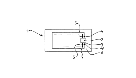
Figure 1 shows a card 1 embodying the present
invention from which the top lamination layers have been
removed to expose a chip 2, Tracks 3 on the card 1 are
laid down to lead from the relevant pin connections 4,41,
5,5' of the chip 2 to an antenna loop 6 and an induction
coil 7. The antenna loop 6 and the induction coil 7 are
shown schematically in Figure 1,
Referring to Figur~ ~, two pairs of contact pads
8,8', 9,9' are formed c-.l each side 10,~ ~f ~ht ' ~A 1.
Contact pads 9,9' c~nnot be see~ in Figure 2 as t~ey are c,n
the opposite side 11 of the ,-ard 1. Preferaoly, contact
pads 8,8', 9,9' are ~ormed on the card 1 by the ar,~licatLcn
CA 02242920 1998-0i-10
W097/25688 PCT/GB97/00~3
~ of a conductive paint. In Figure 2, the contact pads 8,8',
9,9' are shown as two adjacent parallel rectangular blocks.
The contact pads 8,8', 9,9' may be in the form of text or
symbols or formed as part of a design on the card 1.
Electrical connection is made between a respective
contact pad 8,8', 9,9' and a respective pin connection
4,4', 5,5' of the chip 2 by pinning through the card
laminate. Thus, contact pad 8 is electrically connected to
pin connection 4, contact pad 8' to pin connection 4' and
contact pads 9,9' are respectively electrically connected
to pin connections 5,5'.
In a preferred embodiment, a solid or hollow brass
pin (not shown) having a length slightly greater than the
thickness of the card 1 is punched through the card 1 so
that it passes through and ohmically contacts a respective
pin connection 4,4', 5,5'. An end of each pin protrudes on
either side of the card 1. The protruding ends of the pin
are flattened to form lands for facilitating electrical
contact with the pins and, hence, the respective pin
connections 4,4', 5,5 t . The contact pads 8,8', 9,9' are
formed on, or connected to, the flattened pin lands. For
a card 1 of typical thickness, 30/l,OOOths of an inch thick
(0.76mm), a pin which is some 6/l,OOOths of an inch
(0.15mm) longer is used.
The contact pads 8,8', 9,9' provide an enlarged
area of electrical contact to the chip 2. The contact pads
8,8', 9,9' comprise the contact connections to the antenna
loop 6 and the induction coil-7 within the card 1 and form
~ne~ 7~ -7tnL~ which the chip 2 can be powered up and
another path 6 through which the card 1 can transmit and
recei~re signals.
CA 02242920 l998-07-l0
Wo 97/25688 PCT/GB97/00053
The contact pads 8,8', 9,9' on the card 1 enable
co-operation with a pouch system embodying the present
invention. One side of a pouch 12 embodying the invention r
for use with the card 1 of Figures 1 and 2 is shown in
Figure 3. The other side of the pouch comprises a mirror
image of the first side. When sandwiched together, the two
sides form a slot 12A in which a card 1 may be inserted.
A pouch 12 in the pouch system retains a card 1 in the same
manner as pouches in conventional credit card wallets.
However, the pouches 12 of the pouch system are also
provided with electrical contacts 13,13l, 14,14' within the
slot 12A for connection with the contact pads 8,8', 9,9' of
a smart card 1 retained in the pouch 12 to change the
capacity of the smart card 1 to receive and transmit
external signals.
Pouches 12 in the pouch system may have different
configurations. In one configuration (not shown) of pouch
12, electrical contacts formed on the pouch 12 are
electrically connected to one another to short together the
two contact pads 8,8', 9,9' on the card 1 which link the
respective inputs on the chip 2 for powering up the chip 2
through the induction coil 7. This has the effect that
when the card 1 is inserted in the pouch 12, it is ~uite
impossible ~or the card 1 to be involved in any transaction
because it is not possible to provide power to the card 1.
This configuration of pouch 12 enables the card 1 to be
placed in a so--called "park" position in which the card 1
is stored securely in the pouch 12 without there being any
danger of unauthorised remote access.
The pouch system may also comprise other }~ouch
configurations in which the connection between ele~ rical
contacts 13,13~, 14,14' on the pouch 12 ~re~er~ ing to
Figure 3) and the electrical contacts 8,8', 9,9 on the
CA 02242920 1998-07-10
W O9~/25688 PCT/GB97/0~0~3
~ card 1 is used to different effect. In a second
configuration, which may involve no more than re-
orientation of the card 1 within a single pouch 12, or may
alternatively involve placing the card 1 in a separate
pouch 12' (not shown), the contact pads 8,8', 9,9'
associated with the antenna loop 6 and the induction coil
7 contacts are connected to another and much larger,
antenna loop 15 and induction coil 16 combination
associated with the pouch system itself. This enables the
card 1 to be read at a greater distance than would be
possible for a conventional non-contact smart card using
only the antennae within the card.
A particularly useful embodiment of this
configuration (not shown) involves the placement of a card
1 in a pouch 12 which is fixed to the windscreen of a car.
An antenna loop and induction coil combination formed of
appropriate conducting paint or in another appropriate
manner is fixed on the surface of the car windscreen and
forms the power and signal pick-up for the smart card.
This embodiment is especially suitable for mass transit
applications such as road tolling as it thus becomes
possible to take a toll from a car carrying a smart card
without any need for unduly close proximity between the
card and the card reader.
In a further configuration (not shown) of the pouch
system, either an additional pouch, or an additional
orientation within the same pouch 12, is provided in which
there are no electrical connections between the pouch 12
and the card 1 retained within it. In these circumstances,
'- the non--cont~,L -m~i~ ca~ ill operate in the same manner
as a conventional no~-_ontact ~mart card having a range in
the region of 10 cm - i.e. a configuration in which the
range is not extended and the carrl 1 is not disabled.
CA 02242920 1998-07-10
W O 97/25688 PCT/GB97/00053
Another useful embodiment for the non-contact smart
card comprises use of the smart card as an intelligent
luggage tag, the luggage tag itself comprising a pouch
system embodying the present invention. Luggage tagged in
this manner may be tracked whilst out of contact with the
luggage owner. Rather than using the smart card itself, it
is envisaged that the smart card may be cloned to provide
card clones having either the same or a limited version of
the information contained on the master smart card for use
as such intelligent luggage tags.
It is envisaged that standard ISo cards may be
adapted for use as non-contact smart cards embodying the
present invention.
Methods of forming smart cards by embedding a chip
within a laminated card are well known and are not
discussed. Also known, is the provision of a non-contact
smart card with an antenna loop and an induction coil
formed on it. Non-contact smart cards in accordance with
this invention can be produced using appropriate techniques
and materials known for existing non-contact smart cards.
The previously described technique of making
electrical and mechanical contact with the various elements
within the card laminate using a through pin (not shown)
may be modified to improve such connections either within
or between laminates. The through pin is provided with
pre-selected regions along its length which, under
compression, increase in diameter or form, for example,
fingers in a star pattern which radiate outwardly from the
~in to make good electrical and mechanical contact with the
r_spective element in or between laminates. In this manner
a lan~ is ~ormed within the card. The pre-selected regions
in the pin are selected to correspond to the position
CA 02242920 1998-07-10
W O 97/25688 PCT/GB97/0~053
~ within the laminate at which the element to be contacted is
located. The terminations of the element to be contacted
by the land may be, for example, circular holes for
receiving a through pin or in the shape of a star cut-out
to accept the radiating fingers from the pin.
The means of exchange of data between non-contact
smart cards as employed in the invention and card readers
can be as for existing non-contact smart cards. The
software stored within the chip can be in accordance with
existing non-contact smart cards systems and information
exchanged can be according to known protocol. The card
readers employed to conduct transactions with the cards and
to power the cards may again be as are employed in existing
non-contact smart card systems.
A contact smart card having semi-conductor
circuitry but no internal induction coil and antenna can be
used with the pouch system of the present invention by
providing electrical connection between the semi-conductor
circuitry and contact pads formed on the surface of the
card. Such connection would allow the card to use the
induction coil and antenna of the pouch system thereby
allowing the card to operate as a non-contact smart card.
.