Note: Descriptions are shown in the official language in which they were submitted.
CA 02243133 1998-07-10
- 1 -
S/N MEASURING CIRCUIT AND MgTHOD, TRANSMITTING ELgCTRIC
POWgR CONTROL APPARATUS AND DIGITAL COMMUNICATING SYSTEM
BACKGROUND OF THE INVENTION
The present invention relates to a transmitting electric
power control apparatus used in a digital mobile
communicating system.
In a digital mobile communicating system, transmitting
electric power control is used for suppressing consumption
of electric power at a mobile station while maintaining
reception quality at a desired value, and for avoiding
unnecessary interference with other mobile stations.
Especially, in a CDMA (Code Division Multiple Access)
system, due to the existence of common frequency
interference (interference with other users) inherent in a
multiple system, the transmitting electric power control
is essential. In the CDMA system, generally, closed-loop
type transmitting electric power control is used, in which
a Signal-to-Noise Power Ratio (referred to as an S/N,
hereinafter) is measured from a signal received and
demodulated at a base station, instruction is sent to the
mobile station so that this S/N value will be a value
enough for desired reception quality, and transmitting
electric power is sequentially controlled. A noise N used
here includes a thermal noise and an interference signal.
CA 02243133 2002-10-17
. 74790-25
- 2 -
In order to conduct transmitting electric power control
with good accuracy, it is necessary to correctly measure
the S/N in a receiving device.
Fig. 4 is a view showing an S/N measuring
circuit of a first prior art. As shown in Fig. 4, an S/N
measuring circuit 50 of the first prior art is constructed
of a modulation removing circuit 3 connected to an analog-
digital (A/D) converter 2, a first averaging circuit 4, a
first square operating circuit 5, a second square
operating circuit 6 connected to the analog-digital (A/D)
converter 2, a second averaging circuit 7, a subtracting
circuit 8, and a dividing circuit 9.
In this first prior art, first, a demodulated reception
signal is sampled at a modulation clock by the A/D
converter 2. In the S/N measuring circuit, after a
modulated component of an output of the A/D converter 2 is
removed in the modulation removing circuit 3, the output
is averaged over a plurality of symbol sections in the
first averaging circuit 4, and an amplitude value in which
a noise component is suppressed is obtained. An output of
the'first averaging circuit 4 is squared by the first
square operating circuit 5, and desired signal Bower S is
obtained.
CA 02243133 1998-07-10
- 3 -
On the other hand, an output of the A/D converter 2 is
supplied to the second square operating circuit 6, and is
converted into time series having a dimension of electric
power. Thereafter, the output is averaged over a plurality
of symbol sections by the second averaging circuit 7, and
total electric power P of demodulated signals is obtained.
The subtracting circuit 8 obtains noise electric power N
by subtracting the desired signal power S from the total
electric power P of the demodulated signals. The dividing
circuit 9 receives the obtained S and N as above, and
calculates a ratio S/N thereof.
If representing the above-mentioned operation by an
equation, it is represented as an equation (1) below. A
series of sampled values of demodulated signals are
assumed as rk (k = 1, 2, "', M, M is a positive integer.).
If an amplitude of a signal point in which a noise is
suppressed is A, the desired signal power S is shown by
two equations described below.
A = ~ ~ rk r k (1) (r x is a decision symbol.)
S = ~ A ~ 2 (2)
Hereupon, a noise component superimposed over a
demodulated signal shows a Gaussian distribution of which
center is at the amplitude A of the signal point in the
absence of the noise, and the noise electric power N is
CA 02243133 1998-07-10
- 4 -
given by the following equation (3):
N - M ~ ~rk r k _ A) z ~3)
The above-described equation (3) can be transformed into
the following equations (4) to (7):
N = M ~ irk r k _ A) z ~4)
1 M n* 1 M n*
=M~ IYkrkIZ-GtlM~ rkrk+AZ
- 1 ~ ~rkrk~z-Az 6
M
- P - S (7)
In other words, by subtracting the desired signal power
S from the total electric power P of the reception signals,
the noise electric power N is obtained. Although the first
prior art of Fig. 4 is a simple arrangement based on the
above-described equation (7), an arrangement based on the
above-described equation (4) is naturally considered, and
these arrangements are equal to each other in principle.
However, in this technology, in case that the received
S/N is low, since there is an error in a decision signal
and accuracy of inverse modulation by means of the
decision signal deteriorates, a non-linear bias in which a
CA 02243133 1998-07-10
- 5 -
measured S/N value appears higher is observed as the
received S/N is lower.
Fig. 5 is a view showing a conventional transmitting
electric power control apparatus using the S/N measuring
circuit shown in Fig. 4. In Fig. 5, a base station 51
includes a demodulator 11 connected to an antenna, a
decoder 12, a target S/N control circuit 52, an adder 13,
a decision device 14, a TPC bit generating circuit 15, and
a transmitter 16 connected to an antenna. The target S/N
control circuit 52 includes a reception quality measuring
circuit 61, an adder 62, a decision device 63 and a target
S/N determining circuit 64. Also, a mobile station 53
includes a demodulator 21 connected to an antenna, a TPC
bit decoder 22, a transmitting electric power determining
circuit 23, a transmitter 24, and an encoder 25.
In the transmitting electric power control apparatus of
Fig. 5, demodulated signals demodulated by the demodulator
11 are sampled at a modulation clock by the A/D converter
2. A series of sampled values of the demodulated signals
that are outputs of the A/D converter 2 are input to the
decoder 12, and information signals after the decoding are
obtained. On the other hand, an output of the A/D
converter 2 is supplied to the S/N measuring circuit 50.
The S/N measuring circuit 50 has the same arrangement as
the S/N measuring circuit 50 shown in Fig. 4, and in the
CA 02243133 1998-07-10
- 6 -
S/N measuring circuit, a non-linear bias in which a
measured S/N value appears higher is observed as the
received S/N is lower. Accordingly, if transmitting
electric power control is conducted using the measured S/N
output from the S/N measuring circuit 50, transmitting
electric power of the mobile station is decreased more
than it needs, and reception characteristic rapidly
deteriorates. In order to solve this, a method of
correcting a bias of the measured S/N value is proposed,
in which reception quality such as a bit error ratio is
monitored separately, and the control target S/N value
itself is adaptively changed in accordance with the
reception quality. This is generally called an outer-loop,
and there is a literature °An Overview of the Application
of Code Division Multiple Access (CDMA) to Digital
Cellular Systems and Personal Networks" (Document EX60-
10010, Qualcolm Incorporated, San Diego, May 1992.).
In the target S/N control circuit 52 shown in Fig. 5,
the reception quality measuring circuit 61 receives an
information signal decoded in the decoder 12, and measures
reception quality. The adder 62 obtains a difference
between the reception quality measured by the reception
quality measuring circuit 61 and target reception quality,
and supplies the difference to the decision device 63. The
decision device 63 determines an amount of increase or
CA 02243133 1998-07-10
decrease of the target S/N based on the output from the
adder 62. The target S/N determining circuit 64 determines
the target S/N based on the amount of the increase or
decrease of the target S/N determined by the decision
device 63. The adder 13 calculates a difference between
the measured S/N output from the S/N measuring circuit 50
and the target S/N output from the target S/N determining
circuit 64, and supplies the difference to the decision
device 14. The decision device 14 determines an amount of
increase or decrease of transmitting electric power to the
mobile station 53 based on the output from the adder 13.
The amount of increase or decrease of the transmitting
electric power determined by the decision device 14 is
converted into a bit by the TPC bit generating circuit 15,
and is transmitted to the mobile station by the
transmitter 16.
Also, in the mobile station 53, the demodulator 21
demodulates a signal transmitted by the base station 51. A
demodulated signal that is an output from the demodulator
21 is input to the TPC bit decoder 22, and the TPC bit
decoder decodes the TPC bit generated in the base station
51. The decoded TPC bit is input to the transmitting
electric power determining circuit 23, and transmitting
electric power of the mobile station 53 is determined. In
accordance with the transmitting electric power determined
CA 02243133 1998-07-10
_ g _
by the transmitting electric power determining circuit 23,
the transmitter 24 transmits an information signal encoded
by the encoder 25.
In the method using the above-mentioned outer-loop,
since it is necessary to provide means for monitoring the
reception quality separately, there is a task that a scale
of the apparatus becomes to be large.
Also, since measurement over a comparatively long
section is necessary for monitoring the reception quality
and cannot cope with a comparatively fast change of the
S/N associated with a change of a user or the like, there
is a task that accuracy of the transmitting electric power
control deteriorates.
SITI~IARY OF THE INVENTION
Therefore, the objective of the present invention is to
solve the above-mentioned tasks.
Also, the objective of the present invention is to
provide an S/N measuring circuit and method capable of
conducting S/N measurement with high accuracy.
Moreover, another objective of the present invention is
to provide a transmitting electric power control apparatus
capable of simply conducting transmitting electric power
control with high accuracy using the above-described S/N
measuring circuit.
Furthermore, yet another objective of the present
CA 02243133 1998-07-10
- 9 -
invention is to provide a digital mobile communicating
system including the above-described transmitting electric
power control apparatus, and a base station thereof.
In accordance with the pies~nt invention, an S/N
measuring circuit is provided, which includes a modulation
removing circuit, connected to an A/D converter for
receiving a signal demodulated from a digital modulated
signal and sampling the demodulated signal at a modulation
clock, for removing data modulation by multiplying a
sampled value of a demodulated signal that is an output
from the above-described A/D converter by a decision
symbol signal, a first averaging circuit for averaging an
output from the above-described modulation removing
circuit over a plurality of symbol sections to suppress a
noise superimposed over the demodulated signal, a first
square operating circuit for squaring an output from the
above-described first averaging circuit to obtain a
desired signal power, a second square operating circuit
for applying square operation to the sampled value of the
demodulated signal that is an output from the above-
described A/D converter, a second averaging circuit for
averaging an output from the above-described second square
operating circuit over a plurality of symbol sections to
obtain total electric power of the demodulated signal, a
subtracting circuit for subtracting the desired signal
CA 02243133 1998-07-10
- 10 -
power that is an output from the above-described first
square operating Circuit from the total electric power of
the demodulated signal that is an output from the above-
described second averaging circuit to obtain noise
electric power, and a dividing circuit for receiving the
desired signal power that is an output from the above-
described first square operating circuit and the noise
electric power that is an output from the above-described
subtracting circuit, and calculating an S/N value, wherein
the S/N measuring circuit has a table conversion circuit
for receiving the S/N value output from the above-
described dividing circuit and outputting an S/N value
corrected in accordance with a predetermined conversion
table.
Also, in accordance with the present invention, the
above-described S/N measuring circuit is provided, wherein
the above-described table conversion circuit removes a
non-linear bias occurred from a symbol error in case that
the S/N value output from the above-described dividing
circuit is small by providing characteristic by means of
the above-described conversion table, which is the reverse
of characteristic previously obtained by measurement of a
corresponding relation between the S/N value output from
the above-described dividing circuit and an actual S/N
value of the demodulated signal.
CA 02243133 1998-07-10
- 11 -
Moreover, in accordance with the present invention, a
transmitting electric power control apparatus for
controlling transmitting electric power of an information
signal transmitted to a base station from a mobile station
is provided, wherein the above-described base station has
a demodulator for receiving a digital modulated and coded
information signal and conducting demodulation, an A/D
converter for sampling an output from the above-described
demodulator at a modulation clock, a decoder for decoding
a demodulated signal that is an output from the above-
described A/D converter and outputting an information
signal, a modulation removing circuit for removing data
modulation by multiplying a sampled value of the
demodulated signal that is an output from the above-
described A/D converter by a decision symbol signal, a
first averaging circuit for averaging an output from the
above-described modulation removing circuit over a
plurality of symbol sections to suppress a noise
superimposed over the demodulated signal, a first square
operating circuit for squaring an output from the above-
described first averaging circuit to obtain a desired
signal power, a second square operating circuit for
applying square operation to the sampled value of the
demodulated signal that is an output from the above-
described A/D converter, a second averaging circuit for
CA 02243133 1998-07-10
- 12 -
averaging an output from the above-described second square
operating circuit over a plurality of symbol sections to
obtain total electric power of the demodulated signal, a
subtracting circuit for subtracting the desired signal
power that is an output from the above-described first
square operating circuit from the total electric power of
the demodulated signal that is an output from the above-
described second averaging circuit to obtain noise
electric power, a dividing circuit for receiving the
desired signal power that is an output from the above-
described first square operating circuit and the noise
electric power that is an output from the above-described
subtracting circuit, and obtaining an S/N value, a table
conversion circuit for receiving the S/N value output from
the above-described dividing circuit and outputting an S/N
value corrected in accordance with a predetermined
conversion table, an adder for obtaining a difference
between a measured S/N that is an output from the above-
described table conversion circuit and a target S/N that
is a control target value of transmitting electric power,
a decision device for determining an amount of increase or
decrease of the transmitting electric power, which is
instructed to the above-described mobile station, from the
difference between the measured S/N and the target S/N,
which is an output from the above-described adder, a TPC
CA 02243133 1998-07-10
- 13 -
bit generating circuit for converting an output result
from the above-described decision device into a bit, and a
transmitter for transmitting a TPC bit determined in the
above-described TPC bit generating circuit to the mobile
station, and the above-described mobile station has a
demodulator for receiving a digital modulated TPC signal
and conducting demodulation, a TPC bit decoder for
deciding a TPC bit from an output from the above-described
demodulator, a transmitting electric power determining
circuit for receiving the TPC bit that is an output from
the above-described TPC bit decoder and determining
transmitting electric power of the mobile station, and a
transmitter for transmitting a coded information signal
based on the transmitting electric power determined by the
above-described transmitting electric power determining
circuit.
Also, in accordance with the present invention, the
above-described transmitting electric power control
apparatus is provided, wherein the above-described table
conversion circuit removes a non-linear bias occurred from
a symbol error in case that the S/N value output from the
above-described dividing circuit is small by providing
characteristic by means of th~ above-described conversion
table, which is the reverse of characteristic previously
obtained by measurement of a corresponding relation
CA 02243133 1998-07-10
- 14 -
between the S/N value output from the above-described
dividing circuit and an actual S/N value of the
demodulated signal.
Moreover, in accordance with the present invention, a
base station of a digital mobile communicating system for
conducting communication while controlling transmitting
electric power of an information signal transmitted to the
base station from a mobile station is provided, wherein
the base station has a demodulator for receiving a digital
modulated and coded information signal and conducting
demodulation, an A/D converter for sampling an output from
the above-described demodulator at a modulation clock, a
decoder for decoding a demodulated signal that is an
output from the above-described A/D converter and
outputting an information signal, a modulation removing
circuit for removing data modulation by multiplying a
sampled value of the demodulated signal that is an output
from the above-described A/D converter by a decision
symbol signal, a first averaging circuit for averaging an
output from the above-described modulation removing
circuit over a plurality of symbol sections to suppress a
noise superimposed over the demodulated signal, a first
square operating circuit for squaring an output from the
above-described first averaging circuit to obtain a
desired signal power, a second square operating circuit
CA 02243133 1998-07-10
- 15 -
for applying square operation to the sampled value of the
demodulated signal that is an output from the above-
described A/D converter, a second averaging circuit for
averaging an output from the above-described second square
operating circuit over a plurality of symbol sections to
obtain total electric power of the demodulated signal, a
subtracting circuit for subtracting the desired signal
power that is an output from the above-described first
square operating circuit from the total electric power of
the demodulated signal that is an output from the above-
described second averaging circuit to obtain noise
electric power, a dividing circuit for receiving the
desired signal power that is an output from the above-
described first square operating circuit and the noise
electric power that is an output from the above-described
subtracting circuit, and obtaining an S/N value, a table
conversion circuit for receiving the S/N value output from
the above-described dividing circuit and outputting an S/N
value corrected in accordance with a predetermined
conversion table, an adder for obtaining a difference
between a measured S/N that is an output from the above-
described table conversion circuit and a target S/N that
is a control target value of transmitting electric power,
a decision device for determining an amount of increase or
decrease of the transmitting electric power, which is
CA 02243133 1998-07-10
- 16 -
instructed to the above-described mobile station, from the
difference between the measured S/N and the target S/N,
which is an output from the above-described adder, a TPC
bit generating circuit for converting an output result
from the above-described decision device into a bit, and a
transmitter for transmitting a TPC bit determined in the
above-described TPC bit generating circuit to the mobile
station.
Furthermore, in accordance with the present invention, a
digital mobile communicating system including the above-
described base station and the above-described mobile
station is provided, wherein the above-described mobile
station has a demodulator for receiving a digital
modulated TPC signal and conducting demodulation, a TPC
bit decoder for deciding a TPC bit from an output from the
above-described demodulator, a transmitting electric power
determining circuit for receiving the TPC bit that is an
output from the above-described TPC bit decoder and
determining transmitting electric power of the mobile
station, and a transmitter for transmitting a coded
information signal based on the transmitting electric
power determined by the above-described transmitting
electric power determining circuit.
Also, in accordance with the present invention, an S/N
measuring method is provided, and the method includes
CA 02243133 1998-07-10
- 17 -
steps of (a) removing data modulation by multiplying a
sampled value of a demodulated signal that is an output
from an A/D converter by a decision symbol signal, the A/D
converter receiving a signal demodulated from a digital
modulated signal and sampling the demodulated signal at a
modulation clock, (b) averaging the demodulated signal in
which the data modulation is removed over a plurality of
symbol sections to suppress a noise superimposed over the
demodulated signal, (c) squaring the averaged signal to
obtain a desired signal power, (d) applying square
operation to the sampled value of the demodulated signal
that is an output from the A/D converter, (e) averaging
the squared value over a plurality of symbol sections to
obtain total electric power of the demodulated signal, (f)
subtracting the desired signal power from the total
electric power to obtain noise electric power, (g)
receiving the desired signal power and the noise electric
power, and calculating an S/N value, and (h) receiving the
S/N value and outputting an S/N value corrected in
accordance with a predetermined conversion table.
Moreover, in accordance with the present invention, in
the above-described S/N measuring method, the step (h)
includes a step of removing a non-linear bias occurred
from a symbol error in case that the S/N value is small by
providing characteristic by means of the conversion table,
CA 02243133 1998-07-10
18 -
which is the reverse of characteristic previously obtained
by measurement of a corresponding relation between the S/N
value and an actual S/N value of the demodulated signal.
BRIEF DESCRIPTION OF THE DRAWINGS
This and other objects, features and advantages of the
present invention will become more apparent upon a reading
of the following detailed description and drawings, in
which:
Fig. 1 is a block diagram showing an example of an
arrangement of an S/N measuring circuit in accordance with
an embodiment of the present invention;
Fig. 2 shows a view showing operation of a table
conversion circuit of the S/N measuring circuit in Fig. 1;
Fig. 3 is a block diagram showing an arrangement of a
transmitting electric power control apparatus using the
S/N measuring circuit in Fig. 1;
Fig. 4 is a block diagram showing an example of an
arrangement of an S/N measuring circuit in a prior art;
and
Fig. 5 is a block diagram showing an example of an
arrangement of a transmitting electric power control
apparatus using the S/N measuring circuit in Fig. 4.
DESCRIPTION OF THE EI~ODIMENTS
Embodiments of the present invention will be explained
by referring to the drawings.
CA 02243133 1998-07-10
- 19 -
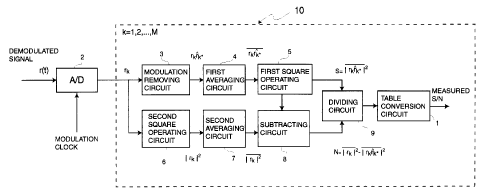
Fig. 1 is a view showing an S/N measuring circuit in an
embodiment of the present invention. In Fig. 1, an S/N
measuring circuit 10 in the embodiment of the present
invention includes a modulation removing circuit 3
connected to an A/D converter 2, a first averaging circuit
4, a first square operating circuit 5, a second square
operating circuit 6 connected to the A/D converter 2, a
second averaging circuit 7, a subtracting circuit 8, and a
dividing circuit 9, and this arrangement is the same as
the first prior art shown in Fig. 4. The S/N measuring
circuit 10 in the embodiment of the present invention
further includes a table conversion circuit 1.
Next, operation of the S/N measuring circuit 10 in the
embodiment of the present invention will be explained.
Referring to Fig. 1 again, a demodulated reception signal
is sampled at a modulation clock by the A/D converter 2.
First, a series of sampled values of a modulated signal
that is an output from the A/D converter 2 are averaged
over a plurality of symbol sections in the first averaging
circuit 4, after a modulated component thereof is removed
in the modulation removing circuit 3, and an amplitude
value in which a noise component is suppressed is obtained.
An output of this averaging circuit 4 is squared by the
first square operating circuit 5, and desired signal power
S is obtained.
CA 02243133 1998-07-10
- 20 -
On the other hand, an output of the A/D converter 2 is
supplied to the second square operating circuit 6, and is
converted into time series having a dimension of electric
power. Thereafter, the output is averaged over a plurality
of symbol sections by the second averaging circuit 7, and
total electric power P of demodulated signals is obtained.
The subtracting circuit 8 obtains noise electric power N
by subtracting the desired signal power S from the total
electric power P of the demodulated signals.
Although the operation so far is the same as that of the
conventional S/N measuring circuit shown in Fig. 4, in the
S/N measuring circuit in the present invention, the table
conversion circuit 1 is provided behind the dividing
circuit 9, and converts an S/N output from the dividing
circuit 9 and outputs it. In the table conversion circuit
1, as shown in Fig. 2, characteristic that is the reverse
of non-linear bias characteristic of the S/N output from
the dividing circuit 9 is stored as a table, and the
table conversion circuit instantly outputs an S/N value in
which a bias is corrected. Thereby, correct S/N
measurement becomes to be possible.
Also, Fig. 3 is a block diagram showing a transmitting
electric power control apparatus using the S/N measuring
circuit 10 in Fig. 1. In Fig. 3, a base station 20
includes an A/D converter 2, an S/N measuring circuit 10,
CA 02243133 1998-07-10
- 21 -
a demodulator 11 connected to an antenna, a decoder 12, an
adder 13, a decision device 14, a TPC bit generating
circuit 15, and a transmitter 16 connected to an antenna.
Also, a mobile station 53 like the prior art includes a
demodulator 21, a TPC bit decoder 22, a transmitting
electric power determining circuit 23, a transmitter 24,
and an encoder 25.
Operation of the transmitting electric power control
apparatus of Fig. 3 will be explained. First, in the base
station 20, demodulated signals demodulated by the
demodulator 11 are sampled at a modulation clock by the
A/D converter 2. A series of sampled values of the
demodulated signals that are outputs of the A/D converter
2 are input to the decoder 12, and, after an error is
corrected and the signals are decoded, information signals
are obtained. In digital mobile communication, although,
in order to improve communication quality, coding and
error correction decoding processes are generally applied
to the information signals, the present invention includes
the case in which these processes are not used. On the
other hand, an output of the A/D converter 2 is supplied
to the S/N measuring circuit 10. The S/N measuring circuit
10 in Fig. 3 has the same arrangement as the S/N measuring
circuit 10 shown in Fig. 1, and has a function in which a
corrected and accurate S/N value is measured from the
CA 02243133 1998-07-10
- 22 -
sampled value of the demodulated signal and output. In the
adder 13, a difference between a measured S/N that is an
output from the S/N measuring circuit 10 and a preset
control target S/N of transmitting electric power is
calculated and supplied to the decision device 14. The
decision device 14 determines an amount of increase or
decrease of the transmitting electric power to the mobile
station 53, based on an output from the adder 13. The
determined amount of the increase or decrease of the
transmitting electric power is converted into a bit by the
TPC bit generating circuit 15, and is transmitted to the
mobile station 20 by the transmitter 16.
In addition, in the embodiment of the present invention,
with regard to the control target S/N of the transmitting
electric power, the control or the like using the target
S/N control circuit 52 as shown in Fig. 5 is not conducted.
On the other hand, in the mobile station 53, the
demodulator 21 receives a signal transmitted by the base
station and conducts demodulation. A demodulated signal
that is an output from the demodulator 21 is input to the
TPC bit decoder 22, and the TPC bit decoder decodes the
TPC bit generated in the base station 20. The TPC bit
decoded in the TPC bit decoder 22 is input to the
transmitting electric power determining circuit 23, and
transmitting electric power of the mobile station 53 is
CA 02243133 1998-07-10
- 23 -
determined. In accordance with the transmitting electric
power determined by the transmitting electric power
determining circuit 23, the transmitter 24 transmits a
coded information signal.
As explained above, in the present invention, non-linear
bias characteristic in the S/N measurement is previously
obtained by measurement, the conversion table for
realizing this reverse characteristic is created, and when
a measured S/N value is output from the dividing circuit,
the table conversion circuit receives this S/N value as an
input and outputs a corrected S/N value from the above-
described conversion table. Therefore, it is possible to
provide the S/N measuring circuit capable of measuring the
S/N with high accuracy.
Also, in the digital mobile communicating system of the
present invention, the above-described corrected and
measured S/N is compared with the target S/N in the base
station, and the base station transmits a demand for
increasing and decreasing the transmitting electric power
to the mobile station, and, in accordance with the
instruction from the base station, the transmitting
electric power is determined in the mobile station.
Thereby, it is possible to provide the digital mobile
communicating system and the base station thereof, in
which it is not necessary to control the target S/N value
CA 02243133 2002-10-17
74790-25
- 24 -
separately, and transmitting electric power control can be
simply realized with high accuracy.
Furthermore, in the present invention, since the outer-
loop for correcting an S/N measuring bias is not necessary,
a scale of the apparatus becomes to be small. Also, since
the apparatus can cope with a fast change of the received
S/N, it is possible to provide the transmitting electric
power control apparatus capable of conducting the
transmitting electric power control with high accuracy.