Note: Descriptions are shown in the official language in which they were submitted.
CA 02243213 1999-O1-OS
- 1 -
The invention relates to an electrically screening housing for
accommodating and electromagnetically screening assemblies
which emit electromagnetic radiation or are sensitive to
electromagnetic radiation.
It is known to make electrically screening housings from
electrically non-conductive material, particularly plastics,
by coating the prefabricated housing parts with a conductive
material, e.g. by spraying them with conductive lacquer or
applying aluminium by vapour deposition (cf.
"Kunststoffgehause and EMV", elektronikindustrie 3 - 1992, p.
42). Such housings were generally provided with prefabricated
seals made of conductive elastomer which were put in place
during assembly. DE 38 12 943 A1 discloses an internally
coated screening housing of fibre-reinforced plastics with a
prefabricated seal of this kind placed between the groove and
tongue.
Housings of the type described above - which have achieved
particularly marked economic significance with the rapid
proliferation of mobile telephones - are also known from EP
0 629 114 B1 and EP 0 654 962 A1.
The housings described therein are made up of two parts which
consist of electrically conductive material or are coated with
such for the purpose of electrically screening the inside of
the housing (at least in parts) and in the assembled state
26806-24
CA 02243213 1999-O1-OS
- 2 -
form a Faraday cage. For electromagnetically screening the
housing in the area of the join between the adjoining housing
parts there is also a screening seal which consists of an
electrically conductive and at the same time elastic material
and adapts to surface tolerances and unevenness, so that a
very high quality screening of the inside of the housing can
be ensured even with large-scale mass production. According
to the specifications referred to above, this screening seal
is produced directly on at least one of the housing parts,
whilst an additional carrier may also be included in the
construction.
By virtue of this construction the housing is easy to open,
e.g. for maintenance purposes or for changing a battery in the
housing, and is easily resealed afterwards whilst retaining
the screening effect.
However, when producing a material for the screening seal, it
is difficult for certain applications to achieve the best
possible compromise between high elasticity, high conductivity
and lowest possible material costs. A material which is
advantageous from the physical point of view is a plastics
composition filled with a high proportion of silver powder,
but this is relatively expensive.
The aim of the invention is therefore to provide an
electrically screening housing of the type mentioned
26806-24
CA 02243213 2001-09-28
27107-6
2a
hereinbefore which is cheap to manufacture.
The invention provides an electrically screening
housing for accommodating and providing electromagnetic
screening of a component or module that emits
electromagnetic radiation or that is sensitive to
electromagnetic radiation, said housing comprising: a first
housing part having means for electromagnetic shielding; a
second housing part made of plastic materials and a first
sealing element disposed between the first and second
housing parts, the first sealing element being connected to
the second housing part and being made of a material that is
essentially non-conductive electrically, the first sealing
element and second housing part forming a unitary structure
that abuts the first housing part at a joint, wherein the
unitary structure additionally includes a second sealing
element that is disposed adjacent the first sealing element,
and an electrically conductive coating that extends at least
over the joint and that adheres to the first sealing element
and the second housing part, and wherein the conductive
coating additionally extends between the first and second
sealing elements.
From another aspect, the invention provides a
method for producing an electrically screening housing for
accommodating and providing electromagnetic screening of a
component or module that emits electromagnetic radiation or
that is sensitive to electromagnetic radiation, the housing
including a first housing part having means for
electromagnetic shielding, a second housing part made of
plastic material, and a sealing element disposed between the
first and second housing parts, the sealing element being
connected to the second housing part and being made of a
material that is essentially non-conductive electrically,
CA 02243213 2001-09-28
27107-6
2b
the sealing element and second housing part forming a
unitary structure that abuts the first housing part at a
joint, the unitary structure additionally including an
electrically conductive coating that extends at least over
the joint and that adheres to the sealing element, said
method comprising the steps of: molding the second housing
party forming the sealing element on an edge region of the
second housing party applying the conductive coating to the
second housing part and the sealing element; and joining the
first housing part and the unitary structure, wherein the
sealing element is not formed from the same type of plastic
material that the second housing part is molded from, and
wherein the steps of molding the second housing part and
forming the sealing element are conducted simultaneously in
a single-stage injection-molding process.
The invention also provides a method for producing
an electrically screening housing for accommodating and
providing electromagnetic screening of a component or module
that emits electromagnetic radiation or that is sensitive to
electromagnetic radiation, the housing including a first
housing part having means for electromagnetic shielding, a
second housing part made of plastic material, and a sealing
element disposed between the first and second housing parts,
the sealing element being connected to the second housing
part and being made of a material that is essentially non-
conductive electrically, the sealing element and second
housing part forming a unitary structure that abuts the
first housing part at a joint, the unitary structure
additionally including an electrically conductive coating
that extends at least over the joint and that adheres to the
sealing element, said method comprising the steps of:
molding the second housing part; forming the sealing element
on an edge region of the second housing party applying the
CA 02243213 2001-09-28
27107-6
2c
conductive coating to the second housing part and the
sealing element; and joining the first housing part and the
unitary structure, wherein the sealing element has a
predetermined shape after the forming step is conducted, and
wherein the method further comprises the step of deforming
the shape of the sealing element before the step of applying
the conductive coating is conducted.
The invention includes the technical teaching of
not making the screening seal entirely from an electrically
conductive and at the same time flexible material, in order
to save costs, but of filling the joint using an element
formed on site from electrically substantially non-
conductive but ductile (elastic) material and achieving the
electrical screening in the area of the
CA 02243213 1998-07-16
- 3 -
join by means of a layer of electrically conductive
material adhering to this element and merging seamlessly
into the screening of the substantially rigid walls of
the housing.
The sealing element primarily has the function of
filling the interstice of the join so as, for example,
to reliably protect the inside of the housing from
moisture and dust, in the event of any mechanical play
between the housing parts caused by manufacturing errors
or surface unevenness, and to prevent relative movements
between the housing parts. As a result of the improved
mechanical properties of the sealing mass it is thus
possible to provide a durable hermetic seal for the
inside of the housing. At the same time the sealing
element naturally carries part of the electromagnetic
screening and ensures that it is sealed. It is
particularly advantageous in this respect to use a high-
grade elastic material and/or a flexibly shaped seal by
means of which a prestress is built up between the
housing parts during the assembly of the housing parts
by the compression and/or bending of the sealing
element, capable of preventing the undoing of a screw or
clamp connection. However, the invention is not
restricted to the use of carrier elements which are
elastic by their material and/or shape, but can in
principle also be performed with a plastically
deformable sealing element.
In the preferred embodiment of the invention, the
covering consisting of electrically conductive material
is applied cohesively (and particularly in a single
operation) to the surface of the sealing element and the
rigid housing wall.
In another alternative embodiment of the invention the
screening is of a sandwich construction, the carrier
CA 02243213 1998-07-16
- 4 -
element consists of at least two layers of electrically
non-conductive but flexible material between which is
provided the layer of electrically conductive material
which brings about the electromagnetic screening. The
arrangement of the layer of electrically conductive
material in a substantially deformation-free area
between two deformable layers or strips of the elastic
element advantageously counteracts cracking in the
electrically conductive material, which is particularly
important for constructions in which severe deformation
of the screening element is supposed to occur or may
occur when the housing parts are put together.
In another advantageous embodiment, it is proposed that
the layer of electrically conductive material be made
very thin in order to prevent cracking, since the
bending stresses and hence the tendency to cracking
increase as the layer thickness increases for a given
amount of bending. The thickness of the layer of
electrically conductive material is therefore
substantially less (preferably by one to three orders of
magnitude) than the width of the join.
The application of the screening layer to the sealing
element or - in the case of a sandwich construction - to
one layer or strip thereof may be effected by various
methods. Suitable methods of achieving uniform layer
thicknesses are the processes known per se of spraying
with conductive lacquer or spraying with a pure metal,
but particularly galvanic metallisation and the
processes of gas phase deposition (known especially from
the manufacture of electronic components) such as
sputtering and CVD (chemical vapour deposition).
In an advantageous embodiment, within the scope of the
processes mentioned above, the coating is produced by
the controlled growth of crystallites in accordance with
CA 02243213 1998-07-16
- 5 -
the structurally predetermined directions of mechanical
stressing of the substrate (especially the sealing
element). Small lamellar surface elements may be formed
on the surface - particularly in a multilayered
structure - which cohere only loosely within the layer
and are thus movable relative to one another to some
extent during bending of the carrier element, which
also counteract any cracking in the screening layer. It
is particularly favourable if said crystallites are
arranged in the manner of scales or roof-tiles, which
can be achieved by angled spraying or sputtering of a
suitable substrate with an appropriate choice of the
coating parameters, i.e. apart from the orientation of
the substrate, the substrate temperature, the flow rate
of the gas, etc.
In another alternative embodiment of the invention the
application of the electrically conductive layer to the
carrier element is not carried out in the mechanically
tension-free state but in a state of predetermined
compression and/or bending of the sealing element. This
ensures that cracking in the electrically conductive
layer does not lead to a reduction in the
electromagnetic screening action of the screening
element. In this embodiment, the invention starts from
the idea that cracking in the electrically conductive
layer is difficult to prevent under all circumstances
owing to the deformation of the screening element which
occurs during the assembly of the housing, which means
that it is important to minimise the negative effects of
such cracking on the electromagnetic screening
characteristics. As a result of the application of the
electrically conductive layer in the deformed state of
the sealing element cracks may possibly form
subsequently when the tension is released, and these are
substantially closed up again during the later
deformation of the sealing element caused by the
CA 02243213 1998-07-16
- 6 -
assembly of the housing, as the sealing element will
then assume substantially the same form as it does
during the application of the conductive layer.
Other advantageous features are recited in the
subordinate claims or described more fully hereinafter
together with the description of the preferred
embodiment of the invention, with reference to the
drawings, wherein:
Figure 1 shows, as a preferred embodiment of the
invention, a housing made up of two housing parts for
electromagnetically screening an electronic circuit,
shown in exploded view,
Figures 2a and 2b are cross sections through a part of
the wall of the housing in Figure 1 in the region of the
join between the housing parts according to two
different embodiments,
Figure 3 shows another embodiment of the housing in
Figure 1, again viewed in cross section, and
Figures 4a and 4b show a cross sectional view of a
housing portion in another embodiment (a) with the
sealing element tension-free and (b) with the housing in
the assembled state.
Figure 1 shows a housing 1 for an electronic circuit C
which screens said circuit electromagnetically. On the
one hand this prevents the circuit C from suffering
interference from electromagnetic radiation coming in
from outside, so that the circuit 1 can operate even in
conditions subject to serious electromagnetic
interference. On the other hand, the screening may
prevent the electromagnetic radiation produced during
operation from coming out of the housing, which might
CA 02243213 1998-07-16
-
cause interference in the environment or present the
possibility of unauthorised knowledge of functions
occurring in the circuit.
The housing consists of a tub-shaped lower part 2 having
a rectangular cross section of opening and a plate-
shaped cover 3 for closing off the lower part 2 and
comprises a seal 4 formed directly ("dispensed") on the
lower part 2 to seal the join between the lower part 2
and the cover 3. The cover 3 is attached to the lower
part 2 by screwing, with four screws 5.1 to 5.4 passing
through corresponding bores in the corners of the cover
3 and screwed into screw threads in the lower part 2.
Both the lower part 2 and the cover 3 are injection
moulded from plastics, and all the inner surfaces -
including the surface of the fitted seal 4 - are
provided with a conductive coating 6.1 or 6.2 (which is
cohesive for each housing part). The coatings 6.1 and
6.2 are in electrical contact with one another when the
housing 1 is screwed together, and form an
electromagnetically screening Faraday cage.
Thus, as is apparent from the cross sectional view shown
in Figures 2a, the screening seal consists of a
resilient sealing element 4 made of a conventional
elastic plastics material (such as unfilled silicon or
neoprene) adhesively attached to the lower part 2, and
the associated portion 6.1a of the conductive coating
6.1 (e.g. of sprayed on aluminium, copper or Cr-Ni or a
one- or multi-component galvanic coating). As shown in
Figs. 4a and 4b, a layer of adhesion promoter known per
se but matched in its physical properties to the
resilient sealing material may also be provided.
Fig. 2b shows as the housing 1' a modification of this
housing in which both housing parts 2', 3' have a
CA 02243213 1998-07-16
_ g _
galvanic coating 6.1' or 6.2' all over them, and enclose
the seal 4' previously pressed onto the lower part 2'
and hardened thereon, while adhering thereto, by the
flow of air or by hot vulcanisation.
In another modification (not shown) the seal is
extruded, together with one of the housing parts, from
two different polymers, the monomers used being matched
particularly in terms of the extrusion parameters and
their thixotropic qualities as well as the temperature
and rate of cross-linking.
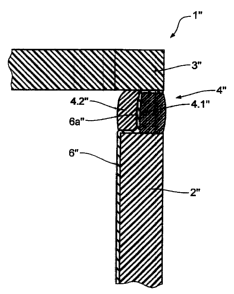
Fig. 3 shows as another embodiment a housing 1" which
externally resembles the housing in Fig. 1, and which
also has a lower part 2" consisting of an extrusion
moulded plastics material, but the cover 3" of which is
made from solid aluminium sheet. Therefore, there is
only a metal coating 6" on the lower part. This coating
also covers a sealing strip 4.1" mounted in the region
of the outer surface of the lower part. A second sealing
strip 4.2" dispensed close to the inner edge of the
lower part in a separate application step after the
application of the metal layer completes the seal 4".
The seal thus has a sandwich structure in which the
conductive coating is substantially freed from the
tensile forces resulting from the deformation of the
seal as the housing is closed and therefore the risk of
cracking in the screening layer is largely eliminated.
The arrangement of the conductive section 5a" of the
layer in the centre between the two strips 4.1", 4.2" of
the sealing element is advantageous inasmuch as the
mechanical bending stress of the coating in this case is
minimal under the monaxial compressive stress which
occurs as the housing is screwed together, thereby
reducing the danger of cracking. Cracking is made even
more unlikely by the mechanical fixing of the
electrically conductive layer between the two layers of
CA 02243213 1998-07-16
- 9 -
the sealing element.
This objective can be achieved - at least to a certain
extent - in the simpler structures of Figs. 2a and 2b by
keeping the thickness of the metal coating to a minimum
compared with the dimensions of the seal. Depending on
the size of the housing, the manufacturing tolerances
which have to be taken into consideration and the
screening action required, it may advantageously be
fixed at as little as a few tens of microns or even just
a few microns. This also shortens the process -
particularly when producing a very pure and,
advantageously, highly conductive layer by a vapour or
vacuum process - and reduces the costs.
A special layered structure with a reduced tendency to
cracking is shown in Figs 4a and 4b (in the tension-free
state and in the assembled and hence deformed state,
respectively).
Here, a lower housing part 20 as well as a lip-like
elastic sealing element 40 comprises an adhesion-
promoting layer 61 and a metallic coating 62, the latter
being produced, for example, by the oriented growth of
crystallites on the surface in a vacuum process. The
crystal growth is controlled so that, on the surface of
at least the sealing element 40, small scale-like
surface elements are formed which overlap with one
another to cover the surface almost completely and are
movable relative to one another to some extent (cf. the
enlarged diagrammatic detail "A" in Fig. 4a). This
prevents the electrically conductive coating 62 from
tearing apart when the housing is assembled as a result
of the deformation of the seal 40 caused by assembly,
which would lead to a deterioration in the
electromagnetic screening action. Rather, the layer
elements are monaxially oriented in overlapping manner
CA 02243213 1998-07-16
- 10 -
under the pressure of the metal cover 30 and the action
of the tensile force resulting from the bending of the
cross sectional profile when the cover is closed, and
form a continuous layer (cf. detail "B" in Fig. 4b).
The lip-like shape of the sealing element 40 which is
subjected primarily to bending stress during the
assembly - as shown in Fig. 4b - is specially chosen in
view of the structure of the layer 62 mentioned above.
This layer structure does, however, develop a similarly
beneficial effect on a substantially circular or
semicircular sealing profile subjected primarily to
compression, since once again the circumference will be
enlarged as a result of the deformation, and the scale-
like structure expanded as a result will then ensure
that the coating remains sealed even in the assembled
position of the housing.
The invention is not restricted in practice to the
preferred embodiments described above. Rather, a number
of alternatives are possible, making use of the solution
described even if the embodiments are of a fundamentally
different nature.
Thus, in technologically simple manner, a thin lip
standing in a C-shaped configuration in cross section
(as in Fig. 4a) on the housing part and typically formed
by injection moulding of a plastics housing part may act
as both the sealing element and the gap screening means,
by virtue of its elasticity of shape, if it is left on
the housing part and provided with a metal coating
together with said housing part. The sealing lip need
not necessarily be formed without a break along the edge
of the housing part.