Note: Descriptions are shown in the official language in which they were submitted.
CA 02243303 1998-07-16
-1-
BIT SLICED DIGITAL CROSS CONNECT SWITCHING SYSTEM
Technlcal Fleld
This invention relates to communication switching.
Baek~round of the Inventlon
s In prior art teleco",munication switching systems that
communicated a large number of calls, the reliability of the
telecommunication switching system has atways been a major problem.
Within the prior art, the solution to this reliability problem has been to fullyduplicate the system so that there is an active switching system and a
star,dby switching system. If a failure occurs in the active
telecommunication switching system, then, the standby
telecGmmunication switching system will commence to communicate the
active calls. Normally, the standby telccDm~unication switching system
performs this operalion with minimal disruption of active calls.
Whereas the prior art telecommunication s~itching systems
did provide a solution, this solution has many problems. The first pr~,e. "
is that the full duplication of the switching fabric adds a great amount of
cost and complexity to the resulting system. Further, the added reliability
achieved by having a fully duplicated system is not as great as would be
desired. The roason is that it takes one failure to ~ffeAblQ the active
switching network and only a second failure to disable the second
switching network. The re~ult is that two failures can cause a total failure
of the telecommunication switching sy~tem.
Summar~ of t~e Inventlon
The foregoing problems are solved, and a technical advance
is achieved by an apparatus and method in which a switching network
comprises a plurality of independent switching units with each switching
unit switching one bit of each group of data from external data links
through a telec~",l"unication switching system. Advant~geol~sly, the
plurality of switching units is greater than the number of bits that must be
CA 02243303 1998-07-16
switched which increases reliability. This allows the extra switching units
to be utilized as repl =~e"lent switching units should a switching unit
actively switching a bit of the incoming data be disabled. Advantageously,
the sv.;tching units provide full broadcast switching of data from any
s individual external link to any number of the other external links.
Advantageously, a plurallty of port units terminate the
external links, and a plurality of control paths are provide from a central
controller to each of the port units. Each of the switching units
communicated one of the control paths. For control, each port unit
deter",ines a set of control information that is identical from a majority of
the control paths.
Other and further ~spectF of the present invention will
become apparent during the course of the following clesc-iplion by
reference to the acco""~anying drawing.
Brbf De~cripllon ot tho l:~rawlng
FIG. 1 illusb~tes, in block diagram form, a
telecommunication s,~:it~;~ing system in accorJance with the invention;
FIG. 2 illu~ales, in block dia~3ram form, a bit slice switching
unit;
FIG. 3 illu~bdtes, in block diagram form, a first type of
timeslot interchange (TSI) unit;
FIG. 4 illusbates, in block diagram form, a second type of
TSI unit;
FIG. 5 illusbales, in block diagram form, a TSI block of a first
25 or secor,J type of TSI unit;
FIG. 6 illustrates, in block dia~ram form, greater details of a
bit slice inle"ace unit and a port controller;
FIG. 7 illusbdles, in flow chart form, operations pe, ~ol "~ed by
a DPLL controller of a port controller in adjusting the frequency of a local
30 oscillator;
CA 02243303 1998-07-16
FIG. 8 illustrates, in block diagram form a port unit;
FIG. 9 illustrdtes~ in block diagram form a system timing
unit;
FIG. 10 illustr~ates, in block diagram form another
s embodiment of a system timing unit;
FIG. 11 illuslfates a timing diagram;
FIG. 12 illu~t~ates a logic diagram of a digital synthesizer;
and
FIG. 13 illustrates, in flow chart form operations performed by a system
o timing unit in providing an G~ler"al fre4uency for another switching
system.
Detlllled DeSCrlDtiOIl
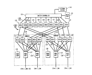
FIG. 1 illuslldtes~ in block diagram form a
telecommunic~tion switching system in accordance with the invention.
Switch co"t,cll~r 101 in response to i"~r",~lion received from main
co-lboller 100 corlt,ols the overall o~.er~liGn of the switching system
illuslldtecl in FIG. 1. The switching of data is pe,for",ed by bit sliced
switching units (BSSUs) 12~129. There are illustratively 10 BSSUs.
Each active BSSU switches one bit of each byte of each of the external
20 links such as link 103 con~ tecl to the switching system of FIG. 1.
Advantageousty link 103 and the other external links are STM-1 links.
Bilateral optical fiber links such as link 108 consist of one optical fiber
capable of communicating one bit ot data from each of 32 STM-1 links
between BSSUs and bit sliced inte,face (BSlUs) units. Since each BSSU
25 has eight inputs, BSSUs 120-129 are aapable of handling 256 STM-1
links terminating on the switching system illustlated in FIG. 1. At any
given time, only eight of the BSSUs 12~129 are in use. As will be
explained with l'eSpeCt to BSlUs 1 1 1-135, only eight of the BSSUs are
receiving data to be switched at any one time. Each BSSUis a self-
contained switching system that includes a full timeslot exchanger and all
CA 02243303 1998-07-16
required control memories to perform switching functions as set forth for a
full eight bit switching unit in U.S. Patent No. 5,416,772 which is hereby
incorporated by reference. In addition, each BSSU has associated with it
one BSIU from each of the subracks. Each BSSU, associated BSlUs, and
s interconnectin~ optical fiber links are t~r"~ed a switching group. As will be described in later paragraphs, the port controllers, such as port
controller 116, determine which bit from the STM-I links is to be
trans",ille.l to an individual BSSU based on control information received
frorn switch controller 101 Advantageously, a full timeslot interchanger
gives the switohing system of FIG. 1 the capability of doing full bro~st
switching. One skilled in the art could readily envision that other types of
switches could be used in place of a timesbt interchanger. In full
broAd~st switching, information received on an external link, such as
link 103, can be switched simultaneously to all outgoing communication
15 paths on the other e~-ler,-ai links. Greater detail on how a full time slot
interchanger is implemented in each BSSU is given in the s~tiGn which
details BSSU 120. Advantegeollsly, such full timeslot interchanging is
economically feasible by each BSSU ~witching only one bit from each of
the connected STM-I links.
ConsiJer now a BSIU, such as BSIU 1 11, of subrack 110 of
FIG. 1. BSIU 111 inlerco,.nects a bilateral optical fiber of link 108 with
BSSU 120. Similarly, BSIU 112 is interconnected by a bilateral optical
fiberwith BSSU 121. BSIU 111 onlyaommunicateswith BSSU 120.
Nob, that each of the two optical fibers for BSlUs 111 and 112 is carrying
25 a different bit from each of the 32 ST~1 links connected to subrack 110.
Subrack 1 10 has illustratively 32 port units each advantageously
terminating 1 STM-1 links resulting in 32 STM-1 links per subrack. One
skilled in the art could readily envision a port unit terminating more than
one STM-1 link. Each port unit l-ans"~it~ data on 1 transmit electrical link
30 to each BSIU and receives data on 1 ~cei~e electrical link from each
CA 02243303 1998-07-16
BSIU.- There is one pair of electrical links for each STM-1 link. For
example, port unit 117 has a transmit and receive link to each of
BSlUs 111-1 15. The result is that there are 320 electrical links in each
direction interaonnecting the port units to the 10 BSlUs of subrack 1 10.
5 Internally, each port unit can transmit any bit of each byte of a received
STM-1 bit stream on any of the l,ansn~il electrical links connecting to the
BSlUs. The el~,t~ ical links are indepe ~dent of each other. This allows a
port unit to distribute any individual bit to any of the 10 BSlUs. BSIU 111
is responsive to the bit stream being l~7cei-,red from each port unit to
10 combine and output these bit streams over optical fiber link 108 to
BSSU 120. Since the port units are capabb of transmitting any bit of the
incoming bytes to BSIU 111, BSSU 1~0 can be switching any of the eight
data bits of the incoming STM-1 links. Note, that all port units have to be
sending the same bit po.sition of the inco."i~ bytes to BSSU 120. This is
s neoessa, y sin¢e BSSU 120 returns this bit back to the port units after
switching the information so that the port units can l,ans",il this
information out on the int~r~Gn, ecting ST~1 links. The bits s~lQcted by
the port units of subrack 1 10 to be sent or received to or from a particular
BSIU is controHed by port conl,oller 116 based on information f~c~i~0d
20 from switch controller 101.
Since the port units can switch any bit of the bytes to any of
the BSSUs, if BSSU 120 fails, the bit that had been switched by
BSSU 120 can now be transfer,eJ to BSSU 129 or 128 (if these BSSUs
were inactive). BSSU 12~129 and their ~ssoc ~t~l BSlUs (switching
25 groups) are electrically and optically isol~t~l from each other; hence, the
switching system of FIG. 1 must suffer failures in three switching groups
before the system can no longer p6~ n the sv:itching of incoming bytes
on the STM-1 links. Further, since each BSIU switches only one bit and
there are ten BSlUs, three BSlUs of a ~iven subrack must fail before the
30 subrack can no longer switch information. Note, that the other subracks
CA 02243303 1998-07-16
-6 -
would still remain active. The only unit of the switching system illuslrated
in FIG. 1 whose failure can disable communication is a port unit and
failure of a port unit results in only one STM-1 link being unable to
communicate through the switching system illus~aled in FIG. 1. One
s skilled in the art could readily envision the use of a spare port unit to
further increase reliability.
In prior art systems, another source of system failure was
the failure to be able to communicate aontrol information. Within the
switching system of FIG. 1, switch controller 101 communicates control
10 information to BSSUs 120-129 via bilateral optical fiber links such as
link 104. Each BSSU communicates control information along with
switched data to and from the connected BSlUs. Each BSIU
communicates the control information b the port controller within the
subrack. Port controller 1 16 communi¢ates control information via
15 BSlUs 1 11-115. Port controller 1 16 transmits received control information
to port units 117-118. Re~use there are ten paths over which control
information can be communicated with switch controller 101, a port
controller is always guaranteed to have a valid control communication
path. Note, since each BSSU receives control information concer"ing its
20 operation through its own optical fiber link from switch controller 101, the
failure of such an optical flber only disables a single BSSU.
In a.J~i~iGn to control information being communicated over
each of the op~cal fibers i.~lerconnecting switch controller 101 to
BSSUs 12~12~, timing information is also communicated in this manner;
25 thereby, assuring that each BSSU receives its timing separat~ from other
BSSUs. In addition, each port controller utilizes timing information
received on all of the optical fiber links, such as link 108, from each BSSU
via t~he interconnecting BSIU and utilizes this timing information to assure
that the timing within the subrack conf~r,.,s to the timing of subrack
CA 02243303 1998-07-16
controller 101. Hence each port controller has multiple paths over which
timing information can be received.
FIG. 2 illu~it~dtes in greater detail BSSU 120. Each STM-1
link is communicating data as SDH frames, and each SDH frame has nine
s rows of data. BSSUs 120-129 switch data a row at a time. One skilled in
the art could readily envision switching a partial row at a time. BSSU 120
pe,for",s full SDH switching for one bit stream (also refer,ed to as a bit
position) of the bytes for each of STM-1 links illusbat~ on FIG. 1. The
connec~ions of BSSU 120 to the BSlUs of the subracks is via bilateral
optical fibers that terminate on optical transceivers 201-204. For example,
optical l,ansceiver 201 connects to oplical ffber link 108 from BSIU 111 of
subrack 110. Each of the optical fiber links from a BSIU is transporting
one bit stream of data for the 32 STM-1 links connected to a subrack.
Each row of da~a contains one bit from each ST~I link. Within a subrack
15 such as subrack 110 port unit 117 transmits to BSIU 111 one bit of a row
from the connected STM-1 link. Each subrack has a total of 32 port units.
BSIU 111 is responsive to the bits for each of the 32 ST~1 links to form
these bits into a single bit stream which is transmitted on link 108 to
BSSU 120.
Control and timing information is communicated by
BSSU 120 with switch controller 101 via optical filber link 104 which is
ter"~ at~l by optical l,anscciver and timing circuit 217. Circuit 217
communicates the control information on control bus 223.
The switching of data being received from the subracks via
25 optical hanscdi~ers 201-204 is peitor"~d by TSls 20~214. There are 16
TSls in each BSSU, and this allows the BSSUs to provide full bro~dc~st
switching. The TSls are grouped into pairs such as TSls 206 and 207.
Note, that TSls 208 and 209 TSls 211 and 212, and TSls 213 and 214
also form pairs of TSls. WHhin a TSI pair, one type of TSI receives data
30 from the optical fiber link and the other type of TSI transmits data on the
CA 02243303 1998-07-16
optical fiber link. Within a TSI pair each TSI performs the switching of
data to the int~rconnecting optical fiber link. For simplification of
nomenclature, these two types of TSls are refe"e,J to as a transmit TSI
and a receive TSI. Each pair of TSls has ~rcess to all of the bits being
5 received by other pairs of TSls. This i9 accomplished by the utilization of
pass links between TSls which allows the arculation of received data bits
from the eight optical fiber links inler~G~necting BSSU 120 to the
subracks 110-130. Pass links group 218 cG",prises 16 pass links pass
links 21~221. Each pass link cG",prises four bits. Each TSI pair
o transmits data received from its interconnected optical fiber link on two
pass links. For example, TSI 206 tran~mits on pass links 219 and 220 the
received data from optical transceiver 201. TSls 206 and 207 receive
data Assoc: ~1 with the other opffcal fibers terminated on optical
transceivers 202-204 on the remaining 14 pass links of pass links
15 group 218. As will be ~s~ il,e J with r~spect to FIG. 3 the recaiv;"g TSI
of the TSI pair torms the incoming data from the optical transceiv0r into
eight bit data streams. For example, TSI 206 is ~sponsive to the data
being received from optical transceiver 201 to forrn this into eight data bi
streams which are tra~-s",ill3 ~ on pass links 219 and 220 by TSI 206 .
20 Each stream of these eight data bit streams contain data from four STM-1
links. TSI 206 r~aives these eight bits of each data bit stream back
again after they have ,~ 9~ through TSls 207 through 214. TSI 206
does not continue to circulate the data bit ~l~ea",s.
Each TSI extracts four data bit streams from all incoming
2S data bit sbea",~ to BSSU 120. The rec~iving TSI transfers me results of
its extracting to the translr~iUing TSI. Each TSI pe. f~m~s full SDH
switching on each data bit stream with each data bit stream containing
data for four STM-1 links. For example, TSI 206 transfers the bits which it
has switched from the incoming data bits to TSI 207 via pair link 222.
30 TSI 207 is respoi 'sive to the four bits being received on pair link 222 and
CA 02243303 1998-07-16
the four bits that it has switched for each clock cycle to form these bits into
a single data bit stream that is then lr~sfer,ed to optical l.ansceiY0r 201.
The latter transceiver transmits this data bit stream on link 108.
PLL 224 provides the ne~essery timing of the incoming
s information on optical fiber link 104 and generates the internal timing of
BSSU 120. Circuit 216 I~ ~sse"lLles the control infor"~aliGn being
received from optical fiber link 104 into informaffon that must be
transfer,~ to port controllers and inforrnation that will be utilized to controlthe operalion of BSSU 120. Both types of information are placed on
diff rent bits of control bus 223. Similarly control information that is being
received by the receive TSls from the port controllers via the
interconnecting opffcal fib~r links is placed on control bus 223. Circuit 216
extracts this recei~ed control information from control bus 223 and
combines it with the SDH rows that ar~ being l-ans",itt~l out on optical
15 fiber link 104 to switch controller 101.
Consicler now receive TSI 206 as illustrated in FIG. 3. The
other receive TSls are id~ntical in desi~n. Data circuit 301 receives the
information from optical l.~sceiver 201 and provides the necess~ry
elastic storage function and timing reco~,ery so as to match the timing of
20 the receivcd data with the internal timing of TSI 206. One skilled in the art readily knows how to provide the functions of data circuit 301. Data
circuit 301 takes the serial bit stream and forms this into eight slower bit
sl.e~,ns that are transmitted synchronously on bus 300 to s~l~Gtors 303-
307. There ar~ si~-leen selectors. Each of the eight slower bit streams
25 contain data for four ST~1 links. Each sebctor is selecting four bits from
bus 300 or four bits from a pass link of pass links group 218. The
selectors are controllcd by scl~Gtor control 309 which is resl~onsive to a
TSI address being received on bus 308. The TSI address is permanent
for each TSI. Only two selectors are selecting bits from a data circuit at
30 any time in a receive TSI. In the present example of TSI 206 control 309
CA 02243303 1998-07-16
-10-
- selects the eight bits from data circuit 301 to be outputted on
seloctors 303 and 304 . The remaining selectors will each select four bits
from the pass links group 218. For example sel~ctor 307 receives the
four bits being transmitted on pass link 221. The outputs of selectors 303-
s 307 are transmitted to pass forward output circuits 311 -314 and delay
circuits 316-319. The outputs of circuits 311 -314 are transmill~l on pass
links which make up pass links group 302 to TSI 207. Note that TSI 207
is responsive to the four bits being received from pass forward output
circuit 312 to p~.~Gr", the same delay fun~ ~ons as will be cJe~criL~ for
o delay circuit 316 of TSI 206. Data circuit 301 also extracts the control
information coming from the port controller which is destined to be
transmitted out on optical ffber link 104 to switch controller 101. This
control information is inserted onto control bus 223 and is properly
combined by circuit 216 of FIG. 2 into the inlorl"~tio" being transmitted on
5 optical fiber link 104.
The function of delay circuits 316-319 is to properly align
the 8 bits being received from data circuit 301 and the remaining 56 bits
from pass links group 218. This is necessary since the eight bits that are
received by TS~ 208 of FIG. 2 which are thon l,a,)sferl~J via TSls 20~214
20 to TSI 206 are delayed 15 inter"al clodk cycles as co",par~J to the data
that data circuit 301 is ba.r~s~er,i,)g to s~lectors 303 and 304. Since the
amount of delay for each delay block u~ ,~nds on the position of the TSI
relative to othef TSls in FIG. 2, the TSI address is also utilized to control
delay circuits 31 ~319.
The outputs of the delay circuits 31 ~319 are fed into TSI
group 320 which coi"~.,ises TSI blocks 321-324. For simplicity of FIG. 3
it is not illusl.at~d that each of the four bits coming from each delay circuit
is connected to each of TSI blocks 321-324 of TSI group 320. Each of
TSI blocks 321-324 is responsive to the 64 incoming bits to perform a
timeslot inlerchange function and to output one bit to its ~ssoci~ted output
CA 02243303 1998-07-16
11 -
circuit of output circuits 326-329. For example, TSI block 321 transmits its
switched bit to output circuit 326. Output circuits 326-329 transfer their
four bits via pair link 222 to TSI 207. These four bits are combined with
the four bits that are the switched output of TSI 207. TSI 207 transmits
s the combined bits to optical transceiver 201 for transmission on link 108.
FIG. 4 illustrates TSI 207. Delay box 402-406 pe,for", the
same functions as delay blocks 316-319 of FIG. 3. TSI blocks 411-414
perform the same functions as TSI blocks 321-324 of FIG. 3. Pass
forward blocks 407~10 perform the same functions as pass forward
10 blocks 311-314 of FIG. 3. One skilled in the art could readily envision that
the TSls of FIGS. 3 and 4 could be one common inleg.~l~J circuit with the
unused portions simply being dic~b!ed depen~Jing whether the circuit was
being used as a recei~e or transmit TSI. The selection could be based on
information in the TSI a~W.ess. Data circuit 401 is responsive to the
outputs from TSI blocks 411-414 and the four bits being rec3ived via pair
link 222 from TSI 206 to p~. ~Gr", proper framing for l,a.)s",ission on
optical fiber link 108. In ~J~ilion, data circuit 401 combines the control
information that has been separated by circuit 216 of FIG. 2 and placed
on control bus 223 into the information being transmitted on optical fiber
20 link 108 to BSIIJ 111 using techniq.les well known in the art.
FIG. S illustrates, in block diagram form, TSI block 321 of
FIG. 3. TSI blocks 322-324 of FIG. 3 and TSI blocks 411-414 are
identical in design. The 64 bits of informaffon that is being generated
each clock cyc~e by delay blocks 316-319 are loaded into dual port
25 memory 502 under a~ ~ control of timeslot counter 501. After four
clock cycles, one bit of data for all 256 SThl-1 links of FIG. 1 has been
loaded into dual port memory 502. For each timeslot, timeslot
counter 501 is incremented until it retutns to zero and continues to be
incremented from zero on up. Counter 501 cycles once for each
30 multiframe beir~ received by BSSU 120. The conlenls of timeslot
CA 02243303 1998-07-16
RAM 503 are set by information received from control bus 223 which has
been transmitt~d to BSSU 120 from switch controller 101 via fiber optical
link 104. The manner is which this is loaded into TSI RAM 503 is well
known in the art. Each word in TSI RAM 503 defines for each timeslot
5 whieh of the words that were stored in dual port memory 502 from 64
input bits is to be selecteJ. Under control of TSI RAM 503 ROM 506
provides fixed patlen~ signal generation G~rdtiGns. The conlenls of TSI
RAM 503 and ROM 506 implement the full SDH switching funetion. The
seleeted 64 bit~ of dual port memory 502 and one bit from selector 508
o are sent to seleetor 504 which under eontrol of a portion of the word from
TSI RAM 503 selects one bit out of the 65 bits and l,ans",ils this single bit
on link 330 to output circuit 326 on Fl(3. 3. ROM 506 outputs 8 bits on
cable 507 to seleetor 508. The latter selector seleets one of these bits for
l,an~",ission to sel~ctor 504 in respon~e to control bits on bus 223 if
s ROM 506 is the data souree.
Since at any point in time eaeh TSI block in eaeh of TSI 20
- 214 of FIG. 2 has the same information and can output information from
any partieular STM-1 link for transmission on all STM-1 links, a full
broadeast switehing capa~lity is realized within BSSU 120. Henee
20 together BSSUs 120-129 provide a full bro43~ l eapability of all bits of
the STM-I links. Further any eombinal~on of full to partial bro~dc~ct
capability ean be provided from any number of STM-1 links to the
remaining ST~1 links. Advant~geo~l~y, this eapability is made possible
by bit slieing th~ functions performed by BSSU 12~129 into individual bit
25 sliees.
With r~spect to the broA~-st eapability, it is important to
realize that there are the equivalent of 63 E1 trunks being transported by
each STM-1 link. The lowest piece of data that can be switched in the
SDH switehing protocol is a E1 trunk. This means that one incoming E1
30 trunk can be switched to all other outgoing E1 trunks. This results in a
CA 02243303 1998-07-16
- large bro~dc~$t capabilities since one E1 trunk could be switched
to 16,127 other E1 trunks.
One skilled in the art could readily envision that whereas the
present embodiment descfibes the s~Atching for performing the SDH
s switching functions other protocol switching could be performed on the
incoming links.
Turning now to the manner in which timing is transfer,e.J
from the switch controller 101 to the port conlh~ rs. Each port controller
has ten paths over which timing inforrnation can be received from switch
10 controller 101. FIG. 6 illu~tlates these paths for port cont~c er 116.
FIG. 6 illust.dt~s the timing paths from bit slice control (BSC) 602 of switch
cont,e'l0r 101 to digital timing unit (DTU) 603 of port controller 116 in
subrack 110. The other subracks have similar DTUs. BSC 602 receives
the timing information from system timing unit (STU) 601.. BSC 602
lS t,ans",ils the timing information embedded with control information to the
BSSUs via links such as link 104. Digital phase loop (DPLL)
controller 608 in conjunction with the BSlUs such as BSIU 111 is
responsive to the timing information recovered from the links feeding into
the BSIU 111-BSIU 115 to c~lcul'-te an adJiuslmenl for local osciJlator 605
20 utilizing well known techniques. With this adjustment, the output of local
oscillat~r 605 is in phase and frequenay synchroni~aliGn with STU 601 of
subrack conl,dler 101 that defines the system frequency.
Digital phase loop (DPLL) controller 608 pe"Grl"s this
opor~tion by averaging the differ~nces of the phase and frequency of th
2s information being receivod by BSIU 111-115. DPLL conl,~ller uses this
average difference to control the output of local oscill~tsr 605 by supplying
information to oscillator adjustment cir¢uit 606 that adjusts Iscal
os~ tor 605. As clescribecl in the next paragraph even though the
transmission on the links l~etween BSC 602 and BSSUs 12~129 is based
30 on a common time base, phase noise occurs on the paths before
CA 02243303 1998-07-16
-14-
- extraction of phase and frequency information by the BSlUs bec~use of
the fact that a series of PLLs are utilized in each of the paths to DTU 603.
As illuslfat~ in FIG. 6 BSSU 120 is responsive to the
control information being transmitted on link 104 to first recover the
5 frequency bein~ transmitted on link 104 utilizing RPLL 623 for purposes of
storing the information in an elastic store. BSSU 120 for purposes of
internal timing ~enerates the timing information utilizing PLL 224. Data is
transmitted out from BSSU 120 via link 108 utilizing timing generated by
TPLL 621 which supplies the frequency for data circuit 401. Thus,
o BSSU 120 uses three PLLs in series r~sulting in some jitter of the basic
system timing.
The data t,~s",itted on link 108 is then framed by
framer 611 which utilizes a RPLL similar to RPLL 623. Framer 611
recovers the data being t~ns",itl~ on link 108 and places that in elastic
s store 614 utilizi~g an addrdss generated by elastic store write
counter 612. Note that framer 611 converts the single bit stream being
transmitted on link 108 into eight slower parallel bit streams that are
stored in elastic stores 614. Within each of the bit streams stored in
elastic store 614 is groups of data each of which is to t~e trans,r,itted out
20 on four of the STM-1 links interconnecled to subrack 110. On read out
switch 616 separates out from each of the data ~bealns stored in elastic
store 614 the data for the individual ST~1 links before transmitting this
information to the a~ priate port unit, such as port unit 117 in
subrack 110. These data streams are trans",itt~ via cable 626 to each
25 individual port unit. The information is read out of elastic store 614 under
control of elastic store read counter 617.
Transmitter 615 pe"or",s a similar Gperation as performed
by elements 612-617 except that it transmils data. Transmitter 615 is
responsive to outputs from individual STM-1 links received from port units
30 such as port 117 illusl.atecJ in FIG. 8. As illUStrdte1J in FIG. 8 switch 817
CA 02243303 1998-07-16
transmits the received information from the STM-I link received from
receive framer 803 after having separated it into individual data bit stream
for each of the BSlUs. For example transmitter 615 receives one such
data bit streams via lead 817 which is part of cable 627. Transmitter 615
s is responsive to the bit streams being receiv0d from cable 627 to form
these into eight bit streams with each of the eight bit streams containing
data for four ST~1 links. This information is transferred to framer 611 via
cable 628. Framer 611 then tldnslllils this intormation on bilateral optical
link 108 utilizing the system MFS signal and clock signals receivod from
o timing signal generator 604. Transmitter 615 transmits the in~or",alion to
Framer 611 ut~izing timing received from timing signal generator 604.
Framer 611 relays the information via optical fiber link 108 to data
circuit 401 of BSSU 120. Data circuit 401 utilizes an elastic store similar
to elastic store 614 to place the inform~ation received from transl.,itler 615
15 in synch,onization with the timing bein~ genera~ed by PLL 224. As will be
explained later, each port unit under control of BSC 602 makes the
~lec;~ion as to which BSIU each of the bit positions incoming on the STM-
1 link is to be transmitted.
Control information being l.dnsl"illecl from BSC 602 via the
20 BSSUs is separated out by the framers of the BSlUs, such as framer 611
and trans",itle~ to control recei~er 631 of DTU 603. Control receiver 631
chooses the control information which is identical from the majority of the
BSlUs 111 -115. Control receiver 631 sep~ ates the control information
inlenJ~J for DPLL controller 608 and t~ans;."its this information on
25 cable 632 to DPLL contrdler 608. Control receivor 631 extracts the
control information that controls the de6i5~nalio" of which bit positions of
the connected STM-1 links will be comlmunicated by the individual port
units to BSlUs 111 -115. This control information is transmitted to the port
units via cable 633. Advant~geously, the use of multiple control
30 information paths allows a simple hardware circuit such as control
CA 02243303 1998-07-16
.16-
receiver 631 to determine the final control information which allows quick
response to new control information.
The purpose of elastic store 614 is to allow the buffering of
the data being received from link 108 so that this data can be read out of
s the elastic store 614 and transmitted to the proper port units in
synchroni~alion with equivalent elements in other BSlUs in the subrack.
Elastic store write counter 612 is controlled by the frequency being
ge,~erated by the clock signal on lead 618 from framer 611 and the
system multiframing strobe (MFS) signal being transn~itlecJ on lead 619.
IO Framer 611 recovers these two signals from the timing information
embedded in the data being transmiKed on link 108. The system MFS
signal defines the start of each multiple frame of the data being
transmitted on link 108, and the clock signal d~nes the rate at which
frarner 611 pre~ent~ a new bit for each of the eight parallel data she~",s
15 being written into elastic store 614. System MFS signal from link 108
defines when elastic store write counter 612 should be zero. Similarly
elastic store read counter 617 is controlled by MFS signal being
transmitted on lead 638 and clock signal being l.dnsmitted on lead 639
from timing signal generat~r 604 of DTU 603. Timing signal
20 generator 604 is controJled by the output by local oscillator 605. If the
frequency and phase being generated by local oscillator 605 has been
identical to the frequency and phase of the osci"rtor utilized by BSC 602
of a switch controller 101 for a long period of time, the contents of elastic
store write counter 612 will be equal to illustratively half the maximum
25 count value when the MFS signal on lead 638 sets elastic store read
counter 617 to zero. This function is performed by DPLL controller 608.
This dif~erence in the cont~ts of elastic store write counter 812 and
elastic store read counter 617 is desis/~ed to allow for fluctll~tions in the
frequency being utilized by DTU 603 and the system frequency being
30 utilized by BSC 602 of switch controller 101.
CA 02243303 1998-07-16
Consider now in detail how DPLL controller 608 adjusts the
frequency of local oscillato- 605. On the occurrence of subrack MFS
signal, the cont~.'t~ of elastic store write counter 612 are sl-obecJ into
latch 613. Eadh of the BSlUs 112-115 has a similar latch to latch 613.
s DPLL controller 608 reads the conlenls of each of these latches in
response to the subrack MFS signal. DPLL controller 608 then
illustratively s~lLtract~ from each of the latch contenls half of the maximum
value that can be stored in elastic write counter 612. The resulting
number for each of the BSlUs 111-115 defines the dirference in the phase
o of local oscill~t~r 605 and the phase of the system frequency as
recovered from each individual BSIU from its incoming link from its
~ssoc;~l~ BSSU. DPLL controller 608 is responsive to these resulting
numbers to p~.fo"n the operations illu~l,dted in FIG. 7.
FIG. 7 illustr~a1es, in flow chart form, the steps performed by
DPLL controller 608 of DTU 603 illusll~t~J on FIG. 6 in adjusting the
frequency of local oscillator 605. Once the o~.er~lions are started by entry
into start block 701, d e.,-sion block 702 detorrnines if the time period has
elapsed for performing the cAIc~ tions to adjust the frequency of local
oscillator 605. Advantayeously, the time period is 1 msec. If the answer
20 iS no, ~Jec;sion block 702 is repe~ted If the answer in decision block 702
is yes, block 703 sclects the first BSIU listed as being available in the
avaWable list. The available list defines those BSlUs whose timing had
previously been determinod to be accurate. Next, block 704 reads the
error information ~ssoc;~d with the solected BSIU. This error
25 information is ~tained from the framer of the selected BSIU such as
framer 611 of BSIU 111. Decision block 706 deterl,lines if a link error had
been det~:t~cl on the link interconn~~ g the selected BSIU with its
~ssoci~t~d BSSU. If the answer is yes that an error was detected, control
is transfer,ed to block 709 which removes the selccted BSIU from the
30 available list. After execution of block 709, control is transf~r,ad to
CA 02243303 1998-07-16
- 18 -
decision block 712 whose operation will be described later in this
paragraph. Returning to decision block 706, if the answer is no decision
block 708 del~",ines if information from the ~ssooi~ted BSSU indicated
an i"lernal error in the ~ssoc~ted BSSU. This information is also
s obtained from framer 611. If the answer in decision block 708 is yes,
control is L,ar,sler,ed to block 709 whose operatiGns were previously
desc,il)ed. If the answer in decision block 708 is no block 711 adds the
value from the dirference Jatch of the selected BSIU such as ~ terdnce
latch 613 after subtra~ tin~ half of the maxirnum count of the elastic store
l0 write counter from this vaJue into a total which is being maintained for later
use. After execution of block 71 1, dec sion block 712 ~Jeter",ines if there
is another BSIU listed in the available list. If the answer is yes that BSIU
is selected and control is transferred back to block 704 by decision
block 712.
Returning to dec;sion block 712 if the answer is no
block 713 determines the average of the infor",ation from the latches of
the BSlUs that qualified by dividing the calcul~~ total by the number of
qualified BSlUs. Both of these numbers were C:~IGul~ted in block 711.
Using the average numbcr takes advantage of the fact that uncorrelated
20 noise dec~eases as the number of usable sources increases. Block 714
then utilizes this average number to calculate an adjustment value using
techniques well know in the art and ll~ls",lts the adjl,sl"~enl value to the
oscill~tor adju~tment circuit such as oscillator adjustment circuit 606.
Control is tran~ferred to cl~;sion block 716.
Decision block 716 dete-",ines whether the time has
elapsed for performing a st~listicAI screening test on the BSlUs in the
available list. If the answer is no, control is trans~er,ed back to decision
block 702. The st~lislicAI screening is advantageously performed every
ten msec. One skilled in the art could readily see that the st~'islic~l
30 screening could be pe"or "ed at ~ erenl intervals. If the answer is yes in
CA 02243303 1998-07-16
19
decision block 716, block 717 selects the first BSIU which advantageously
would be BSIU 111. Decision block 718 then calculates the standard
deviation from the average and determines whether the value read from
the di~erence latch of the selected BSIU is within the standard deviation
s from the average value which was calculated in block 713. If the answer
is no in ~JecisiQn block 718, the sel -ct6J BSIU is removed from available
list before control is transf~r-~J to decision block 722. Retuming to
decision block 718, if the answer is yes, block 719 adds the selected BSIU
to the available list before bansfer,ing control to decision block 722.
o Decision block 722 determines if there is another BSIU to be s~ti~Li~'ly
scroened. In the present example, the last BSIU to be screened will be
BSIU 115. If the answer is yes in deci8ion block 722, block 723 selects
the next BSIU and transfers control back to decision block 718. If the
answer in deci$ion block 722 is no, control is transf~r.ed back to decision
s block 702.
The discussion of FIG. 7 is in terms of selecting a BSIU
which has recovered a frequency from the optical ffber link with the
associated BSSU that is stable enough to be utilized to ~~'cu'~te the
adjust",enl for local oscillator 605. However, for example with respect to
20 BSIU 111, one skilled in the art readily see$ that what is being selevted is
the path cG",~rising optical fiber link 108, the inl~!J,ily of BSSU 120, and
port unit 1 17. It is this path from BSIU 1 11 to BSC 602 that is being
sel~cted and qualified.
FIG. 8 illustr~les port unit 1 17. The other port units are
25 similar in design. Data is transmitted out on STM-1 link 103 under timing
control of PLL 802 utilizing the STM-1 clock signal on lead 813 from timing
signal generator 604 of DTU 603. Note, the l,ansceiver is not illustrated in
FIG. 8 but is well known to those skilled in the art This transmission is
done utilizing well known techniques. Incoming data from STM-1 link 103
30 iS framed by receiver framer 803.
CA 02243303 1998-07-16
- 20 -
Of interest in FIG. 8 is the manner in which the remote
phase detection is performed so that STU 601 can be locked in phase
and frequency to STM-1 link 103 via port unit 1 17. The link frequency is
recovered by receiver framer 803 and transmitted to anti-aliasing
5 PLL 804. PLL 804 has a 50 Hz low pass phase transfer function and
communicates the resulting filtered signal as a digital clock signal to
counter 805. In addition PLL 804 llai~s,nik~ to remote phase
controller 809 information concer"ing whether there is exGessive jitter or
loss of clock on the incoming link via cable 811. Counter 805 is a free
o running counter which simply counts up and returns to zero. The output
of counter 805 is latched into latch 806 under control of the MFS signal
received via lead 638 from timing sign~l generator 604. The MFS signal
occurs every 500 microseconds and is transmitl~d on lead 638 of FIG. 6.
The SUf~MFS signal is the MFS signal reduced by a multiple of 17 and is
15 transmill6J on lead 812. The previously latched data from latch 806 is
clocked into latch 807 by the MFS signal. Subtractor 808 calculates the
~Jifi~r6nce between the contents of latches 806 and 807. The difference
bel~reen Iatch~s 806 and 807 represents the number of input clock
periods which occurred during the last MFS interval. An exl ~1ed
20 ~Jift~r6nce number is then used to reduce the number of bits that must be
lrans",ill~J by remote phase contlcllar 809. The exl~ct6~J differencé
number is the number of clock periods which could be e~-~.ect~J if
STU 601 is in perfect sy,~,ronization with the STM-1 link to which
STU 601 is synching. It is this expect d ~ifference that is then subtracted
25 by sul~a~tor 808 from the difference between the contents of latches 806
and 807 to obtain a final d;fference. This final dMference is then used to
represent the incremental difference in phase in the 500 microsecond
inte~val betwe~n the link frequency and the frequency being generated by
local oscillator 605 of FIG. 6. Since the frequency of local osc ll~h~r 605 is
30 basically the system frequency generated by STU 601 and utilized to time
CA 02243303 1998-07-16
the system illust~aled in FIG. 1 the final diflere,)ce represents the
di~rence ~et~-~on link frequency and system frequency over one MFS
interval. This final ~Ifference is transmltted to STU 601 and is utilized by
that circuit to adjust the system frequency until the system frequency
5 matches the link frequency in phase and frequency.
Remote phase controller 809 forms a remote phase
mess~ge at the occurrence of each M~S signal. The remote phase
messAge consists of the present difference from subtractor 808 and the
sum of the di~.ences (also refer,ecJ to as the summation of differences)
that occurred over the last 16 cAIcu~lions. One skilled in the art could
readily envision that different sums could be calculated other than the
summation of the last sixteen calculalions. For exa,nple the sum of the
di~e.e,)ce that represented two c~lcu~q~ions could be calcu~te~ Further
one skilled in the art could readily envi~ion that a plurality of sums of
erences could be l,ans"~ilt~J in the re",ote phase mess~e at the
occurrence of each MFS signal. In addition, the messAge includes the
information transmitted via cable 811 from PLL 804 plus the conlenls of
counter 810. Counter 810 is a simple binary counter that counts to 16
and then reseb to zero. The contents of caunter 810 define the sequence
20 of the re",ote phase mes~Ages generated by remote phase controller 809.
The remote phase mess~es are trans!",itl1;J to DPLL controller 608 of
DTU 603 of FîG. 6. Each port unit is trans,r,itling unique but similar
remote phase messAges to DPLL controller 608. DPLL controller 608
under control of a mossAge previously receivcd from STU 601 selQcts
25 illustratively 0 1 or 2 of these rel"ole phase messAges and transmits the
selected remote phase m~ ge to STU 601 via each of BSlUs 11 1-1 15
and BSSUs 12~129. At any one time, STU 601 will only be using the
remote phase messages from one port unit. Advantageously, STU 601
can select two remote phase messAge~ from each subrack and up to
30 sixteen such remote phase messAges at any given time. One skilled in
CA 02243303 1998-07-16
the art could readily envision that this capability allows STU 601 to
pe~r", many types of synchronization operations. STU 601 makes the
ref~rence se'Qction based on which StM-1 links have been indicated as
having the ~re~lest accuracy of frequency. Such flexibility allows
s STU 601 to select any one of the 256 ST~1 links terminating on the
system illusl,ated in FIG. 1 as the link to which to adjust the system
frequency.
The data being received by port unit 1 17 from STM-1
link 103 is first framed by receive framer 803. Note that receive
o framer 803 includes the functions of the elastic store 614 and associated
write and read counters. Information is read out of the elastic store of 803
and lrans",itted eight bits parallel to switch 814. Switch 814 is responsive
to the bit slice control information from control lecehter 631 r~ceivcd over
cable 633 to form bit streams for the cable~ going to BSlUs 1 11-115. For
5 example, one bit stream would be transmitted via conductor 817 to
BSIU 111 if BSIU 111 was being utilized to switch data.
Data to be bdns",itt~l out on STM-1 link 103 is received by
switch 816 from each of the BSlUs 111-115 that is actively switching data.
For example switch 816 receives bits for one bit position of the STM-1
20 link via condudor 629 from switch 616 via conductor 629. In r~sponse to
control infor",ation being received frorn control receiver 631 via cable 633
switch 816 arranges the bi't posit;ons being recehred on the incoming
connectors so that they have the proper po~ition on the bits t)eing
l,ans",itt~l in parallel to transmitter framer 801 via cable 818. Cable 818
25 llanSpG-t3 eight bits in parallel. Transmit framer 801 is responsive to th
eight incoming bits received for each cycle to form these into a serial bit
stream for transmission on STM-1 link 103.
FIG. 9 illustrates in y,eal~r detail STU 601 of FIG. 6. The
remote phase messPges transmitted by remote phase controllers such as
30 remote phase controller 809 of FIG. 8 are ffrst received by BSC 602 which
CA 02243303 1998-07-16
transfers these to STU 601 of FIG. 6. DPLL controller 901 is responsive
to the remote phase mess~es from the se'Ected port unit to control local
osc;llator 904 with respect to phase via oscill ~tor adjustment circuit 903.
Local osci"~tor 904 is adjusted to precki~n oscillator 905 and the selected
s STM-1 link. The algorithm utilized by DPLL controller 901 to perform the
adjustment of local oscillator 904 is well known to a person skilled in the
art and is disclosed for example U. S. Patent No. 5 483 201 which is
incorpordt~J by reference. The output of local oscillator 904 is utilized to
drive timing signal generator 906 which provides the system timing to
o BSC 602.
FIG. 10 shows another embodiment of STU 601. In this
embodiment with respect to providing the system frequency for timing
signal generalar 1006 elements 1001-1005 function in an id~ntical
manner to elements 901-905 of FIG. 9. As in the first embodiment of
STU 601 of FIG. 9 DPLL co"t~oller 1001 is responsive to remote phase
mess~ges from a selected port unit to control local oscillator 1004. In
~dllition, physiGally located with the system illusllat~d in FIG. 1 is another
extemal switching system that needs to derive its system frequency from
another one of the STM-1 links. Since the trequency and phase of timing
20 signal generator 1006 is accurately represented down at each port unit
such as port unit 117, the r~",ote phase m~ s generated by ren,ote
phase cont~olle~r such as remote phase 809 of FIG. 8 can be utilized to
re~o Juce the frequency of any given STM-1 link by STU 601 utilizing
digital sy,lU,esi~ar 1012 of FIG. 10. DPLL controller 1001 is responsive to
25 the r6."~)te phase mess~s to control the number of pulses from timing
signal generator 1006 that are allowed to be transmitted to analog
PLL 101 1 by conlrollir,g digital synthesker 1012. Analog PLL 1008 is
responsive to the incoming pulses to reproduce an analog signal that is
highly accurate and filtered representalion of the frequency and phase of
CA 02243303 1998-07-16
the selected STM-1 link. This analog signal is then transmitted to the
external switching system.
FIG. 11 illuslrates the signals produced by the elements of
FIG. 10. Line 1 101 illu~ les the frequency signals outputted by timing
s signal generator 1006 on lead 1007. If the frequency and phase of the
line frequency signal is identical to the frequency signal outputted by
timing signal generator 1006 on lead 1007 for a long period of time, then
digital synthesizer 1012 continuously outputs the pulses illustrated on
line 1 103 of FIG. 11. The result is that for svery six pulses being received
lO from timing signal generator 1006 on lead 1007, digital synthesizer 1012
transmits to analog PLL 1008 on lead 1009 four out of the six pulses
being received on lead 1007. Analog PLL 1008 is responsive to these
pulses to produce advantageously a 2048 kHz signal which is transmitted
to the external switching system. If the line frequency of the STM-1 link is
lower than the ~requency of timing sigr~al generator 1006, digital
synthesizer 1012 under control of DPLL controller 1001 ~rljust~ for this
diff~rence in fr quency by producing three out of six pulses as illust~dled
in line 1 102 until the output of analog PLL 1008 matches the frequency
and phase of the STM-I link. Similarly, if the frequency signal of the STM
20 link is higher than the frequency of timing generator 1006, digital
synthesizer 1012 under control of DPLL controller 1001 l,ans",il~ five out
of six pulses for the inco,ning pulses being recei~eJ on lead 1007 as
illwtlat~ in line 1103. Analog PLL 1008 is res~nsive to these increased
number of pulses to raise the frequency of the signal being transmitted to
25 the exlernal switching system. The de~ign of analog PLL 1008 to be
responsive to digital pulses being recei~ed on its output to produce a
smooth and stable analog signal are well known to those skilled in the art.
FIG. 12 illust.ates the details of digital synthesizer 1012 of
FIG. 10. Elements 1201-1205 form a mod 6 counter that recycles after six
30 cloc~c pulses received on lead 1007 from timing signal generator 1006.
CA 02243303 1998-07-16
-25-
The design of mod 6 counters and their operation is well understood by
those skilled in the art and the details are not desclibed here.
Consideri,-g the overall operalion of the logic circuit illuslraled in FIG. 12
if flip flop 1214 is set then five pulses out of each cycle of the mod 6
s counter as illwt~dtecl on line 1103 of FIG. 11 being received on lead 1007
aretransfer,~tolead 1009viagates 1221 and 1222. Ifflipflop 1213is
set and flip flop 1214 is not then three of the pulses out of each cycle of
the mod 6 counter as illu~lr~l~J in line 1102 of FIG.11 are trans~er,~
from line 1007to line 1009viagates 1221 and 1222. If neitherflip
o flop 1214 or 1213 is set then four pulses out of the cycle of the mod 6
counter are transferred from lead 1007 to lead 1009 by gates 1221
and 1222. Gabs 121 ~1219 are res~onsive to the state of the mod 6
counter (outputs of flip flops 1201-1203) to control flip flop 1220 which in
turn conllols gate 1221 to acco",plish the previously desoril~d operations
with respect to flip flops 1213 and 1214. One ~killed in the art can readi~y
l,n~Jsr~land the operations of elements 1213-1222 in their relati~"ship to
flip l~ops 1201-1203 to perform these operations.
The state of flip flop 1214 is ~eter"~ined by the outputs of
shift register 1211 and the state of flip flop 1213 is determined by the
20 outputs of shift res;sler 1212 for each cycle of the mod 6 counter. Shift
registers 1211 and 1212 each contain eight bits. These eight bits are
inserted into the shift resisters via data and strobe signals received via
cable 1011 from DPLL controller 1001. Data to be loaded into shift
register 1211 is received via s~ hle 1225 and is loaded under control of
25 strobe signals on leads 1223 and 1224. Similarly, data to be loaded into
shift reg;ster 1212 is received via subcable 1226 and inserted into shift
register 1212 under control of strobe si~nals received on leads 1223
and 1227. ShiM res;~lers 1211 and 1212 are only shifted once for each
cycle of the mod 6 counter. This shiMil19 of bits within the shift registers is
30 controlled by gate 1206 and flip flop 1207 that allow the clock signal on
CA 02243303 1998-07-16
.26-
lead 1007 to shift the shift registers at the start of the cycle of the mod 6
counter.
FIG. 13 illusl-ates in flow chart form the steps performed by
DPLL cont~ollsr 1001 in controlling digltal synthesizer 1012. Deeision
s bloek 1301 debrmines if it is time to p~rform the ~Icul~tion of the
adjustment to be sent to digital synthesizer 1012. This C~IC~ tion is
performed advantageously every 8 msee. Reeall that the remote phase
controllers such as remote phase eontroller 809 of FIG. 8 ~Icul~te a
di~Jrenee between the system frequeney and the link frequeney every
o milliseeond but mai.)lain a sum of the ~ er~nees over an 8 msee period.
It is this s~,r""alion of di~f3renees that is utilized to adjust digital
synthesizer 101 2. If the answer is yes in ciesision bloek 1301 eontrol is
l,ans~er,~J to ~ecision bloek 1302 to deterrnine if an error oceurred in the
remote phase mes~ge If the answer is yes in ~ision bloek 1302
control is tran~fe-,ed to bloek 1303 for srror reeovery. If the answer is no
in ~Jec;sicn block 1302 eontrol is l,ansfer,e~l to ~beision bloek 1304 whieh
det~rmines if the summaffon of the .li~r~.el~es is greater than ~-7~ and
less than ~7". If the answer is no in deeici~1 bloek 1304 control is
l~ans~e"~J to bloek 1303 for error reeovery. If the answer in dseision
20 block 1304 is yes, d~;sion block 1306 det~rmines if the summation of the
di~erenees is bss than zero. If the an$wer is yes in deeision bloek 1306,
control is IrdnsfGrl~J to block 1307 whieh eonverts the absolute value of
the summation of .1i~6re"ees into the equivalent number of bits in a byte.
For example if the summation of diffo n nees was a '~' bloek 1307 would
2~ form a byte that had four 1 s and four as. After the byte is formed in
block 1307, eontrol is t.ansfer,ed to bloek 1308 whieh loads the formed
byte into shift ~eg;sler 1212 and inserts Os hto shift re~isler 1211.
Returning to dec;sio~ bloek 1306, if the answer is no
deeision bloek 1309 dete"-~ines if the summation of dif~ere,)ees is greater
30 than zero. If the answer is yes, bloek 1312 forms a byte whieh eontains
CA 02243303 1998-07-16
the equivalent number of bits equal to the absolute value of the
summation of differences. Block 1313 then loads this formed byte into
shift rey;ster 1211 and inserts Os into shift register 1212 before
l,a,-sfer,ing control back to decision block 1301. If the answer in decision
s block 1309 is no, control is transferred to block 131 1 which inserts Os into
shift reg.sters 121 1 and 1212 before transfoni~1g control back to decision
block 1301.