Note: Descriptions are shown in the official language in which they were submitted.
CA 02243451 1998-07-16
-1-
SYNCHRONIZING A CENTRAL TIMING UNIT TO AN EXTERNAL LINK
VIA A SWITCHING NETWORK
Technical Field
This invention relates to communication switching, and in
particular, to the synchronization of a timing unit to an external link.
Background of the Invention
In prior art telecommunication switching systems, it is well
known to synchronize a central timing unit within the telecommunication
switching system to an external link. Indeed, this is commonly done so as
io to maintain consistent timing throughout a public telecommunication
network. In prior art telecommunication systems, this was accomplished
by hardwiring timing links from one or more selected external links to the
central timing unit. The central timing unit then could select one of the
hardwired links to synchronize the internal timing of the central timing unit.
is Whereas the prior art telecommunication switching systems
did provide a solution, this solution has many problems. The first problem
is that the external links to which synchronization was to be performed
had to be selected and then, manually hardwired links had to be installed.
Because of the cost and complexity of establishing hardwired links,
2o normally only a small set of external links such as two were selected. In
addition, the hardwired links had to be duplicated for reliability purposes
but if the two duplicated hardwired links should fail, then the central timing
unit could not synchronize to that particular external link. In addition, new
international standards require that a telecommunication switching system
2s be able to determine which external link is connected to the best timing
source and utilize that external link. This means that a prior art
telecommunication switching system would have to have hardwired links
to each of the external links.
Summaryr of the Invention
CA 02243451 1998-07-16
-2-
The foregoing problems are solved, and a technical advance
is achieved by an apparatus and method in which local timing units
synchronized to a centralized timing unit determine the difference in timing
between external links and the local timing units. This difference in timing
s is then transmitted to the central timing unit, which utilizes this
information
to adjust the timing of the central timing unit. Advantageously, the
adjustment to the central timing unit brings it into synchronization with the
selected external link. Advantageously, the local timing units are
synchronized to the central timing unit via multiple timing paths set up
io through switching units within the network. Each switching unit switches
one bit of data for each group of data being received on each of the
external links. In addition, information received by each of the external
links designating the accuracy of the external link is transmitted to the
central timing unit so that the central timing unit can select the external
is link having the highest accuracy.
Other and further aspects of the present invention will
become apparent during the course of the following description by
reference to the accompanying drawing.
Brief Descrif~tion of the Drawing
2o FIG. 1 illustrates, in block diagram form, a
telecommunication switching system in accordance with the invention;
FIG. 2 illustrates, in block diagram form, a bit slice switching
unit;
FIG. 3 illustrates, in block diagram form, a first type of
2s timesiot interchange (TSI) unit;
FIG. 4 illustrates, in block diagram form, a second type of
TSI unit;
FIG. 5 illustrates, in block diagram form, a TSI block of a first
or second type of TSI unit;
CA 02243451 1998-07-16
-3-
FIG. 6 illustrates, in block diagram form, greater details of a
bit slice interface unit and a port controller;
FIG. 7 illustrates, in flow chart form, operations performed by
a DPLL controller of a port controller in adjusting the frequency of a local
s oscillator;
FIG. 8 illustrates, in block diagram form, a port unit;
FIG. 9 illustrates, in block diagram form, a system timing
unit;
FIG. 10 illustrates, in block diagram form, another
io embodiment of a system timing unit;
FIG. 11 illustrates a timing diagram;
FIG. 12 illustrates a logic diagram of a digital synthesizer;
and
FIG. 13 illustrates, in flow chart form, operations performed by a system
is timing unit in providing an external frequency for another switching
system.
Detailed Description
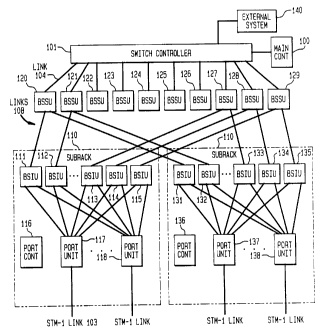
FIG. 1 illustrates, in block diagram form, a
telecommunication switching system in accordance with the invention.
2o Switch controller 101 in response to information received from main
controller 100 controls the overall operation of the switching system
illustrated in FIG. 1. The switching of data is performed by bit sliced
switching units (BSSUs) 120-129. There are illustratively 10 BSSUs.
Each active BSSU switches one bit of each byte of each of the external
2s links such as link 103 connected to the switching system of FIG. 1.
Advantageously, link 103 and the other external links are STM-1 links.
Bilateral optical fiber links such as link 108, consist of one optical fiber
capable of communicating one bit of data from each of 32 STM-1 links
between BSSUs and bit sliced interface (BSIUs) units. Since each BSSU
so has eight inputs, BSSUs 120-129 are capable of handling 256 STM-1
CA 02243451 2001-02-22
-4-
links terminating on the switching system illustrated in FIG. 1. At any given
time, only eight of the BSSUs 120-129 are in use. As will be explained with
respect to BSIUs 111-135, only eight of the BSSUs are receiving data to be
switched at any one time. Each BSSU is a self-contained switching system
that includes a full timeslot exchanger and all required control memories to
perform switching functions as set forth for a full eight bit switching unit
in
U.S. Patent No. 5,416,772. In addition, each BSSU has associated with it one
BSIU from each of the subracks. Each BSSU, associated BSIUs, and
interconnecting optical fiber links are termed a switching group. As will be
described in later paragraphs, the port controllers, such as port controller
116,
determine which bit from the STM-1 links is to be transmitted to an individual
BSSU based on control information received from switch controller 101.
Advantageously, a full timeslot interchanger gives the switching system of
FIG. 1 the capability of doing full broadcast switching. One skilled in the
art
could readily envision that other types of switches could be used in place of
a
timeslot interchanger. In full broadcast switching, information received on an
external link, such as link 103, can be switched simultaneously to all
outgoing
communication paths on the other external links. Greater detail on how a full
timeslot interchanger is implemented in each BSSU is given in the section
which details BSSU 120. Advantageously, such full timeslot interchanging is
economically feasible by each BSSU switching only one bit from each of the
connected STM-1 links.
In addition to providing control, switching controller 101 provides
all timing information for the system illustrated in FIG. 1. In general,
switch
controller 101 will be synchronized to one of the STM-1 links illustrated in
FIG. 1. Each port controller such as port controller 116 receives timing
information via each of the bit slice paths established through each pair of
BSSU and BSIU such as BSSU 120 and BSIU 111.
CA 02243451 1998-07-16
-5-
Because of the method of synchronizing the port controllers to switch
controller 101, each port controller is in excellent synchronization with the
central timing unit in switch controller 101. The port units receive their
timing information from the local timing unit in the port controller. In order
s to synchronize the central timing unit to an external link, each port unit
determines the difference in timing between the timing received from the
local timing unit and that of the connected STM-1 link. This difference
information, which is the difference in phase, is then transmitted to the
central timing unit. The central timing unit selects from the plurality of
io difference information being transmitted by the different port units and
utilizes the information associated with the STM-1 link to which the central
timing unit is to be synchronized. In addition, to sending difference
information, each port unit sends information defining the accuracy of the
connected STM-1 link with this information being received over the STM-1
is link. Utilizing this accuracy information, the oral timing unit can select
the STM-1 link having the most accurate timing.
Consider now a BSIU, such as BSIU 111, of subrack 110 of
FIG. 1. BSIU 111 interconnects a bilateral optical fiber of link 108 with
BSSU 120. Similarly, BSIU 112 is interconnected by a bilateral optical
2o fiber with BSSU 121. BSIU 111 only communicates with BSSU 120.
Note, that each of the two optical fibers for BSIUs 111 and 112 is carrying
a different bit from each of the 32 STM-1 links connected to subrack 110.
Subrack 110 has illustratively 32 port units each advantageously
terminating 1 STM-1 links resulting in 32 STM-1 links per subrack. One
2s skilled in the art could readily envision a port unit terminating more than
one STM-1 fink. Each port unit transmits data on 1 transmit electrical link
to each BSIU and receives data on 1 receive electrical link from each
BSIU. There is one pair of electrical links for each STM-1 link. For
example, port unit 117 has a transmit and receive link to each of
3o BSIUs 111-115. The result is that there are 320 electrical links in each
CA 02243451 1998-07-16
-s-
direction interconnecting the port units to the 10 BSIUs of subrack 110.
Internally, each port unit can transmit any bit of each byte of a received
STM-1 bit stream on any of the transmit electrical links connecting to the
BSIUs. The electrical links are independent of each other. This allows a
s port unit to distribute any individual bit to any of the 10 BSIUs. BSIU 111
is responsive to the bit stream being received from each port unit to
combine and output these bit streams over optical fiber link 108 to
BSSU 120. Since the port units are capable of transmitting any bit of the
incoming bytes to BSIU 111, BSSU 120 can be switching any of the eight
iv data bits of the incoming STM-1 links. Note, that all port units have to be
sending the same bit position of the incoming bytes to BSSU 120. This is
necessary since BSSU 120 returns this bit back to the port units after
switching the information so that the port units can transmit this
information out on the interconnecting STM-1 links. The bits selected by
is the port units of subrack 110 to be sent or received to or from a
particular
BSIU is controlled by port controller 116 based on information received
from switch controller 101.
Since the port units can switch any bit of the bytes to any of
the BSSUs, if BSSU 120 fails, the bit that had been switched by
2o BSSU 120 can now be transferred to BSSU 129 or 128 (if these BSSUs
were inactive). BSSU 120-129 and their associated BSIUs (switching
groups) are electrically and optically isolated from each other; hence, the
switching system of FIG. 1 must suffer failures in three switching groups
before the system can no longer perform the switching of incoming bytes
2s on the STM-1 links. Further, since each BSIU switches only one bit and
there are ten BSIUs, three BSIUs of a given subrack must fail before the
subrack can no longer switch information. Note, that the other subracks
would still remain active. The only unit of the switching system illustrated
in FIG. 1 whose failure can disable communication is a port unit and
so failure of a port unit results in only one STM-1 link being unable to
CA 02243451 1998-07-16
-7-
communicate through the switching system illustrated in FIG. 1. One
skilled in the art could readily envision the use of a spare port unit to
further increase reliability.
In prior art systems, another source of system failure was
s the failure to be able to communicate control information. Within the
switching system of FIG. 1, switch controller 101 communicates control
information to BSSUs 120-129 via bilateral optical fiber links such as
link 104. Each BSSU communicates control information along with
switched data to and from the connected BSIUs. Each BSIU
io communicates the control information to the port controller within the
subrack. Port controller 116 communicates control information via
BSIUs 111-115. Port controller 116 transmits received control information
to port units 117-118. Because there are ten paths over which control
information can be communicated with switch controller 101, a port
is controller is always guaranteed to have a valid control communication
path. Note, since each BSSU receives control information concerning its
operation through its own optical fiber link from switch controller 101, the
failure of such an optical fiber only disables a single BSSU.
In addition to control information being communicated over
2o each of the optical fibers interconnecting switch controller 101 to
BSSUs 120-129, timing information is also communicated in this manner;
thereby, assuring that each BSSU receives its timing separate from other
BSSUs. In addition, each port controller utilizes timing information
received on all of the optical fiber links, such as link 108, from each BSSU
2s via the interconnecting BSIU and utilizes this timing information to assure
that the timing within the subrack conforms to the timing of subrack
controller 101. Hence, each port controller has multiple paths over which
timing information can be received.
FIG. 2 illustrates in greater detail BSSU 120. Each STM-1
30 link is communicating data as SDH frames, and each SDH frame has nine
CA 02243451 1998-07-16
.8.
rows of data. BSSUs 120-129 switch data a row at a time. One skilled in
the art could readily envision switching a partial row at a time. BSSU 120
performs full SDH switching for one bit stream (also referred to as a bit
position) of the bytes for each of STM-1 links illustrated on FIG. 1. The
s connections of BSSU 120 to the BSIUs of the subracks is via bilateral
optical fibers that terminate on optical transceivers 201-204. For example,
optical transceiver 201 connects to optical fiber link 108 from BSIU 111 of
subrack 110. Each of the optical fiber links from a BSIU is transporting
one bit stream of data for the 32 STM-1 links connected to a subrack.
io Each row of data contains one bit from each STM-I link. Within a subrack
such as subrack 110, port unit 117 transmits to BSIU 111 one bit of a row
from the connected STM-1 link. Each subrack has a total of 32 port units.
BSIU 111 is responsive to the bits for each of the 32 STM-1 links to form
these bits into a single bit stream which is transmitted on link 108 to
is BSSU 120.
Control and timing information is communicated by
BSSU 120 with switch controller 101 via optical fiber link 104 which is
terminated by optical transceiver and timing circuit 217. Circuit 217
communicates the control information on control bus 223.
2o The switching of data being received from the subracks via
optical transceivers 201-204 is performed by TSIs 206-214. There are 16
TSIs in each BSSU, and this allows the BSSUs to provide full broadcast
switching. The TSIs are grouped into pairs such as TSIs 206 and 207.
Note, that TSIs 208 and 209, TSIs 211 and 212, and TSIs 213 and 214
2s also form pairs of TSIs. Within a TSI pair, one type of TSI receives data
from the optical fiber link and the other type of TSI transmits data on the
optical fiber link. Within a TSI pair, each TSI performs the switching of
data to the interconnecting optical fiber link. For simplification of
nomenclature, these two types of TSIs are referred to as a transmit TSI
3o and a receive TSI. Each pair of TSIs has access to all of the bits being
CA 02243451 1998-07-16
-9-
received by other pairs of TSIs. This is accomplished by the utilization of
pass links between TSIs which allows the circulation of received data bits
from the eight optical fiber links interconnecting BSSU 120 to the
subracks 110-130. Pass links group 218 comprises 16 pass links, pass
s links 219-221. Each pass link comprises four bits. Each TSI pair
transmits data received from its interconnected optical fiber link on two
pass links. For example, TSI 206 transmits on pass links 219 and 220 the
received data from optical transceiver 201. TSIs 206 and 207 receive
data associated with the other optical fibers terminated on optical
io transceivers 202-204 on the remaining 14 pass links of pass links
group 218. As will be described with respect to FIG. 3, the receiving TSI
of the TSI pair forms the incoming data from the optical transceiver into
eight bit data streams. For example, TSI 206 is responsive to the data
being received from optical transceiver 201 to form this into eight data bit
is streams which are transmitted on pass links 219 and 220 by TSI 206 .
Each stream of these eight data bit streams contain data from four STM-1
links. TSI 206 receives these eight bits of each data bit stream back
again after they have passed through TSIs 207 through 214. TSI 206
does not continue to circulate the data bit streams.
2o Each TSI extracts four data bit streams from all incoming
data bit streams to BSSU 120. The receiving TSI transfers the results of
its extracting to the transmitting TSI. Each TSI performs full SDH
switching on each data bit stream with each data bit stream containing
data for four STM-1 links. For example, TSI 206 transfers the bits which it
2s has switched from the incoming data bits to TSI 207 via pair link 222.
TSI 207 is responsive to the four bits being received on pair link 222 and
the four bits that it has switched for each clock cycle to form these bits
into
a single data bit stream that is then transferred to optical transceiver 201.
The latter transceiver transmits this data bit stream on link 108.
CA 02243451 1998-07-16
-10-
PLL 224 provides the necessary timing of the incoming
information on optical fiber link 104 and generates the internal timing of
BSSU 120. Circuit 216 disassembles the control information being
received from optical fiber link 104 into information that must be
s transferred to port controllers and information that will be utilized to
control
the operation of BSSU 120. Both types of information are placed on
different bits of control bus 223. Similarly, control information that is
being
received by the receive TSIs from the port controllers via the
interconnecting optical fiber links is placed on control bus 223. Circuit 216
io extracts this received control information from control bus 223 and
combines it with the SDH rows that are being transmitted out on optical
fiber link 104 to switch controller 101.
Consider now receive TSI 206 as illustrated in FIG. 3. The
other receive TSIs are identical in design. Data circuit 301 receives the
is information from optical transceiver 201 and p~vides the necessary
elastic storage function and timing recovery so as to match the timing of
the received data with the internal timing of TSI 206. One skilled in the art
readily knows how to provide the functions of data circuit 301. Data
circuit 301 takes the serial bit stream and forms this into eight slower bit
2o streams that are transmitted synchronously on bus 300 to selectors 303-
307. There are sixteen selectors. Each of the eight slower bit streams
contain data for four STM-1 links. Each selector is selecting four bits from
bus 300 or four bits from a pass link of pass links group 218. The
selectors are controlled by selector control 309 which is responsive to a
Zs TSI address being received on bus 308. The TSI address is permanent
for each TSI. Only two selectors are selecting bits from a data circuit at
any time in a receive TSI. In the present example of TSI 206, control 309
selects the eight bits from data circuit 301 to be outputted on
selectors 303 and 304 . The remaining selectors will each select four bits
3o from the pass links group 218. For example, selector 307 receives the
CA 02243451 1998-07-16
-11-
four bits being transmitted on pass link 221. The outputs of selectors 303-
307 are transmitted to pass forward output circuits 311-314 and delay
circuits 316-319. The outputs of circuits 311-314 are transmitted on pass
links which make up pass links group 302 to TSI 207. Note, that TSI 207
s _ is responsive to the four bits being received from pass forward output
circuit 312 to perform the same delay functions as will be described for
delay circuit 316 of TSI 206. Data circuit 301 also extracts the control
information coming from the port controller which is destined to be
transmitted out on optical fiber link 104 to switch controller 101. This
io control information is inserted onto control bus 223 and is properly
combined by circuit 216 of FIG. 2 into the information being transmitted on
optical fiber link 104.
The function of delay circuits 316-319 is to properly align
the 8 bits being received from data circuit 301 and the remaining 56 bits
is from pass links group 218. This is necessary since the eight bits that are
received by TSI 208 of FIG. 2 which are then transferred via TSIs 209-214
to TSI 206 are delayed 15 internal clock cycles as compared to the data
that data circuit 301 is transferring to selectors 303 and 304. Since the
amount of delay for each delay block depends on the position of the TSI
2o relative to other TSIs in FIG. 2, the TSI address is also utilized to
control
delay circuits 316-319.
The outputs of the delay circuits 316-319 are fed into TSI
group 320 which comprises TSI blocks 321-324. For simplicity of FIG. 3,
it is not illustrated that each of the four bits coming from each delay
circuit
2s is connected to each of TSI blocks 321-324 of TSI group 320. Each of
TSI blocks 321-324 is responsive to the 64 incoming bits to perform a
timeslot interchange function and to output one bit to its associated output
circuit of output circuits 326-329. For example, TSI block 321 transmits its
switched bit to output circuit 326. Output circuits 326-329 transfer their
3o four bits via pair link 222 to TSI 207. These four bits are combined with
CA 02243451 1998-07-16
-12-
the four bits that are the switched output of TSI 207. TSI 207 transmits
the combined bits to optical transceiver 201 for transmission on link 108.
FIG: 4 illustrates TSI 207. Delay box 402-406 perform the
same functions as delay blocks 316-319 of FIG. 3. TSI blocks 411-414
s perform the same functions as TSI blocks 321-324 of FIG. 3. Pass
forward blocks 407-410 perform the same functions as pass forward
blocks 311-314 of FIG. 3. One skilled in the art could readily envision that
the TSIs of FIGS. 3 and 4 could be one common integrated circuit with the
unused portions simply being disabled depending whether the circuit was
io being used as a receive or transmit TSI. The selection could be based on
information in the TSI address. Data circuit 401 is responsive to the
outputs from TSI blocks 411-414 and the four bits being received via pair
link 222 from TSI 206 to perform proper framing for transmission on
optical fiber link 108. In addition, data circuit 401 combines the control
is information that has been separated by circuit 216 of FIG. 2 and placed
on control bus 223 into the information being transmitted on optical fiber
link 108 to BSIU 111 using techniques well known in the art.
FIG. 5 illustrates, in block diagram form, TSI block 321 of
FIG. 3. TSI blocks 322-324 of FIG. 3 and TSI blocks 411-414 are
2o identical in design. The 64 bits of information that is being generated
each clock cycle by delay blocks 316-319 are loaded into dual port
memory 502 under address control of timeslot counter 501. After four
clock cycles, one bit of data for all 256 STM-1 links of FIG. 1 has been
loaded into dual port memory 502. For each timeslot, timeslot
Zs counter 501 is incremented until it returns to zero and continues to be
incremented from zero on up. Counter 501 cycles once for each
multiframe being received by BSSU 120. The contents of timeslot
RAM 503 are set by information received from control bus 223 which has
been transmitted to BSSU 120 from switch controller 101 via fiber optical
30 link 104. The manner is which this is loaded into TSI RAM 503 is well
CA 02243451 1998-07-16
-13-
known in the art. Each word in TSI RAM 503 defines for each timeslot
which of the words that were stored in dual port memory 502 from 64
input bits is to be selected. Under control of TSI RAM 503, ROM 506
provides fixed pattern signal generation operations. The contents of TSI
s RAM 503 and ROM 506 implement the full SDH switching function. The
selected 64 bits of dual port memory 502 and one bit from selector 508
are sent to selector 504 which under control of a portion of the word from
TSI RAM 503 selects one bit out of the 65 bits and transmits this single bit
on link 330 to output circuit 326 on FIG. 3. ROM 506 outputs 8 bits on
io cable 507 to selector 508. The latter selector selects one of these bits
for
transmission to selector 504 in response to control bits on bus 223 if
ROM 506 is the data source.
Since at any point in time each TSI block in each of TSI 206-
214 of FIG. 2 has the same information and can output information from
is any particular STM-1 link for transmission on all STM-1 links, a full
broadcast switching capability is realized within BSSU 120. Hence,
together, BSSUs 120-129 provide a full broadcast capability of all bits of
the STM-I links. Further, any combination of full to partial broadcast
capability can be provided from any number of STM-1 links to the
ao remaining STM-1 links. Advantageously, this capability is made possible
by bit slicing the functions performed by BSSU 120-129 into individual bit
slices.
With respect to the broadcast capability, it is important to
realize that there are the equivalent of 63 E1 trunks being transported by
2s each STM-1 link. The lowest piece of data that can be switched in the
SDH switching protocol is a E1 trunk. This means that one incoming E1
trunk can be switched to all other outgoing E1 trunks. This results in a
Large broadcast capabilities, since one E1 trunk could be switched
to 16,127 other E1 trunks.
CA 02243451 1998-07-16
-14-
One skilled in the art could readily envision that whereas the
present embodiment describes the switching for performing the SDH
switching functions, other protocol switching could be performed on the
incoming links.
s Turning now to the manner in which timing is transferred
from the switch controller 101 to the port controllers. Each port controller
has ten paths over which timing information can be received from switch
controller 101. FIG. 6 illustrates these paths for port controller 116.
FIG. 6 illustrates the timing paths from bit slice control (BSC) 602 of switch
io controller 101 to digital timing unit (DTU) 603 of port controller 116 in
subrack 110. The other subracks have similar DTUs. BSC 602 receives
the timing information from system timing unit (STU) 601.. BSC 602
transmits the timing information embedded with control information to the
BSSUs via links such as link 104. Digital phase loop (DPLL)
is controller 608 in conjunction with the BSIUs, such as BSIU 111, is
responsive to the timing information recovered from the links feeding into
the BSIU 111-BSIU 115 to calculate an adjustment for local oscillator 605
utilizing well known techniques. With this adjustment, the output of local
oscillator 605 is in phase and frequency synchronization with STU 601 of
2o subrack controller 101 that defines the system frequency.
Digital phase loop (DPLL) controller 608 performs this
operation by averaging the differences of the phase and frequency of the
information being received by BSIU 111-115. DPLL controller uses this
average difference to control the output of local oscillator 605 by supplying
2s information to oscillator adjustment circuit 606 that adjusts local
oscillator 605. As described in the next paragraph, even though the
transmission on the links between BSC 602 and BSSUs 120-129 is based
on a common time base, phase noise occurs on the paths before
extraction of phase and frequency information by the BSIUs because of
3o the fact that a series of PLLs are utilized in each of the paths to DTU
603.
CA 02243451 1998-07-16
-15-
As illustrated in FIG. 6, BSSU 120 is responsive to the
control information being transmitted on link 104 to first recover the
frequency being transmitted on link 104 utilizing RPLL 623 for purposes of
storing the information in an elastic store. BSSU 120 for purposes of
s internal timing generates the timing information utilizing PLL 224. Data is
transmitted out from BSSU 120 via link 108 utilizing timing generated by
TPLL 621 which supplies the frequency for data circuit 401. Thus,
BSSU 120 uses three PLLs in series resulting in some fitter of the basic
system timing.
io The data transmitted on link 108 is then framed by
framer 611 which utilizes a RPLL similar to RPLL 623. Framer 611
recovers the data being transmitted on link 108 and places that in elastic
store 614 utilizing an address generated by elastic store write
counter 612. Note, that framer 611 converts the single bit stream being
is transmitted on link 108 into eight slower parall~~it streams that are
stored in elastic stores 614. Within each of the bit streams stored in
elastic store 614 is groups of data each of which is to be transmitted out
on four of the STM-1 links interconnected to subrack 110. On read out,
switch 616 separates out from each of the data streams stored in elastic
2o store 614 the data for the individual STM-1 links before transmitting this
information to the appropriate port unit, such as port unit 117, in
subrack 110. These data streams are transmitted via cable 626 to each
individual port unit. The information is read out of elastic store 614 under
control of elastic store read counter 617.
Zs Transmitter 615 performs a similar operation as performed
by elements 612-617 except that it transmits data. Transmitter 615 is
responsive to outputs from individual STM-1 links received from port units
such as port 117 illustrated in FIG. 8. As illustrated in FIG. 8, switch 817
transmits the received information from the STM-I link received from
3o receive framer 803 after having separated it into individual data bit
stream
CA 02243451 1998-07-16
for each of the BSIUs. For example, transmitter 615 receives one such
data bit streams via lead 817 which is part of cable 627. Transmitter 615
is responsive to the bit streams being received from cable 627 to form
these into eight bit streams with each of the eight bit streams containing
s data for four STM-1 links. This information is transferred to framer 611 via
cable 628. Framer 611 then transmits this information on bilateral optical
link 108 utilizing the system MFS signal and clock signals received from
timing signal generator 604. Transmitter 615 transmits the information to
Framer 611 utilizing timing received from timing signal generator 604.
io Framer 611 relays the information via optical fiber link 108 to data
circuit 401 of BSSU 120. Data circuit 401 utilizes an elastic store similar
to elastic store 614 to place the information received from transmitter 615
in synchronization with the timing being generated by PLL 224. As will be
explained later, each port unit under control of BSC 602 makes the
is decision as to which BSIU each of the bit positions incoming on the STM-
1 link is to be transmitted.
Control information being transmitted from BSC 602 via the
BSSUs is separated out by the framers of the BSIUs, such as framer 611,
and transmitted to control receiver 631 of DTU 603. Control receiver 631
2o chooses the control information which is identical from the majority of the
BSIUs 111-115. Control receiver 631 separates the control information
intended for DPLL controller 608 and transmits this information on
cable 632 to DPLL controller 608. Control receiver 631 extracts the
control information that controls the designation of which bit positions of
2s the connected STM-1 links will be communicated by the individual port
units to BSIUs 111-115. This control information is transmitted to the port
units via cable 633. Advantageously, the use of multiple control
information paths allows a simple hardware circuit such as control
receiver 631 to determine the final control information which allows quick
3o response to new control information.
CA 02243451 1998-07-16
- 17-
The purpose of elastic store 614 is to allow the buffering of
the data being received from link 108 so that this data can be read out of
the elastic store 614 and transmitted to the proper port units in
synchronization with equivalent elements in other BSIUs in the subrack.
s Elastic store write counter 612 is controlled by the frequency being
generated by the clock signal on lead 618 from framer 611 and the
system multiframing strobe (MFS) signal being transmitted on lead 619.
Framer 611 recovers these two signals from the timing information
embedded in the data being transmitted on link 108. The system MFS
io signal defines the start of each multiple frame of the data being
transmitted on link 108, and the clock signal defines the rate at which
framer 611 presents a new bit for each of the eight parallel data streams
being written into elastic store 614. System MFS signal from link 108
defines when elastic store write counter 612 should be zero. Similarly,
is elastic store read counter 617 is controlled by MFS signal being
transmitted on lead 638 and clock signal being transmitted on lead 639
from timing signal generator 604 of DTU 603. Timing signal
generator 604 is controlled by the output by local oscillator 605. If the
frequency and phase being generated by local oscillator 605 has been
2o identical to the frequency and phase of the oscillator utilized by BSC 602
of a switch controller 101 for a long period of time, the contents of elastic
store write counter 612 will be equal to illustratively half the maximum
count value when the MFS signal on lead 638 sets elastic store read
counter 617 to zero. This function is performed by DPLL controller 608.
2s This difference in the contents of elastic store write counter 612 and
elastic store read counter 617 is designed to allow for fluctuations in the
frequency being utilized by DTU 603 and the system frequency being
utilized by BSC 602 of switch controller 101.
Consider now in detail how DPLL controller 608 adjusts the
3o frequency of local oscillator 605. On the occurrence of subrack MFS
CA 02243451 1998-07-16
-18-
signal, the contents of elastic store write counter 612 are strobed into
latch 613. Each of the BSIUs 112-115 has a similar latch to latch 613.
DPLL controller 608 reads the contents of each of these latches in
response to the subrack MFS signal. DPLL controller 608 then
s illustratively subtracts from each of the latch contents half of the maximum
value that can be stored in elastic write counter 612. The resulting
number for each of the BSIUs 111-115 defines the difference in the phase
of local oscillator 605 and the phase of the system frequency as
recovered from each individual BSIU from its incoming link from its
to associated BSSU. DPLL controller 608 is responsive to these resulting
numbers to perform the operations illustrated in FIG. 7.
FIG. 7 illustrates, in flow chart form, the steps performed by
DPLL controller 608 of DTU 603 illustrated on FIG. 6 in adjusting the
frequency of local oscillator 605. Once the operations are started by entry
is into start block 701, decision block 702 determines if the time period has
elapsed for performing the calculations to adjust the frequency of local
oscillator 605. Advantageously, the time period is 1 msec. If the answer
is no, decision block 702 is repeated. If the answer in decision block 702
is yes, block 703 selects the first BSIU listed as being available in the
2o available list. The available list defines those BSIUs whose timing had
previously been determined to be accurate. Next, block 704 reads the
error information associated with the selected BSIU. This error
information is obtained from the framer of the selected BSIU such as
framer 611 of BSIU 111. Decision block 706 determines if a link error had
2s been detected on the link interconnecting the selected BSIU with its
associated BSSU. If the answer is yes that an error was detected, control
is transferred to block 709 which removes the selected BSIU from the
available list. After execution of block 709, control is transferred to
decision block 712 whose operation will be described later in this
3o paragraph. Returning to decision block 706, if the answer is no, decision
CA 02243451 1998-07-16
- 19-
block 708 determines if information from the associated BSSU indicated
an internal error in the associated BSSU. This information is also
obtained from framer 611. If the answer in decision block 708 is yes,
control is transferred to block 709 whose operations were previously
s described. If the answer in decision block 708 is no, block 711 adds the
value from the difference latch of the selected BSIU such as difference
latch 613 after subtracting half of the maximum count of the elastic store
write counter from this value into a total which is being maintained for later
use. After execution of block 711, decision block 712 determines if there
to is another BSIU listed in the available list. If the answer is yes, that
BSIU
is selected and control is transferred back to block 704 by decision
block 712.
Returning to decision block 712, if the answer is no,
block 713 determines the average of the information from the latches of
is the BSIUs that qualified by dividing the calculated total by the number of
qualified BSIUs. Both of these numbers were calculated in block 711.
Using the average number takes advantage of the fact that uncorrelated
noise decreases as the number of usable sources increases. Block 714
then utilizes this average number to calculate an adjustment value using
2o techniques well know in the art and transmits the adjustment value to the
oscillator adjustment circuit such as oscillator adjustment circuit 606.
Control is transferred to decision block 716.
Decision block 716 determines whether the time has
elapsed for performing a statistical screening test on the BSIUs in the
2s available list. If the answer is no, control is transferred back to
decision
block 702. The statistical screening is advantageously performed every
ten msec. One skilled in the art could readily see that the statistical
screening could be performed at different intervals. If the answer is yes in
decision block 716, block 717 selects the first BSIU which advantageously
3o would be BSIU 111. Decision block 718 then calculates the standard
CA 02243451 1998-07-16
-20-
deviation from the average and determines whether the value read from
the difference latch of the selected BSIU is within the standard deviation
from the average value which was calculated in block 713. If the answer
is no in decision block 718, the selected BSIU is removed from available
s list before control is transferred to decision block 722. Returning to
decision block 718, if the answer is yes, block 719 adds the selected BSIU
to the available list before transferring control to decision block 722.
Decision block 722 determines if there is another BSIU to be statistically
screened. In the present example, the last BSIU to be screened will be
io BSIU 115. If the answer is yes in decision block 722, block 723 selects
the next BSIU and transfers control back to decision block 718. If the
answer in decision block 722 is no, control is transferred back to decision
block 702.
The discussion of FIG. 7 is in terms of selecting a BSIU
is which has recovered a frequency from the opt9dal fiber link with the
associated BSSU that is stable enough to be utilized to calculate the
adjustment for local oscillator 605. However, for example with respect to
BSIU 111, one skilled in the art readily sees that what is being selected is
the path comprising optical fiber link 108, the integrity of BSSU 120, and
2o port unit 117. It is this path from BSIU 111 to BSC 602 that is being
selected and qualified.
FIG. 8 illustrates port unit 117. The other port units are
similar in design. Data is transmitted out on STM-1 link 103 under timing
control of PLL 802 utilizing the STM-1 clock signal on lead 813 from timing
2s signal generator 604 of DTU 603. Note, the transceiver is not illustrated
in
FIG. 8 but is well known to those skilled in the art This transmission is
done utilizing well known techniques. Incoming data from STM-1 link 103
is framed by receiver framer 803.
Of interest in FIG. 8 is the manner in which the remote
3o phase detection is performed so that STU 601 can be locked in phase
CA 02243451 1998-07-16
-21 -
and frequency to STM-1 link 103 via port unit 117. The link frequency is
recovered by receiver framer 803 and transmitted to anti-aliasing
PLL 804. PLL 804 has a 50 Hz low pass phase transfer function and
communicates the resulting filtered signal as a digital clock signal to
s counter 805. In addition, PLL 804 transmits to remote phase
controller 809 information concerning whether there is excessive fitter or
loss of clock on the incoming link via cable 811. Counter 805 is a free
running counter which simply counts up and returns to zero. The output
of counter 805 is latched into latch 806 under control of the MFS signal
to received via lead 638 from timing signal generator 604. The MFS signal
occurs every 500 microseconds and is transmitted on lead 638 of FIG. 6.
The SUB-MFS signal is the MFS signal reduced by a multiple of 17 and is
transmitted on lead 812. The previously latched data from latch 806 is
clocked into latch 807 by the MFS signal. Subtractor 808 calculates the
is difference between the contents of latches 806 and 807. The difference
between latches 806 and 807 represents the number of input clock
periods which occurred during the last MFS interval. An expected
difference number is then used to reduce the number of bits that must be
transmitted by remote phase controller 809. The expected difference
2o number is the number of clock periods which could be expected if
STU 601 is in perfect synchronization with the STM-1 link to which
STU 601 is synching. It is this expected difference that is then subtracted
by subtractor 808 from the difference between the contents of latches 806
and 807 to obtain a final difference. This final difference is then used to
2s represent the incremental difference in phase in the 500 microsecond
interval between the link frequency and the frequency being generated by
local oscillator 605 of FIG. 6. Since the frequency of local oscillator 605 is
basically the system frequency generated by STU 601 and utilized to time
the system illustrated in FIG. 1, the final difference represents the
3o difference between link frequency and system frequency over one MFS
CA 02243451 1998-07-16
-22-
interval. This final difference is transmitted to STU 601 and is utilized by
that circuit to adjust the system frequency until the system frequency
matches the link frequency in phase and frequency.
Remote phase controller 809 forms a remote phase
s message at the occurrence of each MFS signal. The remote phase
message consists of the present difference from subtractor 808 and the
sum of the differences (also referred to as the summation of differences)
that occurred over the last 16 calculations. One skilled in the art could
readily envision that different sums could be calculated other than the
io summation of the last sixteen calculations. For example, the sum of the
difference that represented two calculations could be calculated. Further,
one skilled in the art could readily envision that a plurality of sums of
differences could be transmitted in the remote phase message at the
occurrence of each MFS signal. In addition, the message includes the
is information transmitted via cable 811 from PLL 804 plus the contents of
counter 810. Counter 810 is a simple binary counter that counts to 16
and then resets to zero. The contents of counter 810 define the sequence
of the remote phase messages generated by remote phase controller 809.
The remote phase messages are transmitted to DPLL controller 608 of
2o DTU 603 of FIG. 6. Each port unit is transmitting unique but similar
remote phase messages to DPLL controller 608. DPLL controller 608
under control of a message previously received from STU 601 selects
illustratively 0, 1 or 2 of these remote phase messages and transmits the
selected remote phase message to STU 601 via each of BSIUs 111-115
zs and BSSUs 120-129. At any one time, STU 601 will only be using the
remote phase messages from one port unit. Advantageously, STU 601
can select two remote phase messages from each subrack and up to
sixteen such remote phase messages at any given time. One skilled in
the art could readily envision that this capability allows STU 601 to
so perform many types of synchronization operations. STU 601 makes the
CA 02243451 1998-07-16
-23-
reference selection based on which STM-1 links have been indicated as
having the greatest accuracy of frequency. Such flexibility allows
STU 601 to select any one of the 256 STM-1 links terminating on the
system illustrated in FIG. 1 as the link to which to adjust the system
s frequency.
The data being received by port unit 117 from STM-1
link 103 is first framed by receive framer 803. Note, that receive
framer 803 includes the functions of the elastic store 614 and associated
write and read counters. Information is read out of the elastic store of 803
io and transmitted eight bits parallel to switch 814. Switch 814 is responsive
to the bit slice control information from control receiver 631 received over
cable 633 to form bit streams for the cables going to BSIUs 111-115. For
example, one bit stream would be transmitted via conductor 817 to
BSIU 111 if BSIU 111 was being utilized to switch data.
is Data to be transmitted out on STM-1 link 103 is received by
switch 816 from each of the BSIUs 111-115 that is actively switching data.
For example, switch 816 receives bits for one bit position of the STM-1
link via conductor 629 from switch 616 via conductor 629. In response to
control information being received from control receiver 631 via cable 633,
2o switch 816 arranges the bit positions being received on the incoming
connectors so that they have the proper position on the bits being
transmitted in parallel to transmitter framer 801 via cable 818. Cable 818
transports eight bits in parallel. Transmit framer 801 is responsive to the
eight incoming bits received for each cycle to form these into a serial bit
2s stream for transmission on STM-1 link 103.
FIG. 9 illustrates in greater detail STU 601 of FIG. 6. The
remote phase messages transmitted by remote phase controllers such as
remote phase controller 809 of FIG. 8 are first received by BSC 602 which
transfers these to STU 601 of FIG. 6. DPLL controller 901 is responsive
3o to the remote phase messages from the selected port unit to control local
CA 02243451 2001-02-22
-24-
oscillator 904 with respect to phase via oscillator adjustment circuit 903.
Local
oscillator 904 is adjusted to precision oscillator 905 and the selected STM-1
link. The algorithm utilized by DPLL controller 901 to perform the adjustment
of local oscillator 904 is well known to a person skilled in the art and is
disclosed for example U.S. Patent No. 5,483,201. The output of local
oscillator 904 is utilized to drive timing signal generator 906 which provides
the system timing to BSC 602.
FIG. 10 shows another embodiment of STU 601. In this
embodiment, with respect to providing the system frequency for timing signal
generator 1006, elements 1001-1005 function in an identical manner to
elements 901-905 of FIG. 9. As in the first embodiment of STU 601 of FIG. 9,
DPLL controller 1001 is responsive to remote phase messages from a
selected port unit to control local oscillator 1004. In addition, physically
located with the system illustrated in FIG. 1 is another external switching
system that needs to derive its system frequency from another one of the
STM-1 links. Since the frequency and phase of timing signal generator 1006
is accurately represented down at each port unit, such as port unit 117, the
remote phase messages generated by remote phase controller such as
remote phase 809 of FIG. 8 can be utilized to reproduce the frequency of any
given STM-1 link by STU 601 utilizing digital synthesizer 1012 of FIG. 10.
DPLL controller 1001 is responsive to the remote phase messages to control
the number of pulses from timing signal generator 1006 that are allowed to be
transmitted to analog PLL 1011 by controlling digital synthesizer 1012.
Analog PLL 1008 is responsive to the incoming pulses to reproduce an analog
signal that is highly accurate and filtered representation of the frequency
and
phase of the selected STM-1 link. This analog signal is then transmitted to
the external switching system.
CA 02243451 1998-07-16
-25-
FIG. 11 illustrates the signals produced by the elements of
FIG. 10. Line 1101 illustrates the frequency signals outputted by timing
signal generator 1006 on lead 1007. If the frequency and phase of the
line frequency signal is identical to the frequency signal outputted by
s timing signal generator 1006 on lead 1007 for a long period of time, then
digital synthesizer 1012 continuously outputs the pulses illustrated on
line 1103 of FIG. 11. The result is that for every six pulses being received
from timing signal generator 1006 on lead 1007, digital synthesizer 1012
transmits to analog PLL 1008 on lead 1009 four out of the six pulses
io being received on lead 1007. Analog PLL 1008 is responsive to these
pulses to produce advantageously a 2048 kHz signal which is transmitted
to the external switching system. If the line frequency of the STM-1 link is
lower than the frequency of timing signal generator 1006, digital
synthesizer 1012 under control of DPLL controller 1001 adjusts for this
is difference in frequency by producing three out.of six pulses as illustrated
in line 1102 until the output of analog PLL 1008 matches the frequency
and phase of the STM-I link. Similarly, if the frequency signal of the STM
link is higher than the frequency of timing generator 1006, digital
synthesizer 1012 under control of DPLL controller 1001 transmits five out
20 of six pulses for the incoming pulses being received on lead 1007 as
illustrated in line 1103. Analog PLL 1008 is responsive to these increased
number of pulses to raise the frequency of the signal being transmitted to
the external switching system. The design of analog PLL 1008 to be
responsive to digital pulses being received on its output to produce a
2s smooth and stable analog signal are well known to those skilled in the art.
FIG. 12 illustrates the details of digital synthesizer 1012 of
FIG. 10. Elements 1201-1205 form a mod 6 counter that recycles after six
clock pulses received on lead 1007 from timing signal generator 1006.
The design of mod 6 counters and their operation is well understood by
3o those skilled in the art and the details are not described here.
CA 02243451 1998-07-16
-26-
Considering the overall operation of the logic circuit illustrated in FIG. 12,
if flip flop 1214 is set, then five pulses out of each cycle of the mod 6
counter as illustrated on line 1103 of FIG. 11 being received on lead 1007
are transferred to lead 1009 via gates 1221 and 1222. If flip flop 1213 is
s set and flip flop 1214 is not, then three of the pulses out of each cycle of
the mod 6 counter as illustrated in line 1102 of FIG. 11 are transferred
from line 1007 to line 1009 via gates 1221 and 1222. If neither flip
flop 1214 or 1213 is set, then four pulses out of the cycle of the mod 6
counter are transferred from lead 1007 to lead 1009 by gates 1221
to and 1222. Gates 1216-1219 are responsive to the state of the mod 6
counter (outputs of flip flops 1201-1203) to control flip flop 1220 which in
turn controls gate 1221 to accomplish the previously described operations
with respect to flip flops 1213 and 1214. One skilled in. the art can readily
understand the operations of elements 1213-1222 in their relationship to
is flip flops 1201-1203 to perform these operations.
The state of flip flop 1214 is determined by the outputs of
shift register 1211, and the state of flip flop 1213 is determined by the
outputs of shift register 1212 for each cycle of the mod 6 counter. Shift
registers 1211 and 1212 each contain eight bits. These eight bits are
2o inserted into the shift registers via data and strobe signals received via
cable 1011 from DPLL controller 1001. Data to be loaded into shift
register 1211 is received via subcable 1225 and is loaded under control of
strobe signals on leads 1223 and 1224. Similarly, data to be loaded into
shift register 1212 is received via subcable 1226 and inserted into shift
2s register 1212 under control of strobe signals received on leads 1223
and 1227. Shift registers 1211 and 1212 are only shifted once for each
cycle of the mod 6 counter. This shifting of bits within the shift registers
is
controlled by gate 1206 and flip flop 1207 that allow the clock signal on
lead 1007 to shift the shift registers at the start of the cycle of the mod 6
so counter.
CA 02243451 1998-07-16
-27-
FIG. 13 illustrates, in flow chart form, the steps performed by
DPLL controller 1001 in controlling digital synthesizer 1012. Decision
block 1301 determines if it is time to perform the calculation of the
adjustment to be sent to digital synthesizer 1012. This calculation is
s performed advantageously every 8 msec. Recall that the remote phase
controllers, such as remote phase controller 809 of FIG. 8, calculate a
difference between the system frequency arid the link frequency every
millisecond but maintain a sum of the differences over an 8 msec period.
It is this summation of differences that is utilized to adjust digital
io synthesizer 1012. If the answer is yes in decision block 1301, control is
transferred to decision block 1302 to determine if an error occurred in the
remote phase message. If the answer is yes in decision block 1302,
control is transferred to block 1303 for error recovery. If the answer is no
in decision block 1302, control is transferred to decision block 1304 which
is determines if the summation of the differences is greater than "-7" and
less than "7". If the answer is no in decision block 1304, control is
transferred to block 1303 for error recovery. If the answer in decision
block 1304 is yes, decision block 1306 determines if the summation of the
differences is less than zero. If the answer is yes in decision block 1306,
2o control is transferred to block 1307 which converts the absolute value of
the summation of differences into the equivalent number of bits in a byte.
For example, if the summation of differences was a "-4", block 1307 would
form a byte that had four 1 s and four Os. After the byte is formed in
block 1307, control is transferred to block 1308 which loads the formed
2s byte into shift register 1212 and inserts Os into shift register 1211.
Returning to decision block 1306, if the answer is no,
decision block 1309 determines if the summation of differences is greater
than zero. If the answer is yes, block 1312 forms a byte which contains
the equivalent number of bits equal to the absolute value of the
3o summation of differences. Block 1313 then loads this formed byte into
CA 02243451 1998-07-16
- 28 -
shift register 1211 and inserts Os into shift register 1212 before
transferring control back to decision block 1301. If the answer in decision
block 1309 is no, control is transferred to block 1311 which inserts Os into
shift registers 1211 and 1212 before transferring control back to decision
block 1301.