Note: Descriptions are shown in the official language in which they were submitted.
CA 02243494 1998-07-16
WO97/26761 PCT~S97/00237
IMPRO~ED THREE-DIMENS~ONAL IMAGING SYSTEM
FIELD OF INVENTION
This invention relates to an improved three-dimensional
imaging system.
BACKGROUND OF INVENTION
Visible and infrared imaging systems are useful in many
applications such as, for example, in military applications to
provide essential information relative to surveillance, remote
observations, night vision, and guided weapons control as well
as commercial applications for industrial, transportation,
space and environmental use. Conventional imaging systems,
however, generally provide only two-dimensional imaging, and
many of the above military and commercial applications,
require three-dimensional imaging. For these and other
applications laser range finders have been used to augment
conventional two-dimensional imagers by providing single-point
ranging. However, the usefulness of these systems is limited,
in that they are incapable of imaging multiple objects within
a scene.
Scanning lidar systems are capable of imaging and ranging
multiple objects within an image scene, but their response
time is slow and is limited by the time it takes to rasterscan
the full scene. Thus, these systems do not provide real time
three-dimensional imaging. Other three-dimensional imaging
systems utilize a stereoscopic technique which requires
multiple cameras at multiple observation sights. These
systems require a significant amount of hardware and are very
costly. Yet another type of three-dimensional imaging system
illuminates a scene to be imaged and uses the returned light
intensity data to accomplish ranging of objects within the
scene. However, variations in scene illumination are a major
problem. Also since many objects have variations in
reflectivity over their surfaces and different objects have
different reflectivities, inaccuracies in ranging are common.
CA 02243494 1998-07-16
W 0 97126761 PCT~US97/00237
SUMMARY OF INVENTION
It is therefore an object of this invention to provide an
improved three-dimensional imaging system which provides real-
time three-dimensional imaging.
It is a further object of this invention to provide such
a three-dimensional imaging system which is capable of imaging
multiple objects in complex scenes.
It is a further object of this invention to provide such
a three-dimensional imaging system which provides three-
dimensional imaging from a single location rather than from
multiple locations as required with stereoscopic techniques.
It is a further object of this invention to provide such
a three-dimensional imaging system which does not rely on
illumination intensity data to accomplish the ranging
function.
It is a further object of this invention to provide such
a three-dimensional imaging system which re~uires less
hardware and is less costly than conventional stereoscopic
systems.
This invention results from the realization that an
improved three-dimensional imaging system capable of providing
real time imaging of objects including a plurality of
resolvable elements can be achieved by providing amplitude
modulated radiation to an object; detecting, during at least
three different portions of the period of the amplitude
modulated radiation, radiation reflected from the object;
calculating the phase angle between the transmitted radiation
and the reflected radiation; and, from the phase angle,
calculating the range of the plurality of resolvable elements
of the object with respect to each other.
This invention features a three-dimensional imaging
system for imaging an object including a plurality of
resolvable elements. The system includes an amplitude
modulated radiation source for transmitting radiation to the
object and at least one photoelectric image detector. There
are means for synchronously enabling the at least one detector
during at least three portions of the period of the modulated
CA 02243494 1998-07-16
WO 97/26761 PCT~US97/00237
radiation source for detecting radiation reflected from the
object. There are means for calculating the phase angle
between the transmltted radiation and the reflected radiation
and means, responsive to the means for calculating the phase
angle, for calculating the range of the plurality of elements
of the ob~ect with respect to each other.
In a preferred embodiment the radiation source may be a
sinusoidally amplitude modulated radiation source. The
radiation source may include a laser source for illuminating
the object. The radiation source may include a light emitting
diode. The at least one photoelectric image detector may be a
CCD imager. There may be one photoelectric image detector
which includes means, responsive to the means fo-
synchronously enabling, for detecting radiation during the at
least three portions of each period of the amplitude modulated
radiation source. There may be three photoelectric image
detectors and the means for synchronously enabling may include
means for enabling a different detector during each of the at
least three portions of each period of the amplitude modulated
radiation source. The at least one detector may be enabled
every one third period of the amplitude modulated radiation
source. The means for calculating the phase angle may include
means for calculating the phase angle between the transmitted
radiation and the radiation received by the system reflected
from each of the plurality of elements. There may further be
included means, responsive to the at least one photoelectric
image detector, for generating a two-dimensional reflectance
image of the object from the detected radiation reflected from
the object. There may further be included means, responsive
to the means for calculating the range, for generating a
display of the range of the plurality of elements with respect
to each other. There may further be included means,
responsive to the means for calculating the range, for
generating a display of a three-dimenslonal image of the
object including the range of the plurality of elements with
respect to each other. There may further be included means,
responsive to the means for calculating the phase angle, for
CA 02243494 1998-07-16
WO97/26761 PCT~S97/00237
calculating the absolute range o_ the pl~rality of elements to
the lmaging system. The means for calculating the absolute
range may include means for calculating a first set of phase
angles between the transmitted radiation and the radiation
received by the system reflected from each of the plurality of
elements with the amplitude modulated radiation source
transmitting at a first frequency; means for adjusting the
frequency of the amplitude modulated radiation source to a
second frequency; means for calculating a second set of phase
angles between the transmitted radiation and the radiation
received by the system reflected from each of the plurality of
elements at the second frequency; and means, responsive to the
first and second sets of phase angles and the first and second
frequencies, for determining the absolute range of the
plurality of elements from the system. There may further be
included means responsive to the means for calculating the
absolute range, for generating a display of the absolute range
of the plurality of elements to the imaging system. There may
further be included means, responsive to the means for
calculating the absolute range and the means for generating a
two-dimensional reflectance image, for generating a display of
a three-dimensional image of the object including the absolute
range of the plurality of elements to the imaging system.
There may further be included means for compensating for
Doppler effects introduced to the system due to relative
motion of the system and the obiect. The means for
compensating may include means for repeatedly obtaining an
average calculated phase angle between the transmitted and
reflected radiation over a plurality of successive
predetermined time periods. There may further be included
means for determining whether there has been a change in any
two or more successive calculated average phase angles
obtained and means for adjusting the means for synchronously
enabling to change the frequency of enablement of the detector
to force the calculated average phase angle to be equal over
the plurality of successive predetermined time periods to
compensate for Doppler effects. This invention also
CA 02243494 1998-07-16
WO97/26761 PCT~S97100237
features a three-dimensional lmaging system for imaglng an
object including a plurality of resolvable elements. The
system includes a sinusoidally amplitude modulated
illumination source for illuminating the object to be imaged.
There is at least one synchronously gated CCD imager and means
for synchronously enabling the at least one CCD imager during
at least three portions of the sinusoidal period of the
modulated illumination source for detecting illuminatlon
reflected from the object. There are means for calculating
the phase angle between the transmitted illumination and the
reflected illumination. There are means, responsive to the
means for calculating the phase angle, for calculating the
range of the plurality of elements of the object with respect
to each other. There are means, responsive to the means for
calculating the range, for displaying the range of the
plurality of elements of the object wi h respect to each
other.
This invention additionally features a three-dimensional
imaging system for imaging an object including a plurality of
resolvable elements. The system includes a sinusoidally
amplitude modulated illumination source for illuminating the
object to the image and at least one synchronously gated CCD
imager. There are means for synchronously enabling the at
least one CCD imager during at least three portions of the
sinusoidal period of the modulated illumination source for
detecting illumination reflected from the object. There are
means, responsive to the at least one CCD imager, for
generating a two-dimensional reflectance image of the object
from the detected illumination reflected from the object.
There are means for calculating the phase angle between the
transmitted illumination and the reflected illumination and
means, responsive to the means for calculating the phase
angle, for calculating the range of the plurality of elements
of the object with respect to each other. There are means,
responsive to the means for calculating the range and the
means for generating a two-dimensional reflectance image, for
generating a display of a three-dimensional image of the
CA 02243494 l998-07-l6
W O 97/26761 PCTAUS97/00237
object including the range of the plurality of elements of the
object with respect to each.
This invention further features a three-dimensional
imaging system for imaging an object including a plurality of
resolva~le elements. The system includes an amplitude
modulated radiation source for transmitting radiation to the
object. There are at least three photoelectric image
detectors and means for synchronously enabling the detectors
during a different portion of the period of the modulated
radiation source for detecting radiation reflected from the
object. There are means for calculating the phase angle
between the transmitted radiation and the reflected radiation
and means, responsive to the means for calculating the phase
angle, for calculating the range of the plurality of elements
of the object with respect to each other.
DISCLOSURE OF PREFERRED EMBO~)IMENT
Other objects, features and advantages will occur to
those skilled in the art from the following description of a
preferred embodiment and the accompanying drawings, in which:
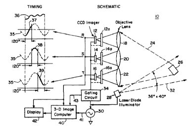
Fig. 1 is a schematic view of a three-dimensional imaging
system according to this invention including timing diagrams
for gating the CCD imagers;
Fig. 2A is a schematic view of the optical head of the
system of Fig. 1;
Fig. 2B is a cross-sectional view of an alternative
optical head for the system of Fig. 1;
Fig. 2C is a cross-sectional view of an alternative
optical head for the system of Fig. l;
Fig. 3 is a plot of illumination transmitted from and
received by the system of Fig. 1;
Fig. 4 is a side elevational view of illumination
transmitted to and reflected from the surface of an object to
be imaged according to this invention;
Fig. 5 is a detailed schematic block dlagram of the
sys~em shown in Fig. 1;
Fig. 6 is a flow chart depicting the operation of the
CA 02243494 1998-07-16
W O 97/26761 PCTrUS97100237
absolute distance conversion circuit of F-g. 5i
Fig. 7 is a three-dimensional display of an object
according to this invention;
Fig. 8 is a schematic block diagram of one of the three
synchronously gated CCD imagers of Fig. l;
Fig. 9 is a schematic block diagram of the synchronously
gated CCD imager of Fig. 2C.
There is shown in Fig. 1 improved three-dimensional
imaging system 10 which
includes three identical CCD imagers 12, 14 and 16. Objective
lenses 18, 20 and 22 receive and focus onto CCD imagers 12, 14
and 16 illumination 24 reflected from the surface of object 26
to be imaged. Illumination 24 reflected from object 26
emanates from illumination source 28 which may be a laser
diode illuminator, such as an LDP4500C laser diode, a diode
pumped solid state laser illuminator or a light emitting diode
(LE~), sinusoidally modulated at high frequency, for example,
1 MHz by sine wave generator 30 to emit illumination beam 32
to fill the imager(s) field(s) of view. An illumination
emission wavelength of 808 nm is typically used as it is near
the peak response of CCD imagers 12, 14, and 16. Although
only one object to be imaged is shown, this is not a necessary
limitation of this invention as any number of objects within
the field of view o~ system 10 are capable of belng imaged
providing the number of CCD pixels is sufficient to resolve
them.
Gating circuit 34 driven by sine wave generator 30
shutters the input of illumination 24 to each of the CCD
imagers such that each imager is turned on during a different
portion of each cycle of sinusoidally modulated illumination
~eam 32, as described in detail below with regard to Fig. 8.
CCD imagers 12, 14 and 16 may alternatively be gated by
positioning optical shutters 12a, 14a and 16a in front of the
CCD imagers. The optical shutters may be implemented with,
for example, gated microchannel plate imagers, gated proximity
focused image intensifiers, electronically switched Pockel~s
cells, liquid crystal shutters or mechanical shutters.
CA 02243494 1998-07-16
W O 97/26761 PCTrUS97/00237
Circuit 34 gates CCD imagers 12, 14 and 16 in synchronism
with the modulation frequency 35 of transmitted illumlnation
32 such that each imager is turned on or is opened during a
different portion of each full cycle 36 and off or closed
during the remainder of each cycle. In this example CCD
imagers 12, 14 and 16 are turned on for 120~ (or less)
portions 37, 38 and 39, respectively, of each cycle 36 of sine
wave 35 and off for the remainder of each cycle a significant
number of times, e.g. up to approximately 33,000 times for 1
MHz modulation frequency, per each CCD image frame time of
1/30 second. At the end of each image frame time the average
intensity levels IR~ IS and IT from each CCD pixel are read out
of the CCD imagers and provided to display 42. The intensity
levels of the corresponding pixels from each of the three CCD
imagers (i.e. pixel (1, 1) from each CCD imager) are summed
and an average pixel intensity level or a reflectance level R~
for each pixel, where I and J correspond to the X and Y pixel
locations, can be provided to display 42 for display of the
two dimensional reflectance image of object 26. The intensity
levels IR/ IS and IT could alternatively be used for other
various external applications.
Also at the end of each image frame time the intensity
levels from each pixel of CCD imagers 12, 14 and 16, IR~ I5 and
IT~ respectively, are provided to three-dimensional image
computer 40 which determines the phase angle between
transmitted illumination 32 and illumination 24 received at
each pixel. From the phase angle, the distance along the
optical axis from system 10 to each resolved element of object
26 (i.e. each element of the object imaged by a pixel) is
computed. It should be noted that, for example, pixel (1,1)
of each CCD imager resolves the same element of object 26,
thus only a single distance is computed from pixel (1,1) to an
element on object 26 using intensity information from pixels
(1,1) of each imager. If the distance from system 10 to
object 26 exceeds one half wavelength of the modulation
fre~uency then the distances from system 10 to each resolved
element on object 26 are only relative modulo A/2 distances.
CA 02243494 1998-07-16
W O 97/26761 PCT~US97/00237
In other words, this information reveals only the position of
each resolved element relative to other resolvea elements with
respect to system 10. This relative distance information is
provided at the end of every image frame time to display 42.
The absolute distance from system 10 to each image element of
object 26 resolved can also be calculated by three-dimensional
image computer 40 and provided to display 42. The third
dimension of the image (either relative or absolute) can be
combined with the two-dimensional reflectance image to form a
three-dimensional image which is displayed on display 42, e.g.
as an isometric display.
One method used to determine the absolute distance from
system 10 to each resolved element of object 26 requires the
temporary adjustment of the modulation frequency which is
accomplished by providing an adjustment signal over line 41 to
sine wave generator 30. This process is described in detail
below with regard to Fig. 6.
Three-dimensional image computer 40 also compensates for
Doppler effects due to relative movement of system 10 and
object 26 by adjusting the frequency of the on and off gating
signals to CCD imagers 12, 14 and 16 relative to the source
modulation frequency. This process, described in detail below
with regard to Fig. 5, is accomplished by providing an
adjustment signal over line 43 to gating circuit 34.
- Optical head 44, Fig. 2A, is typically configured with
objective lenses 18, 20 and 22 co-aligned and with
illumination source 28 approximately centered about the
lenses. Optical head 44 is configured such that the
corresponding pixels of each CCD imager receive reflected
illumination 24 from the same element of object 26 and thus
each resolve the same element of object 26.
Alternative optical head 44a, Fig. 2B, has only a single
objective lens 45 which receives incoming reflected
illumination 24. One third of reflected illumination 24
passes through partially transmissive mirror 46 as indicated
at 24 r and is focussed on CCD imager 12, while the remaining
two thirds of the incoming illumination 24 is reflected off
CA 02243494 1998-07-16
W O 97/26761 PCTAUS97/00237
the surface of mirror 46 and is directed to partially
transmissive mlrror 48 as indicated at 24'~. Mirror 48 passes
one half of the remaining illumination (24''') to CCD imager
14 and the other half of the illumination (24'''') is
reflected onto the surface of CCD imager 16. Although not
visible in this figure, illumination source 28 is located
proximate objective lens 45. Each corresponding pixel of the
CCD imagers 12, 14 and 16 also each receive the same reflected
illumination 24 from object 26 and thus each resolves the same
element of object 26.
Fig. 2C shows a configuration using a single CCD imager
12' and objective lens 12a' capable of simultaneously gating
and integrating the three samples per cycle of the modulated
radiation. Imagers having this capability are being
fabricated by D. Gardner of SMD, Inc., Colorado Springs,
Colorado and are described in the article by T. Spirig, P.
Seitz, O. Vietze, and F. Heitzger, "The Lock-In CCD - Two-
Dimensional Synchronous Detection of Light" IEEE ~ournal of
Quantum E7ectronics, Vol. 31, No. 9, September 1995
incorporated herein in its entirety by reference. Gating
circuit 34, Fig. 1, provides the gating signals to CCD imager
12' to synchronously gate imager 12' to obtain at least three
samples per cycle, as described below with regard to Fig. 9.
Transmitted illumination 32, Fig. 3, is modulated at an
intensity level Iv about a mean DC level IDC at a modulation
frequency of, for example, lMHz. The reflected or back
scattered illumination 24a received, for example, by one pixel
of CCD imagers 12, 14 and 16 is shown to be shifted in phase
by an angle ~. This phase shift can be used to compute the
distance of the element of object 26, Fig. 1, resolved by that
one pixel with respect to system 10. By determining the phase
shift of reflected light received by the other pixels, the
relative offset distances among the elements with respect to
system 10 can be calculated. Absolute distances of the
resolved elements of object 26 to system 10 can also be
determined.
In order to determine the phase angle difference, ~,
CA 02243494 1998-07-16
WO97126761 PCT~S97/00237
11
between the transmitted and received illumination irrespective
of the mean DC level IDC and the modulation intensity level Iv,
which will be attenuated as the illumination is propagated to
and reflected off the object 26, intensity levels of received
illumination 24 must be monitored during at least three
portions of each cycle of the modulation frequency of
transmitted illumination 32 over each image frame time either
by using at least three CCD imagers or by using a single CCD
imager which is capable of gating and integrating at least
three samples per cycle of the modulated radiation. At the
end of each image frame time the intensity levels of
illumination accumulated over the frame time during the three
portions of each cycle are used, as descrlbed below, to
calculate the phase angle of the illumination received at each
pixel location.
In synchronism with the modulation frequency of
transmitted illumination 32, from 0~ to an angle up to a
maximum of 120~, CCD imager 12 is gated on and is receiving
reflected illumination 24a while CCD imagers 14 and 16 are
gated off, thus preventing their reception of reflected
illumination 24a during this time period. At 120~, CCD ima~er
14 is gated on for the same sample period and is receiving
reflected illumination 24a while CCD imagers 12 and 16 are
gated off, thus preventing their reception of reflected
illumination during this period. At 240~, CCD imager 16 is
gated on for the same sample period and is receiving reflected
illumination 24a while CCD imagers 12 and 14 are gated off,
thus preventing their reception of reflected illumination
during this period. This completes one full cycle of
receiving illumination 24a in synchronism with the modulation
fre~uency of transmitted illumination 32. While different
gating periods may be used, the optimum gating time is 1/6 of
each cycle or 60~ for each CCD imager to be gated on. To
uniquely define the modulation phase angle three samples per
cycle are required. Optimum spacing between the samples is
120~.
This process continues until the end of each image frame
CA 02243494 1998-07-16
W O g7/26761 PCTrUS97/00237
12
time when signals IRI IS and IT for each pixel corresponding to
the received illumination 24 accumulated ir. each pixel of the
CCD imagers are provlded to three-dimensional image computer
40 where the phase angle difference ~ at each pixel (I, J) is
determined. From the computed phase angles ~1~ at each pixel
(I, J) the ranges or distances z~ between system 10 and each
resolved element of object 26 can be calculated. If system 10
is located more than one half wavelength from object 26, the
calculated distances zlJ are relative modulo A/2 offset
distances and not absolute distances. That is, these
distances indicate that, for example, one resolved element of
object 26 is 10 cm closer to system 10 than another resolved
element, rather than indicating that the one element of object
26 is 200 meters from system 10 and the other element is 200.1
meters from system 10.
The phase angle of the transmitted illumination 32 is
typically set at 0 radians, therefore, the calculated phase
angle ~RCV Of received illumination 24, Fig. 1, at each pixel
location can be used to calculate distance z of each resolved
element (i.e. the element on object 26 resolved by a given
pixel location) to system 10 according to the foilowing
formula:
2z=(c/fm)(~R~/2~) (1)
where c is the speed of light, fm is the modulation frequency
of the transmitted illumination and ~RCV iS the phase angle in
radians of the received illumination reflected from a resolved
element of object 26.
The determination of the distances Zl3 from discrete
elements of an object to system 10 is illustrated with regard
to surface 50, Fig. 4, which is positioned an unknown distance
from system 10 greater than the distance of one half
wavelength of the modulation frequency. Thus, by calculating
z according to formula (1) for each resolved element only the
relative modulo A/2 distance from an arbitrary plane 52 in
space located at a distance equal to one half of the
CA 02243494 1998-07-16
W O 97/26761 PCTAUS97100237
13
modulation frequency wavelength can be determined. Element 54
on surface 50 receives transmitted illumination 55 and
reflects illumination 56 which is received and resolved, for
example, by pixel (I, 1) of system 10. System 10 calculates
the phase angle ~RCVII of the light received by the pixel to be
0 radians. Element 58 on surface 50 is located closer to
system 10 than element 54, thus when transmitted radiation 59
impinges upon element 58 it reflects illumination 60 which
when received and resolved, for example, by pixel (I, 2) of
system 10 with a phase angle ~RCVI~ equal to 3~/2 radians.
Element 62 on surface 50 is even closer to system 10 than
element 58 and it receives transmitted illumination 63 and
reflects illumination 64 which is received and resolved, for
example, by pixel (I, 3) of system 10 with a phase angle ~RCV13
of ~ radians. Element 66 on surface 50, the closest point to
system 10, receives transmitted illumination 67 and reflects
illumination 68 which is received and resolved by, for
example, pixel (I, 4) with a phase angle ~RCV14 of ~/2 radians.
Distances z~- Z~4 can be calculated by inserting phase angles
~RCVII - ~RCV14 into equation (1). Since distance Z4 for Element
66 is the smallest, it is the closest to object 26 and is
designated as the reference point. All distances with larger
values are further from object 26. For example distances Z~4 -
z" may be calculated to be 2, 4, 6 and 8 cm, respectively.
Thus, element 66 may be designated as the zero point with the
other elements 2, 4 and 6 cm further away from system 10 than
element Z14 ~
System 10, shown in detail in Fig. 5, includes three
phase clock 70 within gating circuit 34 which is
interconnected with CCD imagers 12, 14 and 16 to turn these
imagers on at 0~, 120~ and 240~, respectively, of the
modulation frequency of transmitted illumination 32 to collect
illumination 24 reflected from object 26. Three phase clock
70 is driven by digitally controlled phase shifter 72, the
operation of which is described below, and external clock 74
whose input is a sine wave reference signal from source 30
CA 02243494 1998-07-16
WO97/26761 PCT~$971~237
14
which modulates transmitted illumination 32 from illumination
source 28. While these imagers are off, they are receiving
reflected illumination 24 but are prevented from collecting
photoelectrons. At the end of each image frame time,
typically 1/30 second, each imager 12, 14 and 16 outputs
intensity signals IR~ IS~ and IT for each pixel which
corresponds to the amount of illumination received by each
pixel of each imager during their "on" times. Amplifier 76
sums the three signals and provides a reflectance image, Rl~,
for each pixel over line 77 to display 42 or for other usage.
The intensity signals IR~ I5 and IT for each pixel are
converted to digital values by analog to digital converters
78a-c, respectively, and the digital values are provided over
lines 79, 80 and 81 to phase angle computer 82 which
calculates the phase angle of illumination received at each
pixel of the CCD imagers as follows. The process of gating
the imagers during three portions of each cycle of transmitted
illumination 32 namely, 0~, 120~ and 240~, produces three DC-
baseband images of the form:
IR= IDC+ IVCOS t '1~ +~Po )
s=IDc+I&os (~0 +2 3 ), and ( 2 )
I~=IDC+IVC05(~+~o+4 3 ),
where the bars above I~, Is~ and IT denote time averages within
an image frame time (1/30 second) and ~0 is the reference phase
value. Assuming the three CCD imagers 12, 14 and 16 have
equal gain or responsivity, or have been adjusted to be so,
then the IDC and Iv terms in each equation are identical. With
the three equations, ~, on a pixel by pixel basis can be
solved by taking the three pixel stream intensity values IR~ I~
and IT from each imager 12, 14 and 16 supplied over lines 7~,
80 and 81 to phase angle computer 82 within three-dimensional
image computer 40. Within phase angle computer 82 in-phase
and quadrature conversion computation is performed by in-phase
and quadrature conversion circuit 84 such as a digital signal
processor or the equivalent which condenses the three phases
CA 02243494 1998-07-16
WO97/26761 PCT~S97/00237
down to two phase values 90~ apart. Digi~lzed n-phase signal
(I) which is equal to
I =~V COS ('~4+f~)o) (3)
is supplied over line 85 to cartesian-to-polar coordinate
transformation circuit 86 such as a Raytheon TMC 2330 or any
other high speed phase processor on a pixel by pixel basis.
Digitized quadrature signal (Q) equal to
P = IV SIN (~+~o) (4)
is supplied over line 87 also to cartesian-to-polar coordinate
conversion circuit 86 on a pixel by pixel basis. The phase
angle, ~IJ =tan~' I/Q, is solved for each pixel of the CCD image
in circuit 86. Using equation (l) above and the determined
phase angle ~ for each pixel, the relative off set distance
of each element of an object resolved by the CCD imagers is
calculated in relative offset range circuit 88 which may be a
digital signal processor that performs a relative offset range
algorithm. The relative offset distances of each pixel
location/resolved element are supplied to display 42. The
relative range information from relative offset range
conversion circuit 88 can be used to display a three-
dimensional image on display 42. Three-dimensional imaging
displays are commercially available from, for example,
NuVision, (SGS60 Stereotek), and Dimension Technologies, Inc.,
(DTIllOOC). The acquired 3-dimensional image data need not be
provided to a visual display. This data can be directly
provided to any system requiring high speed, three dimensional
image data.
Phase angle signals ~1, are also processed by an absolute
distance conversion circuit 90 such as a digital signal
processor that performs an absolute distance conversion
algorithm which determines the absolute distance of each
resolved point from system lO and supplies that information to
display 42 to display a three-dimensional image of the object
including the absolute range of the object from system lO.
Both the phase angle and ranging computations are
CA 02243494 l998-07-l6
W 0 97/26761 PCTAUS97/00237
16
performed during the periods between CCD image collection
frames when the image intensity data is being read OUt of the
imagers. Accordingly system lO provides real-time three-
dimensional imaging.
Doppler compensation loop 92 is used to introduce a
Doppler frequency shift when imaging system 10 is, for
example, mounted on a moving platform, such as a helicopter,
and is imaging a stationary object or if the object is moving
and system 10 is stationary. Adder 94 receives n number of
phase angles over a time period t and outputs an average phase
angle to phase change determination circuit 96 which outputs
over line g7 a signal, d~/dt. This signal indicates the time
averaged rate of change of the phase angle between, for
example, time tl and time to due to the Doppler effect which
occurs because the object being imaged is moving relative to
system 10. The d~/dt signal from line 97 is subtracted from a
phase angle reference signal and the phase difference signal
is supplied over line 43 to digitally controlled phase shifter
72 such as a digital signal processor within gating circuit 34
which alters the timing of the three phase clock signals in
clock 70 to increase or decrease, as necessary, the frequency
of the clock signals until, for example, ~(tl)is equal to
~(to)and d~/dt is equal to zero.
For example, if system 10 and the object being imaged are
moving relative to each other at a speed of 10 meters per
second, d~/dt is equal to 10 radians per second or 1.6Hz.
Thus, to compensate for Doppler effects the frequency of the
three phase clock signals in clock 70 is increased from, for
example, 1,000,000 Hz to 1,000,001.6 Hz which causes d~/dt to
be equal to 0.
As noted above, if system 10 is more than one wavelength
away from the object being imaged the distances zl~ computed
for each resolved element of the object are only relative
modulo ~/2 distances. With the typical lMHz modulation
frequency the measurement range is 150 meters. In other
CA 02243494 1998-07-16
W O 97/26761 PCT~US97/00237
17
words, as long as the object being imaged is within 150 meters
of system 10, the calculated distances zl~ are the absolute
distances of each resolved element from system 10. However,
if the object is greater than 150 meters from system 10, the
distances z" are only relative modulo A/2 distances.
Absolute distance conversion circuit 90, which operates
according to flow chart 100, Fig. 6, is used to determine the
absolute range of each resolved point on the imaged obiect to
system 10. Circuit 90 calculates the phase angles ~ for each
pixel at the initial modulation frequency, f" in step 102. At
step 104 the absolute distance conversion circuit 90, Fig. 5,
by a signal over line 97, changes by a predetermined increment
the modulation fre~uency of illumination source 28 by
adjusting the output of sine wave generator 30 to f2. At step
106 the phase angles ~2 at the reduced modulation frequency,
f~, are calculated for each pixel. At step 108 the absolute
range ZABS for each pixel is calculated according to the
following equation:
ZA~S= ( 4C ~ ( ddp ) (5)
where c is the speed of light, d~ equals ~2 - ~ and df equals
f2-f,. The absolute distance determination function of
absolute distance conversion circuit 90 may be accomplished by
other known techniques.
Display 120, Fig. 7, is a typical three-dimensional
display of object 122 which may be generated using system 10
according to this invention. In this display the absolute
distance of each resolved element of object 22 is displayed on
the Z axis. This display could also be a display of the
relative offset distance of each resolved element of object
122.
In order to accomplish the high speed shuttering
necessary for three-dimensional imaging according to this
invention, CCD imagers 12, 14 and 16 are configured to operate
as synchronously gated high speed CCD imagers. The imagers'
configuration is only depicted with regard to CCD imager 12,
CA 02243494 1998-07-16
W O 97/26761 PCTrUS97/00237
18
Fig. 8, as imagers 14 and 16 are identically configured.
CCD imager 12 includes a plurality of columns of
photosensitive areas only two of which, 130 and 132, are
shown. Each column incudes a plurality of pixels 130a-b and
132a-b. Although for clarity sake an array of only two
columns with two pixels in each column is shown, a typical CCD
imager for use in this invention would include, for example,
an array of 512 columns with 512 pixels in each column. Each
pixel includes a photosensitive area, such as areas 134a-b and
136a-b. Above each photosensitive area is included a
microlens, such as lenses 138a-b and 140a-b, which increases
the effective photosensitive area of each pixel to typically
80%. Photons incident upon CCD imager 12 from illumination
24, Fig. 1, reflected from object 26 generate photoelectrons
which are collected or integrated by photosites 134a-b and
136a-b. The photoelectrons collected at the photosites are
then selectively routed by means of switches 142a-b and 144a-b
to either storage wells 146a-b and 148a-b, respectively, or to
photoelectron drains 150a-b and 1~2a-b, respectively.
Switches 142a-b and 144a-b are operated by a control signal
from vertical shift registers 154 and 156 originating from
gating circuit 34.
CCD imager 12, as with conventional CCD imagers, has a
1/30 second image frame time. However, as noted above, system
10, Fig. 1, requires the illumination input to CCD imager 12
(and CCD imagers 14 and 16) be gated many times during each
image frame time. That is, system 10 requires that CCD imager
12 be turned on (to collect photoelectrons from reflected
illumination 24) and off (to prevent collection of
photoelectrons from reflected illumination 24) many times
during each 1/30 second image frame time. Thus, when CCD
imager 12 is to be gated on to collect photoelectrons from
reflected illumination 24 once each cycle of sinusoidally
modulated illumination beam 32 then gating circuit 34, through
vertical shift registers 154 and 156, interconnects photosites
134a-b and 136a-b to storage wells 146a-b and 148a-b so that
the photoelectrons are collected and stored in the storage
CA 02243494 1998-07-16
wO97n6761 PCT~S97/00237
wells. And, during the remainder of each cycle, gating
circuit 34, through vertical shift registers 154 and 156,
interconnects the photosites with photoelectron drains 150a-b
and 152a-b so that the photoelectrons from the photosites are
removed or drained away and prevented from ~eing collected in
the storage wells. In this switch position CCD imager 12 is
gated off and the "shutter" to CCD imager 12 is effectively
closed. When the switch is in the other position and the
photoelectrons from the photosites are routed to the storage
wells the ~shutter" to CCD imager 12 is effectively opened.
In the example of Fig. 1, CCD imager 12 s gated on
(shutter open) from 0~ to 120~ of each cycle of the modulation
frequency of transmitted illumination 32 and gated off
(shutter closed) for the remainder of the cycle. When any one
CCD imager is gated on by gating circuit 34, the other two CCD
imagers are simultaneously gated off. The electronlc
shuttering or gating can operate at rates up to approximately
3MHz. Accordingly, the CCD imagers 12, 14 and 16 can each be
gated on and off to obtain as many as approximately 33,000
samples for each imager during each 1/30 second image frame
time which are accumulated in the storage wells.
At the end of each 1/30 second frame time all of the
photoelectrons which were accumulated over the image frame
time in storage wells 146a-b and 148a-b are shifted down
storage well columns 158 and 160 by means of vertical shift
registers 154 and 156, respectively. Vertical shift registers
154 and 156 shift the contents of the storage wells to
horizontal shift registers 162 and 164 which then output
through amplifier 166, pixel by pixel, serial reflectance
image IR. The output from CCD imager 12 is supplied to both
amplifier 76 and phase angle computer 82 (Fig. 5) where, in
conjunction with the outputs from imagers 14 and 16, it is
used to display the two-dimensional reflectance image on
display 42 and to calculate the phase angle of illumination 24
reflected from object 26 to each pixel of the CCD imagers 12,
14 and 16.
CCD imagers 12, 14 and 16 may be gated by other means
CA 02243494 1998-07-16
W O 97/26761 PCTAUS97100237
which may be apparent to those skilled in the art as long as
the gating means are capable of turning each CCD imager on and
off with sufficiently high frequency. The hlgher the
frequency for gating the CCD imagers the lower are the minimum
detectable range differences. Three-dimensional lmagers with
shorter minimum resolvable range have greater applicability.
Alternatively, if a single CCD imager, such as CCD imager
12', Fig. 2C, is used it is configured as shown in Fig. 9. In
this embodiment each photosite is selectively interconnected
with three storage wells. Photosites 134a' and 134b' are
selectively interconnected with storage wells 146a'(R),
146a''(S), 146a'''(T), and 146b'(R) 146b''(S), 146bb'''(T),
respectively. Photosites 136a' and 136b' are selectively
interconnected with storage wells 148a'(R), 148a''(S),
148a'''(T) and 148b'(R), 148b''(S), 146b'''(T), respectively.
Under the control of gating circuit 34, through vertical
shift register 154', gating signals are provided to switches
142a'-b', and 144a'-b' which selectively route photoelectrons
from the photosites to the appropriate one of the three
storage wells (R, S and T) during the correct portion of each
cycle of sinusoidally modulated illumination beam 32. That
is, during the first 1/3 cycle, for example, of each cycle of
sinusoidally modulated illumination beam 32, photoelectrons
collected in the photosites are pro~ided to storage well R for
each pixel location. During the next 1/3 cycle, gating
circuit 34, through vertical shift register 154', provides a
signal to each switch to interconnect the photosites with
storage wells S so that these storage wells collect
photoelectrons during that 1/3 portion of the cycle. And,
during the final 1/3 cycle, gating circuit 34 interconnects
the photosites with the T storage wells so that they collect
photoelectrons during that portion of the cycle. At the end
of the 1/30 second image frame time after which each storage
well R,S, and T of each pixel has cumulatively collected
photoelectrons during a large number of cycles, the
photoelectrons from the storage wells are transferred to the
corresponding vertlcal shift register columns 158' and 160'
CA 02243494 1998-07-16
W O 97t26761 PCTAUS97100237
21
under the control of vertical shift reglsters 154' and 156'.
Vertical shift registers 154' and 156' then shift the
photoelectrons to horizontal shift registers 162' and 164'
which serially output through amplifier 166', on a pixel by
pixel, basis the three intensity s~gnals IRI IS and IT. These
intensity signals IR~ IS and IT for each pixel are provided to
amplifier 76 and lines 79, 80 and 81, Fig. 5. Since these
signals are output serially instead of in parallel as in Fig.
5, any appropriate manipulation to provide a parallel input to
amplifier 76, and lines 79, 80 and 81 may be used, which will
be apparent to those skilled in the art.
Although specific features of this invention are shown in
some drawings and not others, this is for convenience only as
each feature may be combined with any or all of the other
features in accordance with the invention.
Other embodiments will occur to those skilled in the art
and are within the following claims:
What is claimed is: