Note: Descriptions are shown in the official language in which they were submitted.
~ CA 02243506 l998-07-l6
W O 97/313~36 PCT~US97/00850 - -
~JLTIPLE I~rTEEUFACE INPlrT/OU-l~Ul PORT
FOR A PERIP ~ ~AT~ DE~VICE
RA~R~UnDD
Field of the Invention
5The present invention relates generally to data
communications between a host computer and a peripheral
device, and more particularly, to a multiple interface
input/output port that enables a peripheral device to be
connected to any one of a plurality of different types of
interface buses of a host computer.
Description of the Prior Art
A variety of so-called interface buses exist for
enabling communication between a host computer and one or
more peripheral devices, such as disk drives, printers,
scanners, modems and the like. These interface buses include
the Small Computer Systems Interface (SCSI) bus, which has
several versions (i.e., SCSI-1, SCSI-2 and SCSI-3), and a
number of parallel port buses, including the standard uni-
directional parallel port found in early IBM PCs, the bi-
20 directional parallel port found in IBM PS-2s, the extended
capability port (ECP), the enhanced parallel port (EPP), and
the IEEE-1284 standard parallel port. A host computer might
have o:ne or more of these interface buses, or 1'ports", to
which ~eripheral devices can be connected. In other cases,
the host computer may only have a single interface port for
connecting peripheral devices. Communication of data over
each of these different interface buses is usually performed
CA 02243~06 1998-07-16
W O 97/31386 PCT~US97/00850 -
in accordance with a communications protocol specific to the
particular bus 6tructure.
Unfortunately, the existence of such a variety of
interface buses and associated communication protocols
creates compatibility problems and generally makes the
purchase of peripheral equipment more difficult and confusing
for a typical consumer. For example, a consumer may purchase
a new disk drive that is configured to communicate across a
SCSI-2 interface, only to find that the computer to which the
10 disk drive is to be attached only has a single, parallel port
interface. In an attempt to provide a solution to this
problem, a number of vendors provide parallel port-to-SCSI
translators that can be connected between a SCSI peripheral
and the parallel port of a personal computer for enabling
communication of SCSI comm~n~R to the peripheral device via
the host parallel port interface. While such an adapter
provides a solution to the incompatibility problem, the
consumer is faced with the cost of an additional component,
as well as the time and effort needed to connect the adapter
and install any necessary driver software.
Farago, U.S. Patent No. 4,972,470, describes a
"programmable connector" for a host computer that can be
programmed to reconfigure its physical connections to match
the serial inter~ace characteristics, e.g., RS-232, RS-422 or
25 RS-485, of a peripheral device to which it is connected. For
example, the connector of Farago allows the user to
reconfigure the I/O interface of the host computer so that it
matches the I/O interface of a particular peripheral device
that the user wishes to connect. While this may eliminate
30 the need to purchase a different interface adapter for each
new application, the programmable connector of Farago
requires the user to identify the serial interface protocol,
e.g., RS-232, RS-422 or RS-485, of the peripheral device, and
then to download the appropriate programming instructions to
the programmable connector in order to reconfigure the
physical interface of the connector to match that of the
peripheral interface. Unskilled users may find such
CA 02243~06 1998-07-16
WO 971313~86 PCT~US97/00850 -
progr~mming difficult and con~using. Finally, because the
connector of Farago simply reconfigures the necessary timing,
pin-olts, voltages and other physical parameters to match the
physical inter~ace characteristics of the device to which it
is connected, it does not provide any sort of logical
protocol translation necessary to enable communication
between interfaces that operate in accordance with more
sophi~3ticated interface protocols, such as a SCSI protocol or
the more advanced parallel port protocols.
~atif et al., U.S. Patent No. 5,289,580, discloses
an input/output controller that can be programmed to interact
with a variety of interface protocols, such as IPI, SCSI and
Messa~e Level Interface (M~I). While the input/output
controller provides the necessary logical protocol
trans]ation for enabling communication between two inter~ace
buses that communicate in accordance with different interface
protocols, it too must be "programmed~ to provide the
appropriate protocol translation and does not automatically
detect the type of interface bus to which it is connected.
Consec~uently, the input/output controller of Latif et al.
re~uires signi~icant knowledge and input on the part of the
user.
Accordingly, there is a need for a multiple
interface input/output port adapted for use in a peripheral
25 device that is capable of automatically detecting the type of
interface bus to which it is connected in a host computer and
then routing communications between the two devices through
an appropriate interface adapter, if necessary, in a manner
transparent to the user. Such apparatus would eliminate the
30 need for cumbersome adapter devices and would provide a more
user-friendly operation. The present invention satisfies
this need.
.
SUMMARY OF THE LNV~NllON
- The present invention is directed to a multiple
3~ interface input/output port for a peripheral device that is
capable of automatically detecting the type of interface bus
-
CA 02243~06 l998-07-l6
W O 97/31386 PCTrUS97/00850 -
to which it is connected in a host computer and then routing
communications between the two devices through an appropriate
interface adapter, if necessary, in a manner transparent to
the user. According to the present invention, the multiple
interface input/output port comprises a connector, and an
interface bus detection circuit electrically coupled to the
connector. The interface bus detection circuit automatically
detects the type (e.g., SCSI, parallel port, etc.) of the
interface bus to which the connector is connected. The
10 multiple interface input/output port further comprises a
plurality of interface adapters, each connected between the
connector and an internal interface bus of the peripheral
device. Each of the interface adapters is capable of
providing the necessary physical and logical translation
15 between the interface bus of the peripheral device and a
respective one of the plurality of different types of
interfaces buses to which the peripheral device may be
connected on a host computer. Once the type of the inter~ace
bus of the host computer has been detected by the interface
20 bus detection circuit, an appropriate one of the interface
adapters is enabled to provide the necessary translation
between the detected interface bus of the host computer and
the internal interface bus of the peripheral device.
Communications between the host computer and the peripheral
25 device are then routed through that interface adapter.
According to yet another aspect o~ the present
invention, the multiple interface input/output port further
comprises a pass-through bus for enabling communication
between a third device and the host computer through the
30 peripheral device.
In a preferred embodiment of the present invention,
the peripheral device has a Small Computer Systems Interface
(SCSI) bus for communicating with a host computer, and the
multiple interface input/output port of the present invention
allows the peripheral device to communicate with either a
SCSI inter~ace or a parallel port interface on the host
computer. In accordance with this embodiment, the interface
CA 02243~06 1998-07-16
W O 97/31386 PCTGUS97~0850 -
bus detection circuit detects whether the interface bus of
the host computer is a SCSI bus or a parallel port interface
bus. When a parallel port interface is detected,
commw1ications between the host computer and peripheral
5 device are routed through a Parallel Port-to-SCSI (PP-SCSI)
interl~ace adapter that provides the necessary translation
between the parallel port of the host computer and the S~SI
bus of the peripheral device. When the inter~ace bus
detect:ion circuit detects that the peripheral device is
10 connected to a SCSI bus on the host computer, communications
are routed through a repeater circuit that redrives signals
trans~itted between the SCSI bus of the peripheral device and
the SCSI bus of the host computer.
According to another aspect o~ the present
invent:ion, the interface bus detection circuit comprises
means for comparing signal levels on selected ones of the
lines of an interface bus under consideration to a reference
potent:ial to determine which of the selected lines is
grounded. The interface bus type is then indicated based on
20 the determination of which of its lines are grounded. In a
preferred embodiment of the interface bus detection circuit,
the ci.rcuit is capable of detecting whether an interface bus
is a ',CSI bus or a peripheral bus. In this embodiment, the
circuit comprises means for comparing voltage levels on each
25 of lines 14, 16, 19 and 25 of an interface bus to a reference
potential to determine which of these lines are grounded. A
SCSI bus is detected when lines 14 and 16 are determined to
be grounded; a parallel port interface is detected when
either (i) line 25 of the interface bus under consideration
is determined to be grounded or (ii) line 19 is determined to
be grGunded, and at least one of lines 14 and 16 are
determined not to be grounded.
An alternative embodiment of the interface bus
detection circuit detects whether line 25 of an interface bus
35 under consideration is grounded. The circuit identifies the
interface bus as a SCSI bus when line 25 is not grounded, and
~ CA 02243~06 1998-07-16
W O 97131386 PCTAUS97/00850 - -
identifies the interface bus as a parallel port interface
when line 25 is grounded.
Additional features and advantages of the present
invention will become evident hereinafter.
BRIEF DESCRIPTION OF ~HB DRAWINGS
The foregoing summary, as well as the following
detailed description of the preferred embodiments, is better
understood when read in conjunction with the appended
drawings. For the purpose of illustrating the invention,
there is shown in the drawings embodiments that are presently
preferred, it being understood, however, that the invention
is not limited to the specific methods and instrumentalities
disclosed. In the drawings:
Figure 1 is a block diagram o~ a multiple-lnterface
input/output port according to the present invention;
Figure 2 is a block diagram of a preferred
embodiment of a multiple-interface input/output port
according to the present invention that enables a peripheral
device to communicate with either a SCSI interface or a
20 parallel port interface on a host computer;
Figure 3 i9 a block diagram illustrating :Eurther
details of the interface bus detection and control block of
Figure 2;
Figure 4 is a schematic diagram illustrating
further details of the Host I/O Control block of Figure 2;
Figure 5 is a schematic diagram illustrating
further details of the Pass-through I/O Control block of
Figure 2;
Figure 6 is a schematic diagram illustrating
further details of the ~evice I/O Control block of Figure 2.
Figure 7 is a state diagram illustrating a method
for determining whether an interface bus is a SCSI bus or a
parallel port interface bus in accordance with a preferred
embodiment of the present invention;
Figure 8 is a schematic diagram of one embodiment
of an interface bus detection circuit for determining whether
~ CA 02243506 1998-07-16
wo 97/313,B6 PCTrUS97/008S0 -
an interface bus is a SCSI bus or a parallel port inter~ace
bus;
Figure 9 is a schematic diagram of a second
embod-ment of an interface bus detection circuit according to
the present invention;
Figure 10 is a schematic diagram of a third
embodiment of an interface bus detection circuit according to
the present invention;
Figures ll(a) and ll(b) illustrate further details
of the parallel port-to-SCSI (PP-SCSI) interface adapter of
Figure 2; and
Figures 12(a) and 12(b) illustrate further detaila
of the SCSI-to-SCSI repeater circuit of Figure 2 in
accorcLance with a preferred embodiment of the present
invention.
~ET~TT.Rn DESCRIPTION OF THE PREFERRED EMBODIMENT
Referring to the drawings wherein like numera~s
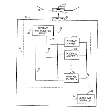
indicate like elements throughout, there is shown in Figure 1
a multiple interface input/output port 11 in accordance with
the present invention that enables communication between a
peripheral device 10 having one type of interface bus 14 and
a host computer 16 having any one of a plurality of different
types of interface buses, e.g., interface bus 18. For
example, the inter~ace bus 14 of the peripheral device 10 may
25 be a Small Computer Systems Interface (SCSI) bus, such as a
SCSI-1, SCSI-2 or SCSI-3 bus. The interface bus 18 of the
host computer 16 might be one of the different types of SCSI
buses, or one of the various types of parallel port buses,
e.g., ECP, EPP or IEEE-1284. The multiple interface
input/output port 11 of the present invention automatically
detects the type of host computer interface bus to which it
is connected and then routes communications between the two
devices through an appropriate interface adapter, if
necessary, in a manner transparent to the user. Thus,
communication between the peripheral device and host computer
is enabled despite ~he fact that their respective interface
CA 02243~06 l998-07-l6
W O 97/31386 PCT~US97/00850 - -
buses are different. The multiple interface input/output
port 11 of the present invention may be employed in a wide
variety of different peripheral devices, such as disk drives,
printers, CD-ROM drives and the like.
As shown in Figure 1, the multiple interface
input/output port 11 of the present invention comprises a
connector 20 adapted to connect to a particular interf~ace bus
18 of the host computer 16 via a mating connector 21 on the
host computer 16. The connectors 20, 21 can be connected
either directly, or via a suitable cable (not shown). An
interface bus detection circuit 22 iS electrically coupled to
the connector 20 via an intermediate bus 24. Upon connection
of the connector 20 to the interface bus 18 of the host
computer, which effectively makes the intermediate bus 24 an
15 extension of the interface bus 18 of the host computer 16,
the interface bus detection circuit 22 operates to detect the
type (e.g., SCSI, parallel port, etc.~ of the interface bus
18 to which it is now connected. A plurality of interi~ace
adapters 26, 28, 30 are each electrically coupled between the
connector 20 (i.e., intermediate bus 24) and the internal
interface bus 14 o~ the peripheral device 10. Each interface
adapter 2 6, 28, 30 provides the necessary physical and
logical interface protocol translation between the interface
bus 14 of the peripheral device 10 and a respective one of a
plurality of different types of interface buses to which the
peripheral device 10 may be connected on the host computer,
e.g., computer 16. In the embodiment shown, each of the
interface adapters 26, 28, 30 is coupled via a respective
line 32, 34, 36 to the interface bus detection circuit 22 ~or
receiving an enabling signal from the interface bus detection
circuit.
In accordance with the present invention, the
interface bus detection circuit 22 automatically detects the
type of interface bus to which it is connected, and then
35 enables an appropriate one of the plurality of interface
adapters 26, 28, 30 based upon the detected type (e.g., SCSI,
parallel port, etc.) of the interface bus to which it is
CA 02243~06 1998-07-16
W O 97/313'56 PCTAUS97/00850 - -
connec~ted, e.g., interface bus 18 of host computer 16. The
enabled interface adapter then provides any necessary
physical and logical protocol translation between the
interface bus 14 of the peripheral device 10 and the detected
5 type o~ interface bus to which it is conne~ted. Thus, the
I/O controller 12 of the peripheral device 10 can communicate
over its inter~ace bus 14 to the host computer 16
irresF~ective of the type of interface bus to which it is
connected on the host computer 18.
For example, assuming that the interface bus 14 o~
the peripheral device 10 is a SCSI-2 bus, and that the
inter~ace bus 18 of the host computer 16 is a parallel port
bus, one of the interface adapters 26, 28, 30 may comprise a
parallel port-to-SCSI (PP-SCSI) interface adapter. With
15 appropriate software drlvers, the SCSI I/O controller 12 of
the peripheral device 10 can transmit and receive SCSI
commands over its internal interface bus 14 in accordance
with the SCSI-2 protocol, while the PP-SCSI interface adapter
provides the necessary physical and logical protocol
translation to transmit and receive those commands to and
~rom the parallel port interface 18 of the host computer 16.
On the other hand, because the inter~ace bus 14 of the
peripheral device 10 and the interface bus 18 of the host
computer 16 may in some cases be of the same type, in which
25 case no protocol translation is really needed, one of the
interface adapters 26, 28, 30 may comprise a repeater circuit
that operates simply to redrive signals transmitted between
the interface buses 14, 18 of the peripheral device 10 and
host computer 16. The repeater circuit would be enabled
30 whenever the interface bus 14 of the peripheral device 10 is
of the same type as the detected interface bus 18 of the host
computer 16. Although not illustrated in Figure 1, the
multiple interface input/output port 11 may further comprise
means ~or routing data communicated between the interface
35 buses 14, 18 of the peripheral device 10 and host computer 16
through the particular interface adapter (or repeater
circuit) that has been enabled.
CA 02243~06 1998-07-l6
WO97/31386 PCT~S97/00850-
Most interface buses comprise a plurality of lines,
some of which may be defined to carry data or control signals
and others o~ which may carry a system ground. A particular
type of interface bus is typically characterized by
5 predetermined ones of the lines of the interface bus being
grounded. Different lines are grounded on dif~erent types of
interface buses. According to the present invention, as
described hereinafter in accordance with a preferred
embodiment thereof, the interface bus detection circuit 22
comprises means for comparing signal levels on selected ones
of the lines of the host inter~ace bus to a reference
potential to determine which of the selected lines is
grounded, and means for indicating the type of the host
interface bus based on the determination of which of its
lines are grounded.
Overview of the Preferred Embodiment
Figure 2 is a block diagram of a preferred
embodiment of a multiple interface input/output port 40 in
accordance with the present invention, which is embodied as
20 part of a peripheral device (not shown) having an internal
interface bus 60. According to the preferred embodiment, the
multiple interface input/output port 40 of the present
invention comprises a connector 42 (analogous to connector 20
of Figure 1) that i8 adapted to connect to an inter~ace bus
25 or port (not shown) on a host computer (not shown). In the
preferred embodiment, the connector 42 comprises a 25-pin DB
connector, however, in other embodiments, the connector may
comprise a 36-pin Centronics, 36-pin High Density, 50-pin
Centronics or 50-pin High Density connector. When the
connector 42 is connected to an interface bus of a host
computer, an intermediate bus 44 of the multiple interface
input/output port 40 (analogous to intermediate bus 24 of
Figure 1) serves as an extension of the host interface bus.
In the present embodiment, the internal interface
35 bus 60 of the peripheral device is a SCSI-2 bus. As
described hereina~ter, the multiple interface input/output
CA 02243~06 1998-07-16
W O 97/313,B6 PCT~US97/00850 - -
- 11 --
port 40 of the preferred embodiment is designed to enable
communication between the SCSI-2 bus 60 of the peripheral
device and either another SCSI-2 bus on the host computer, or
a difierent type of bus such as, ~or example, the standard
5 unidi~ectional or bi-directional parallel port bus, the
extencled parallel port bus (EPP) or the enhanced capability
port ~ECP).
An inter~ace bus detection and control circuit 46
is coupled to selected lines 45 of the intermediate bus 44
for automatically detecting the type of inter~ace bus to
which it is connected on the host computer. Based on this
determination, the interface bus detection and control
circuit 46 provides "mode" and "enable" signals on lines 48
for purposes described hereina~ter.
A SCSI-to-SCSI repeater clrcuit 54 and a parallel
port-to-SCSI (PP-SCSI) interface adapter 56 are each coupled
in parallel between the intermediate bus 44 and the interface
bus 60 o~ the peripheral device via respective I/0 control
blocks 50 and 58. As described hereinafter in greater
20 detail, the SCSI-to-SCSI repeater circuit 54 serves to
redrive signals transmitted between the interface bus 60 of
the peripheral device and the inter~ace bus of the host
computer when both interface buses are of the same type
(i.e., SCSI-2). The PP-SCSI interface adapter 56 provides
25 physical and logical protocol translation between the host
inter~ace bus and the inter~ace bus 60 o~ the peripheral
device when the host interface bus is of a different type
than the SCSI-2 bus 60 of the peripheral device. With
appropriate software drivers, the peripheral device can
continue to transmit and receive SCSI commands over its
interface bus 60 in accordance with the SCSI-2 protocol,
while the PP-SCSI interface adapter 56 provides the necessary
physic~l and logical protocol translation to transmit and
receive those commands to and from the detected parallel port
interface bus of the host computer via intermediate bus 44
and co:nnector 42.
CA 02243~06 l998-07-l6
W O 97/31386 PCTrUS97/008S0 - - 12 -
Once the-interface bus detection circuit 46 of the
present embodiment determines whether the connector 42 is
connected to a SCSI bus or a parallel port bus on the host
computer, the interface bus detection circuit 46 provides
"mode" and "enable" signals on lines 48 in order to enable
either the SCSI-SCSI repeater circuit 54 or the PP-SCSI
interface adapter 56, as appropriate. In the present
embodiment, a particular one of the two adapters 54, 56 is
enabled by routing communications through that adapter via
10 the Host and Device I/O control blocks 50 and 58. The Host
and Device I/O control blocks 50, 58 are controlled by the
~'mode" and "enable" signals provided on lines 48 by the
interface bus detection and control block 46. In the present
embodiment, it is primarily the "mode" signal that determines
15 whether communications are routed through the SCSI-to-SCSI
repeater circuit 54 or the PP-SCSI interface adapter 56.
As can be appreciated, in the present embodiment,
the SCSI-to-SCSI repeater circuit 54 and the PP-to-SCSI
interface adapter 56 do not themselves receive "enabling"
20 signals from the interface bus detection and control circuit
46. Rather, as described above, one of the two circuits 54,
56 is enabled by routing communications through that circuit
via the Host and Device I/O control blocks 50 and 58. Figure
1 illustrates an alternative possibility where the respective
25 interface adapters (and/or repeater circuit) 26, 28, 30
receive respective enabling signals ~rom the interface bus
detection circuit 22 via lines 32, 34 and 36. AS used herein
and in the appended claims, the terms ~'enable~' and "enabling"
are intended to encompass all such possibilities.
In the present embodiment, the connector 42
comprises a 25 pin DSUB connector having 25 pins numbered
consecutively, and the intermediate bus 44 likewise comprises
25 lines each coupled to a respective one of the pins of the
connector 42. Table 1 illustrates how the 25 pins of the
35 connector 42 and corresponding 25 lines of the intermediate
bus 44 are defined, in accordance with the present invention,
for both SCSI-2 and parallel port connections.
CA 02243506 1998-07-16
W O 97131386 PCT~US97/00850 - -
- 13 -
-
LINE #SCSI FunctionPP Function
1 R~O ~.~TROBE
2 MSG D1
3 I/O D2
4 ~.~T D3
ACK D4
6 BSY D5
7 G~OUND D6
8 DB0 D7
10 9 GROU~n D8
DB3 ~CK
11 DB5 BUSY
12 DB6 ~ROR
13 DB7 SRT~CT
1514 GROVND n~
C/P ~FAUT~T
16 GRorrNn nTr~IT
17 ATN ~.S~T.RCT I~
18 GROUND GROTn~n
2019 SEL GRor~Nn
DBP ~ouNn
21 DB1 GROTTNn
22 DB~ ~.~T~n
23 DB4 GROUND
2524 ~.'ROUNn GRoT~Nn
TERM PWR ~nuND
_able 1. S~SI and Parallel Port (P.) De~initions for Inter .ediate
Bus 44
Collectively, there are twenty-two lines (1-17 and 19-23)
30 designated to carry data and/or control signals in accordance
with either a SCSI or parallel port connection, and two lines
defined as dedicated grounds ~18 and 24). Line 25 carries
termination power when the host interface bus is a SCSI bus,
such as a SCSI-2 bus.
A data transmission cable can be employed to
connect the 25-pin DB connector 42 of the multiple interface
input/output port 40 to a corresponding connector of the
interface bus (SCSI or parallel port) of the host computer.
In the case where the mating connector on the host computer
i8 also a 25-pin DB connector (either SCSI or parallel port),
connection between-the connector 42 and the particular
CA 02243~06 l998-07-l6
WO 97/31386 P~T/US97100850
-- 14
interface port on the host computer is preferably made using
an interchangeable SCSI/Parallel Port cable, such as that
claimed and described in co-pending application Serial No.
08/439,776, filed May 12, 1995, and entitled "Combined
SCSI/Parallel Port Cable".
Referring still to Figure 2, lines 1-17 and 19-23
(twenty-two lines total) of the intermediate bus 44 are
provided to the Host I/O control block 50. The Host I/O
Control block 50 provides these lines to the SCSI-to-SCSI
repeater circuit 54 and to the PP-SCSI interface adapter 56,
respectively, via an internal HostIN bus 52. (Note: the bus
widths are indicated in Figure 2 for each bus, e.g., "22",
"18", "25" .) Lines 18 and 24 of the intermediate bus 44 are
grounded, and line 25 (not shown) is used to carry
termination power from the host computer when the interface
bus of the host computer to which the peripheral is connected
is of the same type as the internal bus 60 of the peripheral,
i.e., a SCSI-2 bus. Line 25 provides a ground when the host
interface bus of the host computer is a parallel port bus.
The interface bus 60 O~ the peripheral device
comprises eighteen signal lines that correspond to lines 1-6,
8, 10-13, 15, 17 and 19-23 of the intermediate bus 44. SCSI
signals to be transmitted from the peripheral device to the
host computer are provided by the Device I/0 Control block 5 8
25 to the SCSI-SCSI repeater circuit 54 and the PP-SCSI
interface adapter 56, via an internal DeviceIN bus 64.
As described hereinafter in greater detail, the
SCSI-to-SCSI repeater circuit 54 redrives signals received on
lines 1-6, 8, 10-13, 15, 17 and 19-23 of the HostIN bus 52
and provides these redriven signals to the Device I/O Control
block via an internal SCSI-SCSI OUT bus 62. Lines 7, 9, 14
and 16 of the HostIN bus 52 are ignored in the SCSI-SCSI
repeater circuit and are not provided to the input o~ the
Device I/0 Control block 58. Signals received by the SCSI-
35 SCSI repeater circuit 54 from the Device I/O Control block 58via the DeviceIN bus 64 are likewise redriven and provided to
an input of the Host I/O Control block 5 0 via corresponding
CA 02243~06 1998-07-16
W O 97/31386 PCTAUS97/008S0 - -
~ 15 -
lines 1-6, 8, 10-13, 15, 17 and 19-23 of a twenty-two line
internal SCSI-Host OUT bus 70. Lines 7, 9, 14 and 16 of the
SCSI-]~ost OUT bus 70 are grounded.
The PP-to-SCSI interface adapter 56 receives
signa:Ls transmitted from the host computer via the HostIN bus
52 and, when the interface bus of the host computer is a
paral:Lel port bus, provides both logical and physical
trans:Lation of signals received on the HostIN bus 52 in a
paral~el port format into appropriate SCSI-2 signals that are
then provided via an eighteen line internal PP-SCSI OUT bus
66 to an input of the Device I/O Control block 58. SCSI-2
signaLs received by the PP-SCSI interface adapter 56 from the
Device I/O Control block 58 via the DeviceIN bus 64 are
trans:Lated from their SCSI-2 format into appropriate parallel
15 port signals which are then output to the Host I/O Control
block 50 via a twenty-two line internal PP-HostOUT Bus 68.
The twenty-two lines o~ the PP-HostOUT bus 68 correspond to
lines 1-17 and 19-23 of the intermediate bus 44. For
purposes of controlling the Host I/O Control block 50, the
PP-SC~ interface adapter 56 provides a "PP enable~ signal on
line ~l9.
As mentioned above, the interface bus detection and
control block 46 provides "mode" and "enable" signals
depending on whether the host interface bus is determined to
25 be a ~)arallel port bus or a SCSI bus, such a~ a SCSI-2 bus.
When it is determined that the interface bus of the host
comput:er to which the peripheral device is connected is a
SCSI bus, the "mode" and "enable" signals cause the Device
I/O Control block 58 to route signals on the SCSI-SCSI OUT
30 bus 6~ to the interface bus 60 of the peripheral device. The
Device I/O Control block 58 disables the PP-SCSI OUT bus 66
in thi.s case. Similarly, the "mode" and "enable" signals
cause the Host I/O Control block 50 to receive signals from
the repeater circuit 54 via the SCSI-HostOUT bus 70 and to
~ 35 route those signals to the intermediate bus 44 while
disabling the PP-HostOUT bus 68. As a result, communications
between the interface buses of the host computer and
CA 02243~06 1998-07-16
WO97/31386 PCT~S97/00850
- 16 -
peripheral device-are e~ectively routed through the SCSI-
SCSI repeater circuit 54 via the respective I/O Control
blocks 50, 58.
If, on the other hand, it is determined that the
inter~ace bus of the host computer to which the peripheral
device is connected is a parallel port bus (i.e., a different
type than the interface bus 60 of the peripheral device), the
"mode" and "enable" signals cause the Device I/O Control
block 58 to route signals transmitted on the PP-SCSI OUT bus
66 to the interface bus 60 of the device, while disabling the
SCSI-SCSI OUT bus 62. The "mode" and "enable" signals cause
the Host I/O Control block 50 to receive signals from the
interface adapter 56 via the PP-HostOUT bus 68 and to route
those signals to the intermediate bus 44 while disabling the
SCSI-HostOUT bus 70. In this case, therefore, communications
between the interface buses of the host computer and the
peripheral device are effectively routed through the PP-SCSI
interface adapter 56 via the respective I/O Control blocks
50, 58 in order to provide the necessary interface
translation.
The Pass-through Bus
Still referring to ~igure 2, according to an
additional feature of the present invention, the multiple
interface input/output port 40 further comprises a pass-
through bus 72 that allows a third device (not shown) to beconnected to the host computer through the multiple interface
input/output port 40. A second connector 73 is coupled to
the pass-through bus 72 to facilitate connection of the third
device to the pass-through bus 72. Selected lines 75 of the
30 pass-through bus 72 are provided to the interface bus
detection and control block 46 which, in addition to
detecting the type of the interface bus of the host computer,
also detects the type of the inter~ace bus of the third
device. In the present embodiment, the pass-through bus 72
is enabled only when the interface bus of the third device is
of the same type as the interface bus of the host computer.
=
CA 02243506 1998-07-16
W O 97/31386 PCT~US97/W850
_ - 17 -
A Pass-through I/O Control block 74 controls access to the
pass-through bus 72 in response to the a~orementioned "mode"
signa:L ~rom the interface bus detection and control block 46,
as well as an additional "PT enable" signal described
hereinafter.
Like the intermediate bus 44, lines 1-17 and 19-23
(twenty-two lines total) of the pass-through bus 72 are
provided to the Pass-through I/O Control block 74. The Pass-
through I/O Control block 50 routes these lines to the SCSI-
to-SC',I repeater circuit 54 and to the PP-SCSI interface
adapter 56 via an internal Pass-throughIN bus 76. Lines 18
and 29 of the pass-through bus 72 are grounded. Line 25 of
the p~ss-through bus is controlled by the inter~ace bus
detection and control circuit 46, as described hereinafter.
When it is determined that the interface bus of the
host computer and the interface bus of a third device
connected to the pass-through bus 72 are both SCSI buses,
e.g., SCSI-2 buses, SCSI signals received on the HostIN bus
52 frcm t~e host computer will be redriven by the SCSI-to-
SCSI repeater circuit 54 and provided to the Pass-through I/O
Control block 74 via an internal SCSI-PT OUT bus 80. The
"mode" and "PT enable" signals from the inter~ace bus
detection and control block 46 cause the Pass-through I/O
Control block 74 to route the signals on the SCSI-PT OUT bus
80 to the pass-through bus 72 ~or communication with the
third device. Conversely, SCSI signals imposed on the Pass-
throughIN bus 72 from the third device will be redriven on
the SCSI-Host Out bus 70 ~or communication via the Host I/O
Control block 50 to the host computer. As described
herein~fter in greater detail, redriving o~ SCSI signals
between the intermediate bus 44 and the pass-through bus 72
occurs in conjunction with the redriving of signals between
the intermediate bus 44 and the interface bus 60 of the
periph,-ral device. That is, the SCSI-SCSI repeater circuit
54 is a three-way redriving circuit that allows the first bus
signal asserted on the HostIN, DeviceIN or Pass-throughIN
buses 52, 64, 76 to control the output buses (SCSI-HostOUT
CA 02243~06 1998-07-16
W O 97/31386 PCT~US97/00850 -
_ - 18 -
70, SCSI-SCSI OUT 62, SCSI-PT OUT 80) corresponding to the
other two input buses. All of the devices therefore appear
connected to a single, continuous SCSI bus.
When it is determined that the interface bus of the
5 host computer and the interface bus of a third device
connected to the pass-through bus 72 are both parallel port
buses, parallel port signals received on the HostIN bus 52
from the host computer can be passed through the PP-SCSI
interface adapter, without translation, to the Pass-through
I/O Control block 74 via an internal PP-PT OUT bus 78. The
Pass-through I/O Control block 74 will then route those
signals to the pass-through bus 72; the SCSI-PT OUT bus 80 is
disabled in this case. A command must be sent from the host
computer to the PP-SCSI interface adapter 56 via the HostIN
15 bus 52 in order to control the flow of parallel port data
through the PP-SCSI adapter 56. When communication with the
peripheral device is desired, the PP-SCSI interface adapter
56 is instructed to translate parallel port signals received
on the Host IN bus 52 into appropriate SCSI-2 signals and to
route those signals to the Device I/O Control block 58 via
the PP-SCSI OUT bus 66. On the other hand, when
communication with the third device attached to the pass-
through bus 72 is desired, the PP-SCSI inter~ace adapter 56
is instructed to simply allow any parallel port data received
25 on the HostIN bus 52 to pass through the PP-SCSI interface
adapter 56, without translation, to the PP-PT OUT bus 78.
I/O Control
Routing of communications between the host, device
and pass-through buses via either the SCSI-SCSI repeater
circuit 54 or the PP-SCSI interface adapter 56 is controlled
by the interface bus detection and control block 46 and the
respective I/O control blocks 50, 58 and 74. Figure 3 is a
block diagram illustrating further details of the interface
bus detection and control block 46 in accordance with the
35 pre~erred embodiment of the present invention. As shown, the
interface bus detection and control block 46 comprises a
CA 02243506 1998-07-16
W O 97/31386 PCT~US97~0850 - 19
first interface bus detection circuit 82a which receives, as
inputs thereto, lines 14, 16, 19 and 25 of the intermediate
bus 4~1 As described hereinafter, the first interface bus
detection circuit 82a compares signal levels on those lines
to a reference potential to determine whether the interface
bus of the host computer is a SCSI bus or a parallel port
bus. When a SCSI bus is detected, the first interface bus
detect:ion circuit 82a provides an active-low (i.e., logic-0)
signal on line 92. Conversely, when a parallel port bus is
detect:ed, the first interface bus detection circuit 82a
provides an active-low signal on line 94. When neither a
parallel port bus nor a SCSI bus is detected, lines 92 and 94
remain high (i.e., logic-1).
An "enable'l signal is provided on line 48a by an
exclusive-OR gate 95 that receives the signals on lines 92
and 99 at inverted inputs thereof. As described hereinafter,
the 1l enable 1I signal enables the output driver~ of the Host
and Device I/O Control blocks 50, 58 when a valid interface
bus (i.e., SCSI or parallel port) is detected on the
intermediate (host) bus 44. The enable signal is an active-
high ~ignal. If neither type of bus is detected, or if for
some reason the interface bus detection circuit 82a provides
a logic-0 signal on both lines 92 and 94, the exclusive-OR
gate 95 ensures that the enable signal will not be asserted
(i.e., line 48a will remain at logic-0). As further shown in
Figure 3, the active-low output on line 92 de~ines a "mode"
signal that is provided to the respective I/O control blocks
via line 48b. As described hereina~ter, the '~mode" signal
controls the flow of data (either SCSI or parallel port)
through the Host, Device and Pass-through I/O Control blocks
50, 58, 74. When the host interface bus is detected to be a
SCSI bus, the ~mode" signal on line 48b is low. Otherwise,
the "mode" signal remains high.
A second interface bus detection circuit 82b
receives, as inputs thereto, lines 14, 16, 19 and 25 of the
pass-through bus 72. Assuming a third device is connected to
the pass-through bus, the second interface bus detection
CA 02243~06 1998-07-16
W O 97/31386 PCTrUS97/00850 - .
- 20 - -
circuit 82b compares signal levels on lines 14, 16, 19 and 25
to a reference potential to determine whether the interface
bus of the third device is a SCSI bus or a parallel port bus.
When a SCSI bus ls detected, the second interface bus
5 detection circuit 82b provides an active-low (i.e., logic-0)
signal on line 96. Conversely, when a parallel port bus is
detected, the second interface bus detection circuit 82b
provides an active-low signal on line 98. When neither a
parallel port bus nor a SCSI bus is detected, lines 96 and 98
10 remain high (i.e., logic-1).
An active-high "PT enable" signal is provided on
line 48c to enable the output drivers of the Pass-through bus
72 whenever the interface buses of the host computer and
third device are either both SCSI buses or both parallel port
15 buses. Thus, in the preferred embodiment, the pass-through
bus 72 is only enabled when the interface bus of the host
computer is of the same type as the interface bus of the
device attached to the pass-through bus 72. This simplifies
the implementation of the pass-through bus 72 because no
20 protocol translation is necessary. The "PT enable" signal is
generated by logic gates 100, 106 and 108. Lines 92 and 96
are input to gate 100 (an OR function) which provides an
active-low output (i.e., logic-0) whenever lines 92 and 96
are both at logic-0, indicating that the interface bu6es of
25 the host computer and third device are both SCSI buses. Line
94 and 98 are input to gate 106 which provides an active-low
output (i.e., logic-0) whenever lines 94 and 98 are both at
logic-0, indicating that the interface buses of the host
computer and third device are both parallel port buses. The
30 outputs of gates 100 and 106 are fed to inverted inputs of
gate 108. Thus, the "PT enable" line 48c is asserted (i.e.,
logic-1) whenever the interface buses of the host computer
and third device are either both SCSI buses or both parallel
port buses.
As illustrated in Figure 3, two additional gates
102 and 104 are provided for future implementations in which
the multiple-protocol input/output circuit 40 is adapted to
CA 02243~06 l998-07-l6
wo 97r313~6 PCT~S97J~08~ -
- 21 -
handle cases in which the host interface bus and the
interface bus of a third device connected to the pass-through
bus are of different types. The output of gate 102 will be
assert:ed (i.e., logic-0) when the interface bus of the host
comput:er is a parallel port bus, but the pass-through device
has a SCSI interface bus. Alternatively, the output of gate
104 will be asserted (i.e., logic-0) when the host interface
bus is a SCSI bus, but the pass-through device has a parallel
port bus. As can be appreciated, the multiple interface
input/output port 40 can be configured to handle such mixed
modes by adding an additional parallel port-to-SCSI interface
adapter between the intermediate (host) and pas~-through
buses 44, 72 in order to provide the necessary protocol
translation between the host computer and pass-through
15 devices in such cases.
Finally, as further illus~rated in Figure 3, when
the interface bus of a third device connected to the pass-
through bus 72 is detected to be a SCSI, line 25 is coupled
to a +5V power supply via diode 88 and transistor 86 in order
to provide termination power to the pass-through device. A
self-resetting ~use 87 is provided to protect the pass-
through device, if necessary. Alternatively, when the
interface bus of the third device i8 detected to be a
parallel port interface bus, line 25 is grounded through
25 transistor 90.
Figure 4 is a block diagram showing further details
of the Host I/O control block 50. In particular, Figure 4
illustrates the two-way routing of signals between each of
the twenty-two lines tl-17 and 19-23) of the intermediate
(host) bus 44 and the respective lines of the HostIN, PP-Host
OUT an1 SCSI-Host OUT buses 52, 68, 70. As shown, signals
transmitted from the Host computer are allowed to flow freely
~ from each of lines 1-17 and 19-23 of the intermediate bus 44
to the HostIN bus 52 through the input 207 of a respective
35 bi-directional line driver 206. Each line of the
intermediate bus 44 is coupled to a +5V source through a
pull-up resistor 203. The "enable" and "mode" signals are
CA 02243~06 1998-07-16
W O 97/31386 PCTAUS97/00850 -
- 22 -
received on lines 48a and 48b from the interface bus
detection and controi block 46. These signals control first
and second multiplexers 200,202 and an AND gate 204 for each
line 1-17 and lg-23 of the intermediate bus 44.
When the interface bus of the host computer is
detected to be a SCSI bus, e.g., a SCSI-2 bus, the "mode"
signal is at logic~0 and the "0" input of each multiplexer
200, 202 is selected. Active high signals are provided by
the SCSI-SCSI repeater circuit 54 on each line of the SCSI-
10 Host OUT bus 70. When one of the lines of the SCSI-Host OUT
bus 70 is asserted (i.e., logic-1), the output 208 o~ the
respective bi-directional line driver 206 is enabled via line
205, and the corresponding line of the intermediate bus 44 is
therefore pulled to ground through the "0" input of the
15 respective multiplexer 202 on that line. Thus, the active
high signals on the SCSI-Host OUT bus 70 are converted by the
Host I/O control block 50 into active low SCSI signals on the
intermediate bus 44.
When the interface bus of the host computer is
20 detected to be a parallel port bus, the "mode" signal is at
logic-1 and the other input of each multiplexer 200, 202 is
selected. Also, in this mode, the PP-SCSI interface adapter
58 provides a "PP enable" signal (logic-1) on line 49. For
each line of the intermediate bus 44, the "PP enable" signal
is routed through the respective multiplexer 200 and gate 204
to enable the output 208 of the respective line driver 206
for that line. Each line of the intermediate bus 44 can then
be driven by the PP-Host OUT bus 68 through the "1" input of
its respective multiplexer 202.
Further in accordance with the preferred
embodiment, as indicated at block 209 of Figure 4,
termination is provided on selected lines of the intermediate
bus 44 in SCSI mode. In the present embodiment, SCSI
termination is provided only on lines 1-6, 8, 10-13, 15, 17
and 19-23. When the interface bus of the host computer is
detected to be a parallel port bus, termination is disabled
by the "mode" signal.
CA 02243506 1998-07-16
W O 97/3~1i86 PCT~US97/00850 - 23 -
~ igure 5 i8 a block diagram showing further details
of the Pass-through I/O control block 74. In particular,
Figure ~ illustrates the two-way routing of signals between
each of the twenty-two lines (1-17 and 19-23) of the pass-
through bus 72 and the respective lines of the Pass-
throughIN, PP-PT OUT and SCS~-PT OUT buses 76, 78, 80. As
shown, signals transmitted ~rom a third device connected to
the pass-through bus are allowed to flow freely from each
line (1-17 and 19-23) of the pass-through bus 72 to the Pass-
through IN bus 76 through the input 207' of a respective bi-
directional line driver 206'. Each line of the pass-through
bus 72 is coupled to a +5v source through a pull-up resistor
203'. The Pass-through I/O Control block 74 receives the "PT
enabl~" signal on line 48c from the interface bus detection
and control circuit 46, rather than the "enable" signal that
the Host and Device I/O Control blocks 50, 58 receive. The
"model signal is received on line 48b. These signals control
first and second multiplexers 200~, 202' and an AND gate 204'
~or each line (1-17 and 19-23) of the pass-through bus 72.
20 As ca~L be appreciated, the Pass-through I/O Control block 74
functions similarly to the Host I/O Control block 50.
When the inter~ace bus o~ the third device
connected to the pass-through bus 72 is detected to be a SCSI
bus, the "mode" signal is at logic-0 and the "0" input of
25 each multiplexer 200', 202' is selected. Active high signals
are provided by the SCSI-SCSI repeater circuit 54 on each
line of the SCSI-PT OUT bus 80. When one of the lines of the
SCSI-PT OUT bus 80 is asserted (i.e., logic-1), the output
208~ of the respective bi-directional line driver 206' is
enabled via line 205', and the corresponding line of the
pass-through bus 72 is pulled to ground through the "0" input
of the respective multiplexer 202' on that line. Thus, the
active-high signals on the SCSI-PT OUT bus 80 are converted
by the Pass-through I/O Control block 74 into active-low SCSI
signals on the pass-through bus 72.
When the interface bus of the pass-through device
ls detected to be a parallel port bus, the "mode" signal is
CA 02243~06 1998-07-16
W O 97/31386 PCT~US97/00850
_ - 24 -
at logic-l and the other input of each multiplexer 200', 202'
is selected. Also, as mentioned above, the PP-SCSI interface
adapter 58 provides a "PP enablell signal ~logic-l) on line 49
in this mode. For each line of the pass-through bus 72, the
"PP enable" signal is routed through the respective
multiplexer 200' and gate 204' to enable the output 208' of
the respective line driver 206' for that line. Each line ~1-
17 and 19-23) of the pass-through bus 72 can then be driven
by the PP-PT OUT bus 78 through the "1" input of its
respective multiplexer 202'. Like the intermediate bus 44,
as indicated at block 209', termination is provided on
selected lines of the pass-through bus 72 in SCSI mode. In
the present embodiment, SCSI termination is provided only on
lines 1-6, 8, 10-13, 15, 17 and 19-23 of the pass-through bus
72. When the interface bus of the pass-through device is
detected to be a parallel port bus, termination is disabled
by the "mode" signal.
Figure 6 i6 a block diagram showing further details
of the Device I/O Control block 58. In particular, Figure 6
illustrates the two-way routing of signals between each of
the eighteen lines of the interface bus 60 of the peripheral
device and the respective lines of the DeviceIN, SCSI-SCSI
OUT and PP-SCSI OUT buses 64, 62, 66, respectively. As
shown, signals asserted by the peripheral device on its
interface bus 60 are allowed to flow freely from each line of
the interface bus 60 to the DeviceIN bus 64 through the input
207" of a respective bi-directional line driver 206". The
other input 208" of each bi-directional line driver 206" is
coupled to ground. Each line of the peripheral interface bus
60 is coupled to a +5V source through a pull-up resistor
203". The Device I/O Control block 58 receives the "enable"
and "mode" signals on lines 48a and 48b, respectively, from
the interface bus detection and control block 46. These
signals control a multiplexer 210 and an AND gate 204'' for
each line (1-18) of the peripheral interface bus 60.
When the interface bus of the host computer is
detected to be a SCSI bus, the "mode" signal is at logic-o
CA 02243506 1998-07-16
W O 97/31386 ~CTnUS97~8SO
- 25 -
and the " oll input of the multiplexer 210 on each line oE the
inter~ace bus 60 i8 selected. The SCSI-SCSI repeater circuit
54 provides active high signals on each line of the SCSI-SCSI
OUT bus 62. When one of the lines of the SCSI-SCSI OUT bus
s 62 is asserted (i.e., logic-1), the output 208ll of the
respective bi-directional line driver 206ll is enabled via
line 205l', and the corresponding line of the peripheral
inter~ace bus 60 is therefore pulled to ground via the
grounded input 208ll of the line driver 206'l. Thus, the
10 active high signals on the SCSI-SCSI OUT bus 62 are converted
by th~ Device I/O Control block 58 into active low SCSI
signals on the interface bus 60 of the peripheral device.
When the interface bus of the host computer is
detec~ed to be a parallel port bus, the llmode'l signal is at
15 logic-1 and the other input o~ each multiplexer 210 is
selected. The PP-SCSI interface adapter 56 provide~; active
high signals on each line of the PP-SCSI OUT bus 66. When
one oE the lirles of~ the PP-SCSI our bus 66 is asserted (i.e.,
logic-l), the output 208" o~ the respective bi-directional
20 line driver 206" is enabled via line 205", and the
corresponding line o~ the peripheral inter~ace bus 60 is
there~ore pulled to ground via the grounded input 208" o~ the
line driver 206". Thus, the active high signals on the PP-
SCSI OUT bus 66 are also converted by the Device I/O Control
25 block 58 into active low signals on the interface bus 60 of
the peripheral device. No termination is provided on the
interi-ace bus 60 of the peripheral device.
As the foregoing illustrates, the Host, Device and
Pass-t:hrough I/O Control blocks 50, 58, 74 respond to the
30 "mode", "enable1' and "PT enable~ signals in order to route
communications between the host computer, the peripheral
device and a third device through either the SCSI-SCSI
repeater circuit 54 or the PP-SCSI interface adapter 56
depending on the detected interfaces of the host and pass-
35 through devices.
CA 02243~06 1998-07-16
W O 97/31386 PCTrUS97/00850 -
- 26 -
Interface Bus Detection
As mentioned above, most interface buses comprise a
plurality of lines, some of which may be defined to carry
data and control signals, and others of which may carry a
5 system ground. A particular type of interface bus (e.g.,
SCSI, parallel port, etc.) is typically characterized by
predetermined ones of the lines of the interface bus being
grounded. Typically, different lines are grounded on
different types of interface buses. For example, lines 14
10 and 16 of a SCSI bus are grounded, whereas a parallel port
bus has either line 25 grounded, or line 19 grounded and at
least one of lines 14 and 16 not grounded.
According to another aspect of the present
invention, a method of detecting a particular type of
15 interface bus from a plurality of different known types of
interface buses comprises the steps of comparing signal
levels on selected ones of the lines of an interface bus
under consideration to a reference potential to determine
which of the selected lines of the interface are grounded,
20 and then indicating the type (e.g., SCSI, parallel port,
etc.) of the interface bus based on the determination of
which lines are grounded. Figure 7 is a state diagram
illustrating a preferred em~odiment of the method of the
present invention. The method illustrated in Figure 4 is
25 capable of detecting whether an interface bus is either a
SCSI bus or a parallel port bus.
In the present embodiment, the interface bus under
consideration (e.g., intermediate (host) bus 44 or pass-
through bus 72) is assumed to comprise twenty-five lines
30 numbered consecutively, each line being defined as indicated
in Table 1 depending on whether the interface bus is a SCSI
bus or a parallel port bus. As shown in Figure 4, the method
comprises the steps of comparing voltage levels on each of
lines 14, 16, 19 and 25, and then indicating the type of the
interface bus based on the determination of which lines are
grounded. Specifically, an indication that the interface bus
under consideration is a parallel port protocol is made when
~ CA 02243506 1998-07-16
W O 97131386 PCT~US97/008~0-
~ - 27 -
eithe:r (i) line (i.e., connector pin) 25 is grounded or (ii)
line :L9 is grounded and at least one of lines 14 and 16 is
not grounded. An indication that the interface bus is a SCSI
bus, e.g., SCSI-l, SCSI-2 or SCSI-3, is made when line 25 is
5 deterrnined not to be grounded, but lines 14 and 16 are
determined to be grounded. A state in which lines 25 and 19
are not grounded and at least one of lines 14 and 16 is not
grounc~ed is undefined. It is understood that the method of
the pr.esent invention is not limited to detecting parallel
10 port and SCSI buses, but may be employed to distinguish
between any number of di~ferent interface buses so long as
each i.nterface bus is characterized by a uni~ue pattern of
grouncied lines. Moreover, the preferred embodiment is not
limited to use in connection with SCSI and/or parallel port
inter~ace buses of twenty five lines. Rather, the method may
be employed to detect a SCSI or parallel port bus on any one
of the standard bus sizes typically employed in accordance
with these interfaces. Also, other lines of the SCSI and
parallel port bus structures may be examined to determine
20 wheth~r a particular interface bus is a SCSI bus or a
parallel port interface bus, and the present invention is by
no means limited to use of lines 14, 16, 19 and 25 in this
regard.
An alternate method of detecting whether an
interface bus is a SCSI bus or a parallel port bus comprises
the steps of comparing a voltage level on line 25 to a
reference potential to determine only whether line 25 is
grounded. An indication that the interface bus is a SCSI bus
i~ made if line 25 is determined not to be grounded. An
indication that the interface bus is a parallel port bus is
made if line 25 is determined to be grounded.
An interface bus detection circuit in accordance
with the present invention, which may be used to implement
interface bus detection circuits 82a and 82b of Figure 3,
comprises means for comparing signal levels on selected ones
of the lines of an interface bus to a reference potential to
determine which of the selected lines is grounded, and means
CA 02243~06 1998-07-16
W O 97/31386 PCT~US97/00850 -
- 28 -
for indicating the type of the interface bus based on the
determination of which lines are grounded.
Figure 8 is a schematic dlagram of one embodiment
of an interface bus detection circuit in accordance with the
5 present invention. The interface bus detection circuit of
Figure 8 implements the alternate method described above. As
shown, the circuit comprises a single open-collector voltage
comparator U1. The non-inverting input ("+") of the
comparator U1 is connected directly to line 25 of the
interface bus. Line 25 is coupled to a +5V source through
pull-up resistor 124 to ensure that signal integrity to the
remainder of the multiple interface input/output port 40 is
not lost. The inverting input ("-") of the comparator U1 is
biased with a reference voltage. The reference voltage is
15 determined by a pair of resistors 126, 130 that form a
voltage divider. In the preferred embodiment, resistor 126
comprises a 4.75 kQ resistor, and resistor 130 comprises a
250 Q resistor. Consequently, the reference voltage
appearing at the inverting input ("-") of the comparator U1
is slightly above 0 volts. When line 25 is grounded, the
output 128 of the comparator is low indicating that the
interface bus is not a SCSI bus; it is assumed in this case
that the interface bus is therefore a parallel port bus. If
line 25 is not grounded, which is the case with a SCSI bus,
e.g., SCSI-2, the voltage level at the non-inverting input
("+") of the comparator Ul will exceed the reference voltage
at the inverting input ("-"). Consequently, the output 128
of the comparator Ul will be high indicating that a SCSI bus
has been detected.
Figure 9 is a schematic diagram illustrating both a
circuit for carrying out the method of Figure 7 and another
embodiment of an interface bus detection circuit in
accordance with the present invention. According to this
embodiment, the means for comparing signal levels on selected
35 ones of the lines of an interface bus under consideration to
a reference potential comprises four open collector voltage
comparators U1, U2, U3 and U4, coupled respectively to lines
CA 02243~06 1998-07-16
W O 97/313$6 PCT~US97~008~0 -
29
25, 16, 14 and lg. Each comparator Ul, U2, U3, U4 compares
its respective line o~ the inter~ace bus to a re~erence
potent:ial determined by resi~tors 138 and 140 which form a
voltage divider. The reference voltage, which in the present
emhodiment is slightly above 0 volts, i8 applied to the
inverting input "-" of comparator U1, and the non-inverting
input~, "+" of comparators U2, U3 and U4. The other input o~
each comparator U1, U2, U3, U4 is tied directly to its
respective line of the interface bus. When line 25 i8
~0 grounded, the output of comparator U1 will be low (i.e., ~ 0
volts). When lines 14, 16 or 19 are grounded, the output of
their respective comparators U3, U2, U4 will be high (i.e.,
5 volts).
The interface bus detection circuit of the present
invention is intended to perform a monitoring function only;
the circuit should not inter~ere with the signal on any of
the lines of the interface bus. Accordingly, in the present
embodiment, lines 14, 16, 19 and 25 of the interface bus are
coupled to a +5V source through respective pull-up resistors
134, 132, 136 and 130. The pull-up resistors 130-136 ensure
that signal integrity on each line is not lost.
Transistors Q1, Q2, Q3 and respective biasing
resistors 144-162 comprise a means ~or indicating whether the
inter~ace bus is a SCSI type or a parallel port type based on
the ou_puts of the respective comparators U1, U2, U3 and U4.
A SCSI bus i8 indicated when transistor Q1 is turned on
~i.e., line 92 or 96 goes low), and a parallel port bus is
indica~ed when either Q3 is turned on or the output of
comparator U1 is low (i.e., line 94 or 98 goes low).
30 Transi~3tor Q1 turns on when the outputs of comparators U2 and
U3 are both high (i.e., lines 14 and 16 are grounded).
Transistor Q3 turns on when the output of comparator U4 goes
high (i.e., line 19 is grounded) and either comparator U2 or
comparator U3 is low (i.e., either of lines 14 and 16 is not
grounded). As the foregoing illustrates, therefore, the
inter~ace bus detection circuit o~ Figure 9 indicates that
the interface bus is a SCSI bus when lines 14 and 16 are both
CA 02243~06 1998-07-16
W O 97/31386 PCT~US97/00850 -
_ _ 30 -
grounded, and indicates that the interface bus is a parallel
port bu~ when either (i) line 25 is grounded, or (ii) line 19
is grounded but at least one of lines 14 and 16 is not
grounded.
Figure 9 is a schematic diagram illustrating an
alternative circuit for carrying out the method of Figure 7,
as well as yet another embodiment of an interface bus
detection circuit in accordance with the present invention.
In this third embodiment, like the previous embodiment, the
10 means for comparing signal levels on selected ones of the
lines of the inter~ace bus under consideration to a reference
potential comprises four open collector voltage comparators
U1, U2, U3 and U4, coupled respectively to lines 25, 16, 14
and 19. Each comparator U1, U2, U3, U4 compares its
15 respective line of the interface bus to a reference potential
determined by resistors 172 and 174 which form a voltage
divider. In the present embodiment, the reference voltage,
which again approaches 0 volts, is applied to the non-
inverting input "+" of each comparator U1, U2, U3 and U4.
20 The other input "-" of each comparator U1, U2, U3, U4 is tied
directly to its respective line of the interface bus. The
outputs of each comparator U1, U2, U3, U4 are coupled to the
+5V source through respective pull-up resistors 176-182.
When any one of lines 14, 16, 19 and 25 is grounded, the
25 output of its respective comparator U3, U2, U4, U1 goes high
(i.e., logic-l). Otherwise, the outputs of each comparator
are low (i.e., logic-0).
The interface bus detection circuit of the present
invention performs a monitoring function only, and the
30 circuit should not inter~ere with the signal on any of the
lines of the interface bus. Accordingly, in the present
embodiment, lines 14, 16, 19 and 25 of the interface bus are
coupled to a +5V source through respective pull-up resistors
168, 166, 170 and 164. The pull-up resistors 164-170 ensure
that signal integrity on each line is not lost.
Logic gates U5-U12 comprise a means for indicating
whether the interface bus is a SCSI bus or a parallel port
~ CA 02243~06 1998-07-16
W O 97/313.36 PCT~US97/00850 -
_ - 31 -
bus ~ased on the outputs of the respective comparators Ul,
U2, U3 and U4. A SCSI bus is indicated when NAND gate U11
recei~es a logic-1 at both lnputs. A parallel port bus is
indicated when NAND gate U12 receives a logic-1 at both
inputs. Exclusive-OR gate U10 prevents both inputs o~ U11
and U:L2 from going high at the same time. The outputs of
logic gates U6 and U9 drive the inputs of gates U11 and U12,
respectively. Thus, AND gate U11 will receives a logic-1 at
both inputs when the output of AND gate U6 is high; AND gate
10 U12 wlll receive a logic-1 at both inputs when the output of
OR gate U9 is high.
AND gate U6 outputs a logic-l when the outputs of
compar.ators U2 and U3 are high, and the output of comparator
U1 is low (i.e., lines 14 and 16 are grounded, but line 25 is
15 not grounded). OR gate U9 outputs a logic 1 when either ~i)
the output of comparator U1 is high (i.e., line 25 is
grounded) or (ii) the output o~ comparator U4 i8 high, and at
least one o~ the outputs of comparators U2 and U3 is low
(i.e., line 19 is grounded, and at least one of lines 14 and
16 is not grounded). As the foregoing illustrates,
there~ore, the interface bus detection circuit of Figure 9
indicates that the interface bus is a SCSI bus when lines 14
and 1~ are both grounded, and indicates that the interface
bus is a parallel port bus when either (i) line 25 is
25 grounded, or ~ii) line 19 is grounded but at least one of
lines 14 and 16 is not grounded.
Preferably, the first and second interface bus
detection circuits 82a and 82b of the interface bus detection
and cc,ntrol block 46 illustrated in Figure 3 are each
imple~ented using one of the interface bus detection circuits
illustrated in Figures 9 and 10. As can be appreciated, the
interface bus detection circuit of Figure 9 provides an
analog solution, whereas the interface bus detection circuit
of Figure 10 provides a digital solution. While the circuits
~ 35 of Figures 9 and 10 are preferred, either one of the
interface bus detection circuits 82a, 82b could be
CA 02243~06 l998-07-l6
W O 97t31386 PCTrUS97/008S0 -
- 32 -
implemented using-the interface bus detection circuit of
Figure 8.
It is understood that the interface bus detection
circuits of Figures 8-10 are not limited to the detection of
5 parallel port and SCSI buses, but may be employed to
distinguish between any number of different types of
interface bus so long as each different type of interface bus
is characterized by a uni~ue pattern of grounded lines.
Moreover, the preferred embodiment is not limited to use in
connection with SCSI and/or parallel port interface buses of
twenty five lines, or pins. Rather, the method may be
employed in connection with any one of the standard bus sizes
typically employed in accordance with these interface
protocols.
Parallel Port-to-SCSI Interface adaPter
Figures ll~a) and ll(b) illustrate further details
of the PP-SCSI interface adapter 56 of Figure 2 in accordance
with the preferred embodiment of the present invention. As
illustrated in Figure ll(a), lines 19-23 of the PP-Host OUT
and PP-PT OUT buses 68 and 78 are tied low. As described
above, these grounded lines of the PP-Host OUT and PP-PT OUT
buses 68, 78 feed the respective output drivers of the Host
and Pass-through I/O Control blocks 50 and 74, respectively.
As further shown in Figure ll(a), lines 19-23 of the HostIN
25 and Pass-throughIN buses 52, 76 are open-circuited in the PP-
SCSI interface adapter 56 since they are defined as grounds
in accordance with the parallel port protocols and therefore
do not carry any information that requires translation.
Lines 1-17 of the HostIN and Pass-throughIN buses
52, 76 are provided as inputs to a parallel port-to-SCSI
adapter circuit 56a. ~ines 1-17 of the PP-Host OUT and PP-PT
OUT buses are connected to respective outputs of the adapter
circuit 56a. The eighteen lines of the DeviceIN and PP-SCSI
OUT buses 64, 66, which correspond to lines 1-6, 8, 10-13,
15, 17 and 19-23 of the intermediate and pass-through buses
CA 02243506 1998-07-16
W O 97/313,86 PCT~US97/00850 - -
- 33 -
44, 72, are also connected to respective inputs and outputs
of the adapter circuit 56a.
When the multiple interface input/output port o~
the present invention is in parallel port mode (i.e., the
5 host interEace i9 detected to be a parallel port bus), a
comma:nd can be issued from the host computer to-the PP-to-
.,
SCSI adapter circuit 56a, via the HostIN bus 52, instructingthe adapter circuit S6a either to provide the necessary
physical and logical protocol translation to enable
communication between the host interface bus and the
peripheral interface bus 60, or (ii) to pass parallel port
data :Erom the host computer through the PP-SCSI interface
adapter 56, without translation, to the pass-through bus 72
when communication with a third device connected to the pass-
throuyh bus 72 is desired.
When the adapter circuit 56a is instructed by thehost computer to enable communication with the interface bus
60 of the peripheral device, parallel port signals received
from t:he host computer on the HostIN bus 52 are translated
(logically and physically) into appropriate SCSI signals that
are then provided to the Device I/O Control block 58 via the
eighteen line PP-SCSI OUT bus 66. SCSI signals received by
the PP-SCSI interface adapter from the Device I/O Control
block 58 via the DeviceIN bus 64 are translated from their
SCSI f.ormat into appropriate parallel port signals which are
then output to the Host I/O Control block 50 via the twenty-
two line internal PP-HostOUT Bus 68. The twenty-two lines o~
the PP-HostOUT bus 68 correspond to lines 1-17 and 19-23 of
the intermediate bus 44. For purposes of controlling the
30 Host l/O Control block 50, the PP-SCSI adapter circuit 56a
provicLes a "PP enable" signal on output line 49.
In a case where the interface buses of both the
host computer and a third device connected to the pass-
throuyh bus 72 are both parallel port buses, and where the
~ 35 adapter circuit 56a has been instructed by the host computer
to ena.ble communication with the third device, parallel port
signals received on the HostIN bus 52 from the host computer
CA 02243~06 l998-07-l6
W O 97/31386 PCTrUS97/00850 -
- 34 -
are passed through the adapter circuit 56a, without
translation, to the Pass-through I/O Control block 7~ via the
internal PP-PT OUT bus 78. The Pass-through I/O Control
block 74 then routes the signals to the pass-through bus 72
for communication with the third device. Parallel port data
to be transmitted from the third device to the host computer
is passed through the adapter circuit 56a from the Pass-
throughIN bus 76 to the PP-HostOUT bus 68, likewise without
translation.
The PP-SCSI protocol adapter circuit 56a may be
implemented using any one of a variety of commercially
available parallel port-to-SCSI adapter solutions. For
example, the PP-SCSI adapter circuit 56a may be implemented
using the discrete components employed in the Iomega PPA-3
15 parallel port-to-SCSI adapter available from Iomega
Corporation, 1821 West 4000 South, Roy, Utah 84067, assignee
of the present invention. Alternatively, the PP-SCSI
interface adapter circui~ 56a can be implemented using the
EPSA-II chip available from Shuttle Technology, Inc., 43218
Christy Street, Fremont, CA 94538, or the RT9OC20 chip ~rom
Rancho Technology, Inc., 10783 Bell Court, Rancho Cucamonga,
CA 91730. As yet another alternative, a two chip solution
can be implemented using any one of the following parallel
port-to-ISA/IDE interface chips in conjunction with a
2S standard ISA/IDE-to-SCSI interface chip, such as the 53C80
available from NCR Corporation, 1635 Aeroplaza Drive,
Colorado Springs, Colorado 80916; the 50772B available from
Microsolutions, 132 West Lincoln Highway, DeKalb, Illinois
60115, the SMC34C60 available from Standard Microsyqtems
30 Corporation, 2107 North First Street, Suite 660, San Jose,
California 95131, and the CPX-FDI available from Shuttle
Technology, Inc. Any of the aforementioned devices can be
used to communicate SCSI commands to a SCSI device across a
parallel port bus. These devices are typically supplied with
35 an appropriate software driver that provides the proper
communication link between the host operating system and the
interface adapter circuit. The adapter circuit then provides
CA 02243506 l998-07-l6
W O 97/31386 PCT~US97/00850 -
- 35 -
the necessary communication between itsel~ and the interface
bus (e.g. bus 60 o~ Figure 2) of the peripheral device to
which it is connected. As can be appreciated, depending on
the particular PP-SCSI adapter circuit employed,
5 modi~-cations may be required to ensure proper interface to
the Host, Device and Pass-throu~h I/O Controllers 50, 58, 74.
It should be noted that some of the aforementioned PP-SCSI
adapter solutions only provide pass-through support for
printer devices; that is, only a printer can be connected to
the pcLss-through bus as a third device. Additionally/ it
shoulcl be noted that parity is not provided on the
intermediate and pass-through buses 44, 72 when the multiple
interface input/output port 40 is in parallel port mode.
Consecuently, the PP-SCSI interface adapter mu6t generate
15 parity internally in order to provide parity to the
peripheral inter~ace bus 60.
Three-waY SCSI-SCSI Re~eater circuit
Figures 12(a) and 12(b) provide further details of
the SCSI-to-SCSI repeater circuit 54 of Figure 2. As
illustrated in Figure 12(a), lines 7, 9, 14 and 16 o~ the
SCSI-Host OUT and SCSI-PT OUT buses 70 and 80 are tied high
(+5V). This causes these lines to enable the respective line
driver outputs 208, 208' in the Host and Pass-though I/O
Control blocks 50, 74 when the multiple interface
input/output port 40 is in the SCSI mode (See Figs. 4 & 5).
As a result, the corresponding lines 7, 9, 14 and 16 of the
intermediate (host) bus 44 and the pass-through bus 7Z will
be coupled to ground through the "0" inputs of their
respective multiplexers 202 (See Figs. 4 & 5). As further
shown in Figure 12(a), lines 7, 9, 14 and 16 of the HostIN
and Pa~s-throughIN buses 52, 76 are open-circuited in the
SCSI-SCSI repeater circuit 54 since they are defined as
grounds in accordance with the SCSI-2 protocol and therefore
do not carry any information content.
The SCSI-to-SCSI repeater circuit 54 allows
undirected, bi-directional flow of signals between the
CA 02243~06 1998-07-16
W O 97/31386 PCTAUS97/00850 -
36 -
interface bus of the host computer (i.e., intermediate bus
44), the peripheral interface bus 60, and the interface bus
of a device connected to the pass-through bus 72 when each of
the buses is a SCSI bus ~e.g., SCSI-2). Essentially, the
5 control and data lines of the SCSI bus, which would normally
be wired straight through from device to device, are opened
and buffered in the SCSI-SCSI repeater circuit 54. The
repeater circuit 54 allows the ~irst bus signal asserted on
the HostIN, DeviceIN or Pass-throughIN buses 52, 64, 76 to
control the output buses (SCSI-HostOUT 70, SCSI-SCSI OUT 62,
SCSI-PT OUT 80) corresponding to the other two input buses.
All of the devices there~ore appear connected to a single,
continuous SCSI bus, as is normally the case.
Figure 12(b) illustrates the three-way circuitry of
15 the SCSI-SCSI repeater circuit 54 used to connect each of the
eighteen data and control lines of the respective HostIN,
DeviceIN and Pass-throughIN buses 52 to the respective lines
of the SCSI-HostOUT, SCSI-SCSI OUT and SCSI-PT OUT buses 70,
62 and 80. Thus, the circuitry of Figure 12(b) is repeated
20 eighteen times in the SCSI-SCSI repeater circuit 54, once for
each of the eighteen control and data lines.
The three-way circuitry of Figure 12(b) comprises
nine logic gates, i.e., NOR gates U13, U15 and U17, XOR gates
U14, U16 and U18, and three delay gates, or elements, 190a-c.
25 NOR gates U13, U15 and U17 monitor each of the three sources
of incoming, active low signals on the respective lines o~
the HostIN, DeviceIN and Pass-throughIN buses 52, 64 and 76,
respectively. XOR gates U14, U16 and U18 drive the
respective lines of~ the SCSI-Host OUT, SCSI-SCSI OUT and
SCSI-PT OUT buses 70, 62 and 80. For example, line 1 of each
of the HostIN, DeviceIN and Pass-throughIN buses 52, 64 and
76 would be connected to NOR gates U13, U15 and U17,
respectively, in a first implementation of the three-way
circuitry of Figure 12(b). XOR gates U14, U16 and U18 o~
that first implementation would each be connected to line 1
of the respective output bus 70, 62 or 80. A second
implementation of the three-way circuitry would be used to
~ CA 02243506 1998-07-16
W O 97/313B6 PCT~US97/~0850 -
- 37 -
interconnect line 2 of each of the HostIN, DeviceIN and Pass-
throughIN buses 52, 64, 76 to line 2 of each of the
corresponding SCSI-Host OUT, SCSI-SCSI OUT and SCSI-PT OUT
buses 70, 62 and 80, and so on. It should be noted that
lines 1-6, 8, 10-13, 15, 17 and 19-23 o~ the HostIN and Pass-
throughIN buses 52, 76 correspond one-for-one to lines 1-18
o~ the DeviceIn bus 64. That is, lines 1-6 of the HostIN and
Pass-t:hroughIN buses 52, 76 correspond directly to lines 1-6
of the DeviceIN bus, line 8 of the HostIN and Pass-throughIN
10 buses correspond to line 7 of the DeviceIN bus, lines 10-13
of the HostIN and Pass-throughIN buses correspond to lines 8-
11 o~ the DeviceIN ~us, and so on.
The XOR gates U14, U16, U18 provide active high
signals on the SCSI-Host OUT, SCSI-SCSI Out and SCSI-PT OUT
15 buses 70, 62, 80 which, in turn, ena~le the appropriate
outputs in the Host, Device and Pass-through I/O Control
blocks to effectively convert the active high signals into
active low signals on the intermediate, peripheral and pass-
through buses 44, 60 and 72. Delay gates 190a-c delay the
re-arming of the NOR gates to prevent latch ups.
The operation of gates U13, U14 and 190a will now
be de~cribed in detail, it being understood that the
operation of gates U15, U16 and 190b and of gates U17, U18
and 190c is the same. To begin, assume that'all three inputs
25 to NOR. gates U13, U15 and U17 are inactive, i.e., the
corresponding lines of the HostIN, DeviceIN, and Pass-
throughIN buses 52, 64, 76 are high (logic 1). The outputs
of the NOR gates, the XOR gates U14, U16, U18 and all delay
gates 190a-c will be low (logic 0). The output of NOR gate
30 U13 is low since the HostIN line to which it is connected is
high; the other four inputs to NOR gate U13 are low. When
the HostIN line goes low, i.e., the host computer asserts
that line, the output of NOR gate U13 will go high. The high
output o~ NOR gate U13 will, in turn, drive the corresponding
lines of the SCSI-SCSI OUT and SCSI-PT OUT buses 62, 80 high
via XOR gates U16 and U18. The active high outputs of XOR
gates U16 and U18 will, in turn, enable the appropriate
CA 02243~06 1998-07-16
W O 97/31386 PCTrUS97/00850 -
38
output drivers in the Device and Pass-through I/O Control
blocks 58, 74 to drive the corresponding lines of the
peripheral and pass-through buses 60 and 72 low. Thus, the
line asserted by the host computer will be "redriven" through
5 the SCSI-SCSI repeater circuit 54 on the peripheral and pass-
through buses 60, 72.
The new state (low) of the peripheral bus 60 and
pass-through bus 72 will be imposed at the inputs of NOR
gates U15 and U17 since, as explained above, signals asserted
10 on the peripheral and pass-through buses 60, 72 are always
allowed to pass ~reely to the DeviceIN and Pass-throughIN
buses 64 and 76 through the respective inputs 206', 206" of
the Device and Pass-through I/O Control blocks 58, 74 (Figs.
5 & 6). However, even though these inputs to NOR gates U15
15 and U17 are now low, the outputs of NOR gates U15 and U17
will not change because they are disabled by the outputs of
NOR gate U13 and delay gate 190a, both of which are connected
to other inputs of each NOR gate U15, U17. The circuit will
therefore stabilize with a logic high out of gates U13, U16
20 and U18 and delay gate 190a.
When the HostIN line that feeds NOR gate U13 is no
longer asserted and returns to an inactive state (high), the
output of NOR gate U13 goes low. This low signal is applied
to the inputs of XOR gates U16 and U18 and to the inputs of
25 NOR gates U15 and U17. The outputs of XOR gates U16 and U18
will therefore go low, e~fectively releasing the
corresponding line of the peripheral and pass-through buses
60, 72, which therefore return to high. The outputs of NOR
gates U15 and U17 are kept low during the transition by the
30 high output o~ delay gate 190a. Delay gate 190a maintains a
high output until the peripheral and pass-through buses 60,
72 and, consequently, the DeviceIN and Pass-through in buses
64, 76, are released (go high) by their associated drivers
which, as explained above, are controlled by the outputs of
CA 02243506 1998-07-16
W O g7/31386 PCT~US97100850 -
39
XOR gates U16 and U18. It has been found tha~ the delay of
each delay gate l90a-c required for proper operation of the
three-way circuitry is:
tod + tbUS + tr + tPLH
5 where,
tod is the delay time through the SCSI bus driver in
the relevant Host, Device or Pass-through I/O Control block
50, 58, 74 (i.e., delay through AND gate 20~ and buffer 208
in ~ig. 4, 5 or 6);
tbU~ is the time from rele~se of the relevant host
(intermediate), peripheral or pass-through bus 44, 60, 72
until the voltage on that bus rises to 2.4 volts;
tr is the delay time through the SCSI bus receiver
in the relevant Host, Device or Pass-through I/O Control
15 block 50, 58, 74 (i.e., delay through buffer 206 in Fig. 4, 5
or 6); and
tpI~ i8 the propagation delay, low to high, through
the relevant NOR gate U13, U15 or U17. As can be
appreciated, these values may differ based on a number of
20 factors and will depend on the particular implementation of
each gate and bu~fer.
The three-way circuitry of Figure 12(b) operates in
the same way for each line of the HostIN, DeviceIN and Pass-
throughIN buses. As can be appreciated, therefore, the SCSI-
25 SCSI repeater circuit 54 allows the first device (i.e., Host,
Peripheral or Pass-through) to assert a signal on either the
HostI~, DeviceIN or Pass-throughIN bus 52, 64, 76 to control
the output buses (SCSI-HostOUT 70, SCSI-SCSI OUT 62 or SCSI-
PT OUT 80) corresponding to the other two input buses. All
30 of the devices therefore appear connected to a single,
continuous SCSI bus.
As the foregoing illustrates, the present invention
r iS directed to a multiple interface input/output port for a
peripheral device that is capable of automatically detecting
35 the t~pe o~ interface bus to which it is connected in a host
comput:er and then routing communications between the two
devices through an appropriate interface adapter, i~
CA 02243~06 1998-07-16
W O97/31386 PCTAUS97/008~0 -
_ - 40 -
necessary, in a manner transparent to the user. It is
understood that changes may be made to the embodiments
described above without departing from the broad inventive
concepts thereof. Accordingly, the present invention is not
limited to the particular embodiments disclosed, but is
intended to cover all modifications that are within the
spirit and scope of the invention as defined by the appended
claims.