Language selection

Search

Patent 2243998 Summary

Third-party information liability

Some of the information on this Web page has been provided by external sources. The Government of Canada is not responsible for the accuracy, reliability or currency of the information supplied by external sources. Users wishing to rely upon this information should consult directly with the source of the information. Content provided by external sources is not subject to official languages, privacy and accessibility requirements.

Claims and Abstract availability

Any discrepancies in the text and image of the Claims and Abstract are due to differing posting times. Text of the Claims and Abstract are posted:

  • At the time the application is open to public inspection;
  • At the time of issue of the patent (grant).
(12) Patent Application: (11) CA 2243998
(54) English Title: BIPOLAR SOI DEVICE HAVING A TILTED PN-JUNCTION, AND A METHOD FOR PRODUCING SUCH A DEVICE
(54) French Title: DISPOSITIF A SEMI-CONDUCTEUR SUR ISOLANT AVEC JONCTION PN INCLINEE ET PROCEDE DE PRODUCTION DE CE DISPOSITIF
Status: Deemed Abandoned and Beyond the Period of Reinstatement - Pending Response to Notice of Disregarded Communication
Bibliographic Data
(51) International Patent Classification (IPC):
  • H01L 29/06 (2006.01)
  • H01L 21/302 (2006.01)
  • H01L 21/331 (2006.01)
  • H01L 21/84 (2006.01)
  • H01L 29/73 (2006.01)
(72) Inventors :
  • LITWIN, ANDREJ (Sweden)
  • ARNBORG, TORKEL (Sweden)
(73) Owners :
  • TELEFONAKTIEBOLAGET LM ERICSSON
(71) Applicants :
  • TELEFONAKTIEBOLAGET LM ERICSSON (Sweden)
(74) Agent: MARKS & CLERK
(74) Associate agent:
(45) Issued:
(86) PCT Filing Date: 1997-03-05
(87) Open to Public Inspection: 1997-09-12
Availability of licence: N/A
Dedicated to the Public: N/A
(25) Language of filing: English

Patent Cooperation Treaty (PCT): Yes
(86) PCT Filing Number: PCT/SE1997/000377
(87) International Publication Number: WO 1997033319
(85) National Entry: 1998-07-22

(30) Application Priority Data:
Application No. Country/Territory Date
9600898-2 (Sweden) 1996-03-07

Abstracts

English Abstract


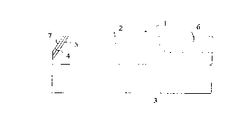
In a bipolar semiconductor-on-insulator transistor device (1) comprising an
emitter region (4), a base region (5), a collector region (2) and a collector
contacting region (6) in a semiconductor wafer, e.g. a monocrystalline silicon
wafer (2), on top of an insulator (3), the base-emitter and collector-base
junctions are tilted relative to the interface between the semiconductor wafer
(2) and the insulator (3). The device can be made by anisotropic etching in
order to produce a tilted surface (7) at an edge of the device or equivalently
a V-groove having tilted sidewalls. The base and emitter regions (5, 4) are
then produced by diffusing suitable donor and acceptor atoms into the material
inside the tilted surface. Such a bipolar semiconductor-on-insulator
transistor combines the high speed features of a lateral semiconductor device
and the high voltage features of a vertical semiconductor device.


French Abstract

Dispositif transistor bipolaire (1) à semi-conducteur sur isolant, comprenant une région d'émission (4), une région base (5), une région collectrice (2) et une région de contact de collecteur (6) sur une plaquette semi-conductrice telle qu'une plaquette de silicium monocristallin (2) sur un isolant (3). Les jonctions base-émetteur et collecteur-base sont inclinées par rapport à l'interface entre la plaquette semi-conductrice (2) et l'isolant (3). Le dispositif peut être réalisé par gravure anisotrope pour obtenir une surface inclinée (7) sur un bord du dispositif ou, de manière équivalente, une rainure en V présentant des parois latérales inclinées. Les régions base et émetteur (5, 4) sont ensuite élaborées par diffusion d'atomes appropriés donneurs et accepteurs dans le matériau contenu à l'intérieur de la surface inclinée. Un tel transistor bipolaire à semi-conducteur sur isolant combine les caractéristiques de vitesse élevée d'un dispositif à semi-conducteur latéral et les caractéristiques de tension élevée d'un dispositif à semi-conducteur vertical.

Claims

Note: Claims are shown in the official language in which they were submitted.

CLAIMS
1. A bipolar semiconductor-on-insulator device (1) comprising an
emitter region (4), a base region (5), and a collector region in
a semiconductor wafer (2) on an insulator (3), characterized in
that the base-emitter and collector-base junctions are tilted in
relation to the interface between the semiconductor wafer (2)
and the insulator (3).
2. A device according to claim 1, characterized in that the
angle of tilt of the base-emitter and collector-base junctions
3 is in the range of 45° ~ 20°.
3. A device according to claim 1 or 2, in the case where the
semiconductor wafer is made of monocrystalline silicon (Si),
characterized in that the angle of tilt of the base-emitter and
collector-base junctions corresponds to the (111) crystal plane
of the silicon wafer (2).
4. A method of producing a bipolar semiconductor-on-insulator
device from a semiconductor wafer (2) on an insulator (3),
characterized by doping the wafer to produce a base region (5)
and an emitter region (4) which are tilted in relation to the
interface between the semiconductor wafer (2) and the insulator
(3).
5. A method according to claim 4, characterized in that the
base-emitter and collector-base junctions are tilted in an angle
in the range of 45° ~ 20°.
6. A method according to claim 4 or 5, in the case where the
semiconductor wafer is made of monocrystalline silicon (Si),
characterized by anisotropically etching the silicon wafer (2)
to expose a (111) crystal plane at one of lateral edges thereof
before doping the base region (5) and the emitter region (4)
parallel to the exposed (111) crystal plane of the silicon wafer
(2).

Description

Note: Descriptions are shown in the official language in which they were submitted.


CA 02243998 1998-07-22
WO 97/33319 - PCT/SE97/00377
B~POLAR SOT DEvrCE ~AV~NG A TILl'ED PN-JUNCrlON. AND A MEIHOD FOR PRODUCTNG
SUCH A DEVICE
TECHNICAL FIE~D
The invention relates to a bipolar semiconductor-on-insulator
5 device as well as to a method of producing such a device.
R~RG~OUND AND PRIOR ART
A large number of bipolar semiconductor devices be designed
without heavily doped, buried layers on semiconductor substrates
has been proposed. There are two basic types of such bipolar
osemiconductor devices, namely lateral devices and vertical
devices.
Lateral devices (see e.g. Stephen A. Parke, Chenming ~u, Ping R.
Ko: "A High-Performance Lateral Bipolar Transistor Fabricated on
Simox", IEEE Electron Dev. Lett., vol. 14, pp. 33-35, Jan. 1993,
~sand R. Dekker, W.T.A. v.d. Einden and H.G.R. Maas: "An Ultra Low
Power ~ateral Bipolar Emitter Technology on SOI", ~993 IEDM
Conference Digest, pp. 7~-77~, are intended for high speed
applications but are able to support only quite small voltages.
Vertical devices (see e.g. Andrej Litwin and Torkel Arnborg:
~"Compact Very High Voltage Compatible Bipolar Silicon-On-
Insulator Transistor", ISPSD'94, Davos, June 1994, and U.S.
Patent No. 4,8~8,624) are intended more for high voltages and
moderate switching velocities.
Isolating shallow lateral devices can be achieved more easily
~than isolating vertical devices since a simple LOCOS or mesa
isolation can be utilized instead of a trench or iunction
isolation. However, the control of base and emitter doping is
difficult, since lateral diffusion has to be utilized. The
lateral devices exhibit lower breakdown voltages BVCeo than
~vertical devices, in which BVCeo = BVC~o. On the other hand,
vertical devices which are capable of supporting high voltages,
suffer from low switching speeds, limited by the transit time
for lateral carrier transport along the semiconductor-insulator
interface below the base due to potential lock-up (see Torkel
~Arnborg: ~Modelling and Simulation of High Speed, High Voltage
Bipolar SOI Transistor with fully Depleted Collector" presented

CA 02243998 1998-07-22
W O 97/33319 - PCT/SE97/00377
in 1994 IEDM Conference Digest).
SUMMARY
The o~ject of the invention is to provide a bipolar semicon-
ductor-on-insulator device which combines the high speed
5 features of a lateral semiconductor device and the high voltage
features of a vertical semiconductor device.
This object is attained by a bipolar semiconductor-on-insulator
device having base-emitter and collector-base junctions which
are tilted.
o~his object is also attAine~ by a method of producing a bipolar
semiconductor-on-insulator device comprising that the base
region and the emitter region are produced to have a tilted con-
figuration.
BRIEF DESCRIPTION OF THE DRAWINGS
t~ The invention will be described in detail by way of a non-
limiting embodiment with reference to the accompanying drawings
in which:
- Fig. 1 is a schematic cross-~ectional view of a bipolar semi-
conductor-on-insulator device,
~- Figs. 2 and 3 are diagrams illustrating calculated dopant
profiles at the emitter of a bipolar device according to Fig. 1,
- Fig. 4 is a diagram illustrating measured dopant pro~iles at
the emitter of a bipolar device according to Fig. 1.
DETATT.F~ DESCRIPTION
~Figure 1 schematically shows an embodiment of a bipolar semi-
conductor-on-insulator device 1, where the semiconductor is a
monocrystalline silicon wafer, the device 1 thus being a
silicon-on-insulator (SOI) semiconductor device. The silicon
wafer ifi denoted 2, whereas the insulator, e.g. a silicon oxide
~layer, is denoted 3 and is located underneath the silicon wafer
as seen in the figure. The device as illustrated has a generally
rectangular cross-section.
The silicon wafer 2 includes an emitter region 4, a base region
5, and a collector contacting region 6, the collector being the
-

CA 02243998 l998-07-22
W 097/33319 - PCT/SE97/00377
region of the bulk silicon material 2 located between the base
region 5 and the collector contacting region 6. In an npn-
transistor the emitter region 4 has an n-doping of e.g. arsenic,
the base region has a p-doping of e.g. boron, the bulk silicon
5 material has a n doping of e.g. arsenic and the collector con-
tacting region 6 has a heavy n-doping of e.g. arsenic. In the
silicon wafer 2, the base-emitter junction and the collector-
base junction are parallel to each other and they are both
tilted in relation to the interface between the silicon wafer 2
~oand the insulator 3. This is accomplished by the fact that the
thin emitter region or layer 4 and the thin base region or layer
5 are tilted in relation to said interface between the silicon
wafer 2 and the insulator 3.
The angle of tilt of the base-emitter and collector-base
15 junctions in relation to the interface between the silicon wafer
2 and the insulator 3, is typically in the range of 45~ + 20~,
i.e. between 25 and 6~~.
The emitter and base regions 4, 5 are located at an upper edge
line of the wafer structure where the structure has a tilted
~surface 7, the configuration being obt~ine~ by cutting away a
corner region of the generally rectangular cross-section. The
emitter and base regions are located at this tilted surface 7,
the emitter region 5 being a thin layer located directly inside
the tilted surface and the base region 4 being a thin layer
~located directly inside the emitter region, the emitter and base
regions thus ext~n~i ng in parallel to the tilted surface 7. The
tilted surface 7 is only a surface of the silicon layer 2 and
does not extend into the insulator layer 3. The collector con-
tacting region 6 is located at the upper edge line of the
~structure which is opposite the edge where the tilted surface 7
is located.
A method of producing the semiconductor device 1 shown comprises
etching anisotropically an SOI film, having a (100) silicon
crystal orientation of the plane along its surface. The etching
~is made with a solution of KOH in order to produce the tilted
surface 7 achieving that this surface will always be located
along a ~111) crystal plane of the silicon wafer 2. The etching

CA 02243998 1998-07-22
W 097133319 - PCT/SE97100377
i8 made only at one of the lateral edges of the SOI film, re-
~uiring that a suitable mask is applied before the etching step.
Thereupon a base region 5 and an emitter region 4 are doped so
that they will ~e parallel to the tilted surface 7 and thus to a
s(lll) crystal plane in the silicon wafer 2, which is supposed to
already include a collector contacting region 6 made in some
earlier processing step. The angle of tilt of the parallel base-
emitter and collector-base junctions will thus correspond to the
angle of tilt of the (111) crystal plane of the silicon wafer 2
10 in relation to its upper surface. Emitter-, base- and collector
con~acts, not shown, are finally produced in some conventional
way such as by ~king heavily doped contacting regions at
suitable places and by producing metallizations on top of these
regions or by making polysilicon structures at suitable con-
15 tacting places.
The method can also be used for producing transistors on a wa~ersuch as for an integrated circuit having several different com-
ponents on the same chip. Then the anisotropic etching is made
to produce V-grooves having sides walls located along (111)
~planes of the silicon monocrystalline material. In the V-
grooves, from the sides thereof suitable dopants are dif~used
into the silicon material to produce the base and emitter
regions. This method will then differ from conventional methods
of producing transistors mainly in the step of producing the V-
~grooves ~efore the diffusion steps or in producing V-grooves
having tilted sidewalls instead of rectangular cross-section
grooves having sidewalls perpendicular to the surface of the
wafer.
The diagram of Fig. 2 shows a one-dimensional simulation of the
~doping profiles as taken perpendicularly to the tilted surface 7
of the emitter 4 for a typical embodiment of a transistor as
described with reference to Fig. 1. The various lines drawn
illustrate the concentrations of arsenic, boron and phosphorous
as functions of the distance from the surface 7. Also, the net
~dopant concentration is shown. In the diagram of Fig. 3 the net
donor concentration and the net acceptor concentrations are
illustrated as functions of the same distance. Also here, the
net dopant concentration is shown.
. . , _

CA 02243998 l998-07-22
-
WO97/33319 - PCT/SE97/00377
In Fig. 4 measured values of the actual concentrations of dopant
atoms are shown for a npn-transistor doped with arsenic and
boron, also as functions of the same perpendicular distance from
v the tilted surface of the emitter region.
sIt is to be understood, however, that other methods in addition
to etching as described above may be used to produce tilted
parallel base-emitter and collector-base junctions. Also,
another crystal surface than the (lll) crystal plane of the
silicon wafer may be exposed for producing the tilted surface to
t~be doped to achieve a base region and an emitter region parallel
to the exposed crystal surface.
The ~ n~ions of the SOI film are chosen in such a way that the
electric field perpendicular to the emitter-base junction will
be reduced. This will increase the breakdown voltage of the
5 semiconductor device. Due to its geometry, the charge is
injected into the collector space charge region in the direction
of the electric field. Since no potential lock-up is present,
and thus, the lateral field is never zero, the transport will be
by drift and not by diffusion 8S in the case of a semiconductor
~device having a fully depleted collector. This feature will make
the semiconductor device as described above faster having a per-
formance comparable to a lateral semiconductor device.
Moreover, it is to be understood that the invention is not re-
stricted to the use of silicon as a semiconducting material in
~the semiconductor-on-insulator device. Instead of silicon, e.g.
GaAs or SiC may equally well be used.

Representative Drawing
A single figure which represents the drawing illustrating the invention.
Administrative Status

2024-08-01:As part of the Next Generation Patents (NGP) transition, the Canadian Patents Database (CPD) now contains a more detailed Event History, which replicates the Event Log of our new back-office solution.

Please note that "Inactive:" events refers to events no longer in use in our new back-office solution.

For a clearer understanding of the status of the application/patent presented on this page, the site Disclaimer , as well as the definitions for Patent , Event History , Maintenance Fee  and Payment History  should be consulted.

Event History

Description Date
Application Not Reinstated by Deadline 2002-03-05
Time Limit for Reversal Expired 2002-03-05
Deemed Abandoned - Failure to Respond to Maintenance Fee Notice 2001-03-05
Inactive: Single transfer 1998-12-08
Inactive: IPC assigned 1998-10-26
Classification Modified 1998-10-26
Inactive: IPC assigned 1998-10-26
Inactive: First IPC assigned 1998-10-26
Inactive: IPC assigned 1998-10-26
Inactive: Courtesy letter - Evidence 1998-10-06
Inactive: Notice - National entry - No RFE 1998-09-28
Application Received - PCT 1998-09-25
Application Published (Open to Public Inspection) 1997-09-12

Abandonment History

Abandonment Date Reason Reinstatement Date
2001-03-05

Maintenance Fee

The last payment was received on 2000-03-03

Note : If the full payment has not been received on or before the date indicated, a further fee may be required which may be one of the following

  • the reinstatement fee;
  • the late payment fee; or
  • additional fee to reverse deemed expiry.

Please refer to the CIPO Patent Fees web page to see all current fee amounts.

Fee History

Fee Type Anniversary Year Due Date Paid Date
Basic national fee - standard 1998-07-22
Registration of a document 1998-12-08
MF (application, 2nd anniv.) - standard 02 1999-03-05 1999-03-01
MF (application, 3rd anniv.) - standard 03 2000-03-06 2000-03-03
Owners on Record

Note: Records showing the ownership history in alphabetical order.

Current Owners on Record
TELEFONAKTIEBOLAGET LM ERICSSON
Past Owners on Record
ANDREJ LITWIN
TORKEL ARNBORG
Past Owners that do not appear in the "Owners on Record" listing will appear in other documentation within the application.
Documents

To view selected files, please enter reCAPTCHA code :


To view images, click a link in the Document Description column. To download the documents, select one or more checkboxes in the first column and then click the "Download Selected in PDF format (Zip Archive)" or the "Download Selected as Single PDF" button.

List of published and non-published patent-specific documents on the CPD .

If you have any difficulty accessing content, you can call the Client Service Centre at 1-866-997-1936 or send them an e-mail at CIPO Client Service Centre.


Document
Description 
Date
(yyyy-mm-dd) 
Number of pages   Size of Image (KB) 
Drawings 1998-07-22 4 56
Claims 1998-07-22 1 44
Abstract 1998-07-22 1 58
Description 1998-07-22 5 263
Cover Page 1998-10-27 1 55
Representative drawing 1998-10-27 1 2
Reminder of maintenance fee due 1998-11-09 1 110
Notice of National Entry 1998-09-28 1 192
Courtesy - Certificate of registration (related document(s)) 1999-02-02 1 115
Courtesy - Abandonment Letter (Maintenance Fee) 2001-04-02 1 182
Reminder - Request for Examination 2001-11-06 1 118
PCT 1998-07-22 7 266
Correspondence 1998-10-06 1 30