Note: Descriptions are shown in the official language in which they were submitted.
- CA 02244016 1998-07-28
P/61277/PS
Detection Circuits
This invention relates to detection circuits and more particularly to circuits used to
detect low level signals in the presence of interfering continuous wave (CW) signals.
Amplitude Shift Key (ASK) or On-Off Key (OOK) modulation is commonly used in
low cost RF systems for use in short range digital control or monitoring systems such as
automotive Remote Keyless Entry, security sensor monitoring and garage door opening. In
OOK modulation, a transmitter is switched on and off to create a data signal comprising
"mark" and "space" periods. The received signal may have varying amplitudes during the
"mark" periods because of variation in distance between the transmitter and receiver. In
ASK modulation, the data signal may be produced by switching a transmitter between high
and low amplitude outputs in which energy is transmitted during "space" periods in addition
to during the "mark" periods. In some forms of ASK modulation, intermediate amplitude
levels may be used to provide a non-binary code. OOK modulation may be considered to be
a form of ASK modulation.
The low cost systems mentioned above are of an unlicensed category and commonly
occupy narrow regions of the RF spectrum, eg. 433.92 + 0.875 MHZ. Since these bands are
not rigorously controlled however it is highly probable that there will be high level
transmissions in the vicinity which can "jam" the wanted signal, interfering to such an extent
that data is not recoverable at a receiver. Such interfering signals may be derived from many
types of sources, for example, from amateur radio transmissions.
CA 02244016 1998-07-28
2 P/61277/PS
Receivers used in these low cost RF systems may be Tuned Radio Frequency (TRF),
super-regenerative discrete designs and superhet integrated circuit designs for example.
Transmissions to be detected are typically irregular and of short duration, say less than one
second.
Suitable receivers often use highly selective RF filters prior to the Low Noise
Amplifier (LNA) and at IF, although their bandwidths must allow for transmission
frequency tolerances in excess of + 100 kHz, with equally slack Voltage Controlled
Oscillator (VCO) tolerances in the receiver for reasons of cost. Data rates are low, normally
0.4 to 5 kBits/s. Consequently, the signal bandwidth into a detector may be in the region of
+ 300 kHz whilst the final data bandwidth is less than 5 kHz. Data filters may be employed
to reduce noise bandwidth and increase sensitivity. However, the detector, being non-
frequency selective, will detect on all signals, wanted and un-wanted, in the wide IF
passband, giving high risk of j~mmin~; occurring.
A number of superhet designs for these applications use Logarithmic IF amplifiers
and a Received Signal Strength Indicator (Log RSSI) as a detector. It is well known that
these circuits are not capable of detecting signals in the presence of CW jammers of similar
RF level. However the benefit of Log RSSI detectors is their instant response time over a
very wide range of signal level, ideal for OOK signals, compared to using a linear IF
amplifier with automatic gain control.
In band continuous interfering IF signals reduce the sensitivity of the RSSI detector
CA 02244016 1998-07-28
3 P/61277/PS
to the wanted signal, as the output is a log function of the input RF level during the 'mark'
and 'space' periods. Also during the 'mark' period such interfering IF signals produce a
signal modulated at the beat frequency (fw-f ), where fw is the wanted IF signal and f is the
j~mming signal. This reduces the mean level of the wanted signal after it is filtered by a data
filter to the extent that, for a j~mming signal at the sarne level or greater than the wanted
signal, the output data signal is zero. Figure 1 shows part of the beat frequency envelope
during the 'mark' period of the wanted signal when the interferer is 6dB higher in power.
Figure 2 is an explanatory diagrarn of the detected signal at the RSSI output of the log
amplifier. Mean signal levels during "mark" and "space" periods are shown with the levels
for "mark" and "space" periods being inverted when compared to the wanted signal without
interferer. The modulation component V is impressed on the wanted signal and when data is
present (not shown in the diagram) the "mark" and "space" amplitudes will vary with it.
The RSSI output is put through a data filter to reduce the noise bandwidth. However
the CW j~mming signal produces a beat frequency such that there is no longer a low
frequency data component present, as shown in Figure 3.
Typically systems using Log RSSI detectors are only capable of detecting wanted
signals with signal level ratios of:
jam ~5--3dB
wanted
According to the invention there is provided a detection circuit for a modulated
CA 02244016 1998-07-28
4 P/61277/PS
signal having mark and space intervals comprising dc restoration means for dc restoring a
received modulated signal on signal peaks corresponding to mark intervals. The signal
applied to the dc restoration means may undergo some processing prior to being applied to
the dc restoration means. The received modulated signal is ac coupled to the dc restoration
means.
This invention considerably reduces the effect of beat frequencies due to j~mming
signals in the IF, enabling the wanted signal to be detected in the presence of a j~mminp~
signal level ratio of:
jam ~ +20dB
wanted
By using the invention, it is possible to recover a low level wanted ASK signal from
CW interferer which would otherwise prevent the wanted signal from being recovered. An
antijam ASK detection circuit in accordance with the invention may enable ASK and OOK
signals to be detected in the presence of +20dB CW j~mming signals relative to the wanted
"mark" level. This gives an overall improvement of +23dB over the RSSI detector alone.
The detection circuit may also be used as the detector directly on the signal output of
a linearly automatic gain controlled IF amplifier where greater performance improvement
may be realised.
According to a first feature of the invention, a receiver includes a detection circuit in
CA 02244016 1998-07-28
P/61277/PS
accordance with the invention.
According to a second feature of the invention, a system includes a transmitter for
transmitting a modulated signal having mark and space intervals and a receiver incorporating
a detection circuit in accordance with the invention.
One way in which the invention may be performed is now described by way of
example with the reference to the accompanying drawings in which:
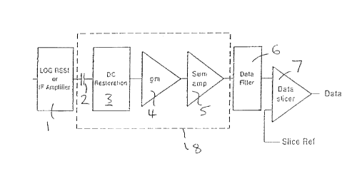
Figure 4 is a schematic block diagram of a detector circuit in accordance with the
invention;
Figures 5(a), 5(b), 6(a), 6(b), 7, 8(a) and 8(b) are explanatory diagrarns relating to
the operation of the circuit shown in Figure 4; and
Figure 9 is a circuit realisation of part of the arrangement shown in Figure 4.
With reference to Figure 4, a detector circuit in accordance with the invention
comprises a log RSSI detector 1. An ASK modulated signal is received at the input of the
amplifier. In the absence of a j~mming signal, the input to the log amplifier takes the form
shown in Figure 5(a). When j~mming is present however, the signal is corrupted and may
appear as shown in Figure 5(b). Figures 6(a) and 6(b) show the wave forms at the output of
the log amp RSSI detector I in the absence and presence respectively of a j~mming signal.
- CA 02244016 1998-07-28
6 P/61277/PS
As can be seen, the j~mming signal has a considerable effect on the output signal. The
output of log RSSI 1 is applied to a coupling and dc restoration capacitor 2 and to dc
restoration circuit 3. The ac coupled signal at capacitor 2 is dc restored on the signal peaks
defined by the higher RF level corresponding to the "mark". The lower signal which
corresponds to the "space" is not used for dc restoration because of its very much lower
signal to noise ratio. Following dc restoration, the signal is applied to a transconductance
amplifier 4 which amplifiers the peak of the signal non-linearly, such that the output
current, Is is
I =I . .exp--(V. -Y ).N
s blas KT In clamp
where IbiaS is the nominal dc current in the transistor with no input signal, and
(Vin - Vclamp) is the dc restored input signal relative to the clamp level. N is a multiplying
factor which is dependent on the amplitude and the mark/space ratio of the wanted signal,. e
is the electron charge, k is Boltzmann's constant and T is temperature in Kelvin.
The current Is from the transconductance amplifier 4 is summed at 5 with an
amplifier standby current to give an output which corresponds to the amplified peaks of the
signal during the "mark" period of the wanted signal. This gives an output signal V out,
where VOut = -R.(Is - Ibjas). The resulting output signal is then applied to a data filter 6 and
data slicer 7 to provide a data output signal. The capacitor 2, dc restoration circuit 3,
transconductance amplifier 4 and sllmming amplifier 5 may be considered to form an anti-
jam detection circuit 8, as indicated by a broken line in Figure 4.
CA 02244016 1998-07-28
7 P/61277/PS
As the output signal from the sllmming amplifier 5 has a relatively large differential
between the mean levels during the "mark" and "space" intervals of the wanted signal, the
data slicer 7 is capable of slicing the signal even in the presence of CW interferers of greater
than 20dB higher. Figure 7 illustrates the relative difference between the mean output levels
of the "mark" interval and the "space" interval together with the signal V at the output of the
sllmming amplifier 5 in the absence of data. Figures 8(a) and 8(b) show the output of the
anti jam circuit 8 with and without respectively a jamming signal.
Figure 9 is a circuit realisation of the arrangement shown in Figure 4. In this circuit,
a PNP Ql serves a dual function as the dc restoration circuit, discharging the coupling
capacitor C during signal peaks, and also as a non-linear high gain amplifier. The coupling
capacitor C, as in many dc restoration circuits, stores the charge for the dc restoration
voltage.
As described above, the signal applied to the antijam circuit is derived from a log
RSSI 1. In other implementations, the signal applied to the antijam circuit may be taken
from the output of an IF amplifier.